Abstract
Precise patterning of metals is required for diverse microfluidic and microelectromechanical system (MEMS) applications ranging from the separation of proteins to the manipulation of single cells and drops of water-in-oil emulsions. Here we present a very simple, inexpensive method for fabricating micropatterned electrodes. We deposit a thin metal layer of controlled thickness using wet chemistry, thus eliminating the need for expensive equipment typically required for metal deposition. We demonstrate that the resulting deposited metal can be used to fabricate functional electrodes: The wet-deposited metal film can sustain patterning by photolithography down to micron-sized features required for MEMS and microfluidic applications, and its properties are suitable for operative electrodes used in a wide range of microfluidic applications for biological studies.
INTRODUCTION
Creating a fully integrated laboratory on a chip would enable complete processing and analysis of nanoliter- to picoliter-scale sample volumes in a single experiment. To achieve this goal requires integrating a range of functions into one device, such as the ability to sort and lyse single cells,1 electrofuse cells,2 electroform lipid vesicles and measure ion channel currents,3 as well as manipulate and coalesce drops of water-in-oil emulsions.4 Many of these applications require an electric field and current to be generated on chip, which necessitates that electrodes are integrated into the device.
A simple, inexpensive way to fabricate microelectrodes is by injection molding: Molten solder is injected into microfluidic channels and hardens upon cooling, conforming to the form of the fluidic channel.5 With microfluidic channels providing a mold for the metal, micron-scale features can be achieved and no additional alignment steps are required. However, this method produces electrodes that are separated from flow channels by a polydimethylsiloxane (PDMS) wall; this configuration is suitable for dielectrophoresis that requires only a field gradient, but direct current applications are not possible since the electrodes are not in contact with the aqueous phase. To achieve electrodes that can contact the aqueous phase and can also be used for nonmicrofluidic applications, the PDMS templating channels are temporarily placed on the substrate and peeled away subsequent to metal deposition, leaving the electrode-patterned substrate.6 However, this method requires the additional step of fluidic channel fabrication and is best for patterning continuous features conforming to the flow channel with heights greater than microns. Metallic features can also be patterned using microcontact printing where electroless silver is the substrate;7, 8, 9 however, the resolution of the printed pattern may be limited by lateral diffusion of applied ink and deformation of the elastomeric stamp. Deposition of metals onto a substrate can additionally be achieved by electroplating, sputter deposition, or vapor deposition; electrodes are subsequently patterned using photolithography;10 yet these methods are expensive and require equipment that is typically housed in dedicated facilities. To circumvent the cost and need for specialized equipment for metal deposition, we suggest a way to deposit metals for micropatterning that matches the simplicity and ease of soft lithography.
Here we describe a simple, inexpensive, and accessible method to generate patterned electrodes on a glass substrate with micron-scale feature sizes. We use the century-old chemistry of Tollens’ reaction to deposit a silver film of the desired thickness on glass. We show that the metal can be patterned using standard photolithography techniques to form features suitable for application in microelectromechanical systems (MEMS) or microfluidic applications. The resulting silver electrodes can be coated with a thin layer of PDMS or silane solution for incorporation into PDMS microfluidic devices.
MATERIALS AND METHODS
Deposition of metallic silver on glass slide
All experiments are performed at room temperature unless otherwise indicated. Concentrated ammonium hydroxide is added dropwise to 10 ml 0.1M silver nitrate solution until the initial precipitate dissolved. We then immediately add 5 ml 0.8M KOH solution to form a dark precipitate, followed by just enough additional ammonium hydroxide to redissolve the precipitate. The resulting colorless solution is used immediately in the following steps, and any excess is destroyed by acidification with hydrochloric acid. (Caution: Explosive silver nitride may form if the solution is allowed to stand for a prolonged time.)
A glass slide is cleaned thoroughly with ethanol and air dried. The silver solution is placed drop by drop onto the slide to form a puddle that covers the entire surface (21 drops are required to cover a 75×38 mm2 slide). To reduce the soluble silver ammonia complex, 0.5M glucose solution amounting to one-third the volume of the puddle is added dropwise. The slide is gently agitated for 1 min to mix the overlying puddle and allowed to stand for 2 min. The deposition solution is poured off and the slide is washed thoroughly with de-ionized water. If necessary, additional deposition cycles are performed on the wet slide to produce a thicker coating. Typically at least two deposition cycles are required to form an even coating. The slide is air dried upon completion of deposition. The resulting silver coating is gently polished using a nitrile-gloved fingertip, cleaned with de-ionized water and ethanol, and air dried.
Measurement of silver film thickness
To measure the height of the silver features, we use a stylus profilometer (KLA Tencor, Milpitas, CA) with a scan speed of 100 μm∕s and a sampling rate of 200 Hz.
Micropatterning by lithography and etching
We use standard lithographic techniques to micropattern the silver film. In brief, the silver-coated glass substrate is dehydrated on a hotplate at 110 °C for 15 min and cooled. The substrate is spincoated with Shipley 1813 positive photoresist (Shipley Co. LLC, Marlborough, MA) at a final speed of 4000 rpm for 60 s and immediately soft baked at 95 °C for 1 min. A positive Mylar photomask is placed on the substrate and exposed to UV with an intensity of 150 mW∕cm2 (OAI, San Jose, CA). The exposed substrate is developed in a sodium hydroxide-based developer for 1 min while swirling and rinsed with de-ionized water. Unprotected silver coating is etched away by sonicating the wet substrate for 1.5–2 min in a 30:1:1 v∕v/v mixture of de-ionized water, 30% hydrogen peroxide, and concentrated ammonium hydroxide. The etchants are rinsed away with de-ionized water, and the protective photoresist layer is removed with acetone to reveal the patterned silver coating. We compare the properties of our deposited silver electrodes with commercially available indium tin oxide (ITO) (Delta Technologies, Ltd., Stillwater, MN). ITO electrodes are patterned following the same procedure but with an exposure of 100 mW∕cm2 and etching with a concentrated hydrochloric acid for 20 min.
RESULTS AND DISCUSSION
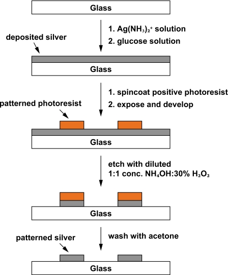
We present a very simple method to deposit functional silver on a surface and to pattern the film to form micron-sized metal features. A schematic of the procedure is shown in Fig. 1. First, a thin silver film is deposited by Tollens’ reaction. Also known as the silver mirror reaction, Tollens’ reaction is used widely in carbohydrate chemistry for detecting reducing sugars. In the presence of a reducing sugar, such as glucose, aqueous ionic silver in the form of diamine silver complex is reduced to metallic silver, which forms a silver mirror in a clean glass vessel. Our work shows that this chemistry is capable of producing a silver film of uniform thickness that is a very good substrate for micropatterning by photolithography. To obtain even coverage and thickness of the metallic film, we ensure that the precipitation proceeds gradually by adding the glucose solution dropwise and thoroughly mixing the deposition solution immediately after adding the glucose solution. This deposition method is simple to perform in any laboratory with access to a fumehood. Moreover, all reagents used are much safer and environmentally benign in comparison to those used in depositing and etching other metals. Furthermore, the entire process requires only minutes to complete.
Figure 1.
Schematic diagram of micropatterning electrodes. Freshly prepared Ag(NH3)2+ solution is dropped uniformly over a glass substrate until the surface is entirely covered. Glucose solution is dropped uniformly over the substrate, and the substrate is gently agitated to allow even mixing of the solutions. Deposition is complete within 3 min. After agitation for 5 min, the deposition solution is rinsed off with water. Deposition is repeated once again to achieve an even coating. The substrate is dehydrated on a hotplate, and standard photolithography methods are used to pattern positive photoresist over the silver coating. The unprotected silver is etched away by sonicating in a diluted 1:1 (v/v) NH4OH:30% H2O2. Finally, the remaining photoresist is dissolved away with acetone to reveal the patterned silver.
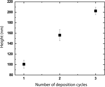
The thickness of the silver film is controlled by the number of deposition cycles. Using a profilometer, we measure the silver film thickness for one, two, and three depositions. The thickness is proportional to the number of deposition cycles, as shown in Fig. 2. These results demonstrate how the electrode height can be easily controlled by the number of depositions.
Figure 2.
Thickness of silver film depends on number of layers deposited. We control the electrode height by varying the number of layers deposited. The height of a polished, deposited silver film is measured by profilometry. Error bars represent standard deviation of at least three independent measurements.
To compare the functionality of our silver-coated device with a commercially available coated substrate, we use glass slides coated with ITO. We measure the surface resistance of deposited silver films to be less than 0.1–0.01 that of a ITO-coated piece of glass rated at 30–60 Ω∕sq, which roughly correlates to 30–60 nm (Table 1). We find that surface resistance decreases with increasing film thickness.
Table 1.
Surface electrical resistance. Resistance is measured with multimeter electrodes spaced 1 cm apart. ITO rated at 30–60 Ω∕sq is rated at 48.3±2.6. Reported values are the average of at least ten measurements with standard deviation.
| One deposition | Two depositions | Three depositions | |
|---|---|---|---|
| Average resistance | 1.2±0.2 | 0.6±0.1 | 0.4±0.1 |
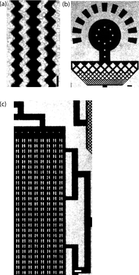
We generate patterned electrodes by spincoating positive photoresist onto the metal-coated substrate. Photolithography is routinely used to generate micropatterned substrates; here we describe a procedure to micropattern wet-deposited silver layers. A mask with the desired template is placed on the substrate and is exposed to UV light. The metal is subsequently etched from the surface at room temperature using a noncorrosive, silver-specific etchant composed of ammonium hydroxide and hydrogen peroxide: The electrode pattern remains where the metal does not come into contact with the etchant [Fig. 3a]. Etching occurs instantaneously with vigorous effervescence upon contact with a concentrated etchant. While the use of a concentrated etchant is suitable for patterning large features, the rapid etching rate can erode micron-sized features and the effervescence may interfere with contact between the etchant and the substrate, leading to inhomogeneous etching and lift-off of the photoresist. To achieve even etching and higher resolution of the patterned electrodes, we carry out the etching step in a sonication bath with a diluted etchant. Using this technique, we fabricate electrodes ranging in size from microns to hundreds of microns, as shown in Fig. 3. The spatial resolution of the electrodes is limited by the photolithography process. These results confirm that a metal film deposited by wet chemistry can sustain micron-scale feature sizes patterned by photolithography. Moreover, these silver films can be deposited on substrates of varying surface area: Uniform deposition over areas much greater than achieved in this work may be facilitated by spray-based electroless silvering.11 Thus, electrodes of varying heights and geometries can be rapidly fabricated in this simple, inexpensive way.
Figure 3.
Wet-deposited silver films sustain micropatterning of micron-scale features. By patterning with photoresist and subsequently etching, electrodes with the desired geometry are fabricated as shown in these images. Note the micron-scale features that can be achieved. (a) Micropatterning after one deposition cycle; [(b) and (c)] micropatterning after three deposition cycles. Scale: 10 μm.
Electrodes patterned on glass are indispensable for many MEMS applications and can also be easily incorporated into PDMS microfluidic devices: By spincoating a thin layer of PDMS onto the electrodes, the silver-coated substrate can be bonded to a PDMS slab with fluidic channels by plasma treatment or partial curing.12 Alternatively, electrodes can be treated with a silane solution for bonding to PDMS. While silver is relatively inexpensive and inert, other metals such as gold, copper, or platinum13 can also be deposited using wet chemistry, albeit with the use of more toxic and corrosive agents. To further reduce costs, resistant tape could be used for micropatterning, and an inexpensive UV light source can also be used; however, the resolution of features patterned using noncollimated UV light may be compromised. Glass coated with conductive materials, such as ITO, is commercially available and can also be micropatterned.14 However, compared to our deposited silver electrodes, ITO is more expensive and less conductive. Moreover, control over the thickness of the deposited silver film gives the user the ability to control electrode geometry, making it possible to inexpensively fabricate micron-sized silver wires as well as isolated features.
CONCLUSIONS
We demonstrate that depositing a silver film using wet chemistry is a suitable substrate for micropatterning electrodes with micron-sized features using photolithography. This method is simple and inexpensive and thus offers major advantages over existing techniques in cost, ease, and speed of fabrication.
ACKNOWLEDGMENTS
We acknowledge use of equipment in the Center for Nanoscale Systems (CNS), Harvard University. A.C.R. is a Human Frontiers Science Program Cross-Disciplinary Fellow. This work is also supported by Human Frontiers Grant No. RGP0004∕2005-C102, NSF Contract Nos. DMR-0602684 and DBI-649865, and Harvard MRSEC Contract No. DMR-0213805.
References
- Fiedler S., Shirley S. G., Schnelle T., and Fuhr G., Anal. Chem. 70, 1909 (1998). 10.1021/ac971063b [DOI] [PubMed] [Google Scholar]
- Skelley A. M., Kirak O., Suh H., Jaenisch R., and Voldman J., Nat. Methods 6, 147 (2009). 10.1038/nmeth.1290 [DOI] [PMC free article] [PubMed] [Google Scholar]
- Zagnoni M., Sandison M. E., and Morgan H., Biosens. Bioelectron. 24, 1235 (2008). 10.1016/j.bios.2008.07.022 [DOI] [PubMed] [Google Scholar]
- Ahn K., Agresti J., Chong H., Marquez M., and Weitz D. A., Appl. Phys. Lett. 88, 264105 (2006). 10.1063/1.2218058 [DOI] [Google Scholar]
- Siegel A. C., Shevkoplyas S. S., Weibel D. B., Bruzewicz D. A., Martinez A. W., and Whitesides G. M., Angew. Chem., Int. Ed. Engl. 45, 6877 (2006). 10.1002/anie.200602273 [DOI] [PubMed] [Google Scholar]
- Hong C., Bao D., Thomas M. S., Clift J. M., and Vullev V. I., Langmuir 24, 8439 (2008). 10.1021/la801752k [DOI] [PubMed] [Google Scholar]
- Hsu C. H., Yeh M. C., Lo K. L., and Chen L. J., Langmuir 23, 12111 (2007). 10.1021/la7023988 [DOI] [PubMed] [Google Scholar]
- Xia Y., Venkateswaran N., Qin D., Tien J., and Whitesides G. M., Langmuir 14, 363 (1998). 10.1021/la9707080 [DOI] [Google Scholar]
- Tate J., Rogers J. A., Jones C. D. W., Vyjas B., Murphy D. W., Li W., Bao Z., Slusher R. E., Dodabalapur A., and Katz H. E., Langmuir 16, 6054 (2000). 10.1021/la991646b [DOI] [Google Scholar]
- Wang L., Flanagan L., and Lee A. P., J. Microelectromech. Syst. 16, 454 (2007). 10.1109/JMEMS.2006.889530 [DOI] [Google Scholar]
- Durney L. J., Electroplating Engineering Handbook (Van Nostrand Reinhold, New York, 1984). [Google Scholar]
- Eddings M. A., Johnson M. A., and Gale B. K., J. Micromech. Microeng. 18, 067001 (2008). 10.1088/0960-1317/18/6/067001 [DOI] [Google Scholar]
- Simpson R. and Berberian J. G., Rev. Sci. Instrum. 47, 198 (1976). 10.1063/1.1134579 [DOI] [Google Scholar]
- Kim H. and Kwak J., J. Electroanal. Chem. 577, 243 (2005). 10.1016/j.jelechem.2004.11.035 [DOI] [Google Scholar]


