Abstract
Printed spiral coils (PSC) are viable candidates for near field wireless power transmission to the next generation of high performance neuroprosthetic devices with extreme size constraints, which will target intra-ocular and intracranial spaces. Optimizing the PSC geometries to maximize the power transfer efficiency of the wireless link is imperative to reduce the size of the external energy source, heating of the tissue, and interference with other devices. Implantable devices need to be hermetically sealed in biocompatible materials and placed in a conductive environment with high permittivity (tissue), which can affect the PSC characteristics. We have constructed a detailed model that includes the effects of the surrounding environment on the PSC parasitic components and eventually on the power transfer efficiency. We have combined this model with an iterative design method that starts with a set of realistic design constraints and ends with the optimal PSC geometries. We applied our design methodology to optimize the wireless link of a 1 cm2 implantable device example, operating at 13.56 MHz. Measurement results showed that optimized PSC pairs, coated with 0.3 mm of silicone, achieved 72.2%, 51.8%, and 30.8% efficiencies at a face to face relative distance of 10 mm, in air, saline, and muscle, respectively. The PSC which was optimized for air could only bear 40.8% and 21.8% efficiencies in saline and muscle, respectively, showing that including the PSC tissue environment in the design process can result in more than 9% improvement in the power transfer efficiency.
Index Terms: Printed spiral coils, inductive wireless links, implantable microelectronic devices, neuroprostheses, power transmission efficiency, telemetry
I. Introduction
Cochlear implants, spinal cord stimulators, infusion pumps, and artificial hearts are among an ever-growing number of implantable devices that are wirelessly powered across the skin barrier through a pair of inductively coupled coils [1]. A common requirement among these otherwise diverse biomedical devices is that their average power consumption is higher than what a battery, fitting within the anatomically available space for implantation, can provide.
Research is currently underway to develop a whole new group of implantable devices such as retinal implants and intracranial brain-computer interfaces (BCI) with even stricter size constraints. These are expected to be placed inside the eyeball through a 5 mm incision or within the 1 ~ 3 mm epidural spacing between the outer surface of the brain and the skull [2], [3]. Therefore, the need for more efficient wireless power transmission from outside into the human body, with much smaller footprint, is only expected to grow.
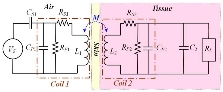
Fig. 1 shows a simplified schematic diagram of a transcutaneous inductive power transmission link, which operates like a transformer. L1 is the primary coil that is attached to the skin from outside of the body, driven by an AC source, VS, which is often an efficient class-E power amplifier [4]. L2 is the secondary coil that is implanted under the skin flap along with the rest of the implant electronics. A pair of permanent magnets, one in the center of each coil can align and hold them together to maximize their mutual inductance, M. Coil windings have parasitic resistance and capacitance associated with them, which are represented in Fig. 1 by lumped elements RS, RP, and CP. Capacitors CS1 and C2 are also added to form a pair of resonant LC-tank circuits with L1 and L2, respectively, at the power carrier frequency, f.
Fig. 1.
Simplified schematic diagram of the inductive link with lumped equivalent circuit components.
So far these coils have been fabricated with thin wires using sophisticated winding machinery [5]. However, the need for much smaller footprints in the next generation of high performance implantable devices calls for higher geometrical precision and potential for integration on chip or on package. This would require microfabrication techniques that result in lithographically defined planar structures that are known as printed spiral coils (PSC). PSCs offer more flexibility in defining their characteristics, and have the ability to conform to the body curvature if fabricated on thin flexible substrates such as polyimide or parylene [6]. Rigid hermetically sealed PSCs can also be fabricated on silicon chips or low temperature co-fired ceramic (LTCC) packages using micromachining (MEMS) technology [7]–[9].
Design and optimization of inductive links with coils made of 1-D filaments have been well studied over the last few decades to find the coil geometries and circuit elements in Fig. 1 that would maximize the amount of power induced in L2 [5], [10]-[15]. We recently summarized these studies in [16] and combined the theoretical foundation of optimal power transmission in inductive links with simple models that would indicate M between a pair of PSCs, their quality factors, and parasitic components. The result was an iterative PSC design methodology that starts with a set of realistic design constraints imposed by the application and PSC fabrication process, and ends with the optimal PSC geometries for maximum power efficiency [16].
For the sake of simplicity, our models in [16] did not include the effects of PSC surrounding environment. In other words, we only considered the PSC operation in air, which is appropriate for radio frequency identification (RFID) [17]. However, implantable devices are hermetically sealed in biocompatible materials and surrounded by the conductive tissue underneath the skin. Considering the effects of surroundings in PSC models is imperative in the optimization process because it can affect the PSC parasitic components in Fig. 1, which in turn affect the power transfer efficiency.
In this paper, we improve the accuracy of our models in section II by adding the effects of the PSC coating, substrate, and surrounding environments. We also consider some of the key secondary effects in estimating parasitic components, which play an important role in indicating the PSC quality factor, Q. In section III, we utilize the new models in the same iterative optimization method as in [16], using a combination of closed form equations in MATLAB (MathWorks, Natik, MA) and verification in finite element analysis (FEA) tools in HFSS (Ansoft, Pittsburgh, PA). The result is three sets of PSCs, which geometries are optimized for air, saline, and muscle environments. These PSCs were fabricated on FR4 and characterized in all three environments in section IV to compare their power transfer efficiency, and validate our PSC models and iterative design procedure.
II. Theoretical Modeling of Implanted PSCs
The lumped equivalent circuit model of each PSC in Fig. 1 is enclosed in dash-dot boxes. In the following, we construct a realistic theoretical model for PSCs and discard the numerical subscript wherever we refer to both implanted and external PSCs. The lumped parasitic components of the PSC model are influenced by its geometry, material composition, and surrounding environment.
A. Inductance
In this work, all PSCs are square shaped with rounded corners that have a radius of about a tenth of the side length of the PSC (do/10) to eliminate sharp edges. Several closed-form equations have been proposed to approximate L in PSCs. We adopted (1) from [18] for square shaped coils,
| (1) |
where n is the number of turns, μ = μ0μr is permeability, and davg = (do + di)/2, where do and di are the outer and inner side lengths of the coil, respectively. ϕ = (do − di)/(do + di) is a parameter known as fill factor, which changes from zero, when all the turns are concentrated on the perimeter in filament coils, to one, when the turns spiral all the way to the center of the PSC. The accuracy of (1) has an indirect relationship with the s/w ratio, where w and s are the PSC metal line width and spacing, respectively. According to [18], the error in (1) is 8% for s/w = 3 and increases for s/w > 3. Moreover, the accuracy of (1) degrades with ϕ ≤ 0.1 or n ≤ 2.
B. Capacitance
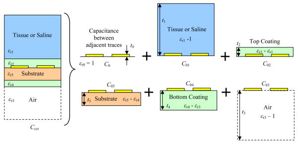
Parasitic capacitance, CP, is mainly determined by the spacing between planar conductive traces and their surrounding materials. Implantable PSCs are implemented on organic, ceramic, or silicon substrates and coated by an insulator such as Parylene or silicone. When implanted, they are surrounded by tissue and fluids that have high permittivity, which significantly increase the parasitic capacitance of the PSCs compared to when they are operated in air. To model the unit length parasitic capacitance of an implanted PSC, we can consider it as a coplanar stripline sandwiched between several layers of dielectric substrates, as shown in Fig. 2.
Fig. 2.
Modeling of the parasitic capacitance created by the multilayer material surrounding the external PSC [19].
In order to calculate the capacitive coupling between coplanar conductors embedded in a multilayer structure, the effective relative dielectric constant, εr-eff, of the multilayer structure has to be estimated. It should take into account the effect of all layers and their thicknesses as opposed to only one surrounding material. Conformal mapping is one of the spatial transformation schemes mainly used in calculation of static two-dimensional unbounded field problems. Using conformal mapping and superposition of partial capacitances, we have derived the following analytical equations [19]–[21].
Fig. 2 shows the cross section of two traces of the external PSC. The planar metal traces are implemented on a substrate that provides mechanical support and coated on both sides by an insulator. One side of the PSC is air and the other side is the tissue or saline (in some of our measurements). To simplify our analysis, we have considered the tissue only as a single homogeneous layer. To be more realistic, one should discriminate between the skin, fat, muscle, blood, and bone properties [26], [27]. From conformal mapping technique and superposition of individual layers, the total capacitance per unit length of the external PSC can be expressed as
| (2) |
where C0 is the capacitance between adjacent traces in free space and C0i (i = 1 ~ 5) is the additional partial capacitance of each planar dielectric layer in Fig. 2. Theoretically,
| (3) |
where K(k0) is the complete elliptic integral of the first kind [19]. εr-eff of coplanar PSC traces embedded in Fig. 2 multilayer structure can be found from,
| (4) |
where εri and ti are the relative dielectric constant and thickness of dielectric layers in Fig. 2, respectively [19]–[21].
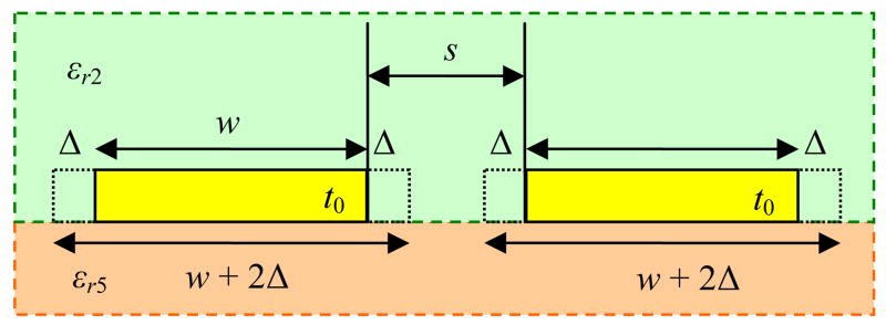
Up until this point, we have not yet considered the effect of the PCS metal thickness, t0, which increases all components of Cext in (2). A good way to include t0, according to [21], is to adjust the PSC line width and spacing by 2Δ, where
| (5) |
and εe is the mean value of the permittivities of the layers in contact with the strips, as shown in Fig. 3.
Fig. 3.
Modification of the PSC line width and spacing to account for the metal thickness, t0 [21].
In order to access the PSC inner terminal, a conductor should bridge across all other turns of the PSC in a different layer and make a connection to the PSC metal layer through a via. This would result in additional parasitic capacitance between the two overlapping metal layers. The overlapping trace can be considered a microstrip line with the overlapping trace capacitance of
| (6) |
where Aov is the overlapping area and tov is the spacing between the two metal layers, which could be equal to t5 in Fig. 2 if the substrate has only two metal layers, one on each side. According to [33], the effective dielectric constant between two conductive plates can be found from,
| (7) |
which includes the fringing effect and thickness of the conductive traces. In our case, since t5 is relatively large, Cov is less than 2 % of the total parasitic capacitance. However, Cov can be significant in integrated or micromachined (MEMS) PSCs, where multiple metal layers are separated by thin dielectric films. Overall, the total parasitic capacitance of the external PSC can be calculated from,
| (8) |
where lc is the PSC conductor length, found from [16],
| (9) |
For the implanted PSC, we can utilize (2) ~ (9) with the exception that the dielectric layer 3 (air) should be replaced by the tissue properties, similar to layer 1, depending on the anatomical location of the implanted device.
C. Series Resistance
The series resistance, RS, is dominated by the DC resistance of the PSC conductive trace,
| (10) |
where ρc is the resistivity of the PSC conductive material, which is often a metal with low resistivity such as gold, platinum, or copper. The skin effect increases the AC resistance of the PSC at high frequencies
| (11) |
| (12) |
where δ is the skin depth, μ0 is the permeability of space, and μr is the relative permeability of the metal layer [22].
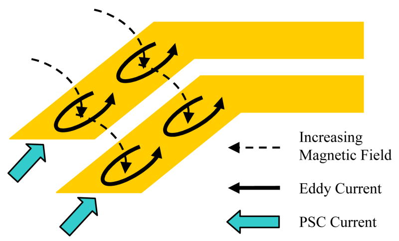
Another effect that contributes to the PSC parasitic resistance is the current crowding caused by the eddy currents, illustrated in Fig. 4. When the magnetic fields of the external PSC or adjacent turns in the same PSC penetrate a planar trace normal to its surface, eddy currents are generated within that trace in a direction that opposes the changes in the magnetic field according to Lenz’s law. For example, in Fig. 4, the direction of the eddy currents corresponds to an increasing magnetic field. These currents add to the current passing through the inner side of the PSC trace, nearest to the center of the spiral, and subtract from the current passing through the outer side. This constriction in the current increases the effective resistance compared to a uniform flow throughout the trace width. The modified resistance by including the effect of eddy currents can be expressed as,
Fig. 4.
Demonstration of the current crowding effect [23].
| (13) |
| (14) |
where ωcrit is the frequency at which the current crowding begins to become significant and Rsheet is the metal trace sheet resistance [23]. Therefore, RS at the power carrier frequency can be defined as RDC when it is modified by the skin and eddy current effects [24].
| (15) |
D. Parallel Resistance
At low RF frequencies, the parallel resistance, RP, in the PSC model of Fig. 1 is resulted mainly from the dielectric loss and can reduce the PSC quality factor. Most dielectric materials used in the PSC substrate and coating have small dielectric loss, resulting in very large RP. In comparison, the tissue is significantly more conductive and its effect should be considered in a multilayer material environment.
We use the partial conductance technique combined with the conformal mapping. Dielectric losses can be described by the loss tangent of each material, tan(δ), which is related to its conductivity, σ = ε0εrωtan(δ). The conformal transformations required for the evaluation of partial conductivities due to different layers are similar to the partial capacitances described in section II. B [21]. For the external coil, shown in Fig. 2, the equivalent conductance of the PSC unit length is going to be
| (16) |
where tan(δ3) = 0 for air. The same equation can be used for the internal coil equivalent conductance.
E. PSC Quality Factor
From (1)–(16), we can derive all the parameters needed for calculating the overall impedance and Q of the implanted and external PSCs,
| (17) |
| (18) |
From these equations, we can infer that the higher parasitic capacitance resulted from implantation decreases the PSC quality factor, and consequently the power efficiency.
F. Mutual Inductance and Power Transfer Efficiency
A PSC can be considered a set of concentric single-turn loops with shrinking diameters, all connected in series. Therefore, once we find the mutual inductance between a pair of parallel single-turn loops at a certain coupling distance, d, the mutual inductance of a pair of PSCs, M, can be found by summing the partial values between every turn on one PSC and all the turns on the other PSC [12], [16], [25]. Using M, we can find the PSCs’ coupling coefficient, which is the key parameter in power transfer efficiency,
| (19) |
It can be shown mathematically that the highest voltage gain and efficiency across an inductive link can be achieved when both LC-tanks are tuned at the power carrier frequency,
| (20) |
In practice, the secondary PSC is often loaded by the implant electronics, RL, as shown in Fig. 1. The loaded secondary quality factor at resonance can be found from [17],
| (21) |
The inductive link power transfer efficiency can then be calculated from PSCs’ k and quality factors [16],
| (22) |
It should be noted that most aforementioned parameters in PSCs are interrelated. For example, increasing n in PSCs without changing do can increase their L and k. However, it may also decrease Q by increasing RS due to increased l and reduced w. Therefore, there are optimal PSC geometries that would maximize η12 as we have previously showed in [16]. Another important parameter is the VS output resistance, not shown Fig. 1, which is out of the scope of this paper and needs be considered along with the driver’s efficiency [4].
III. Optimization of Printed Spiral Coils
A. Optimal Coil
In this section, we use the detailed models built in section II to design three sets of coils optimized for air, saline, and muscle tissue environments. The material properties of these volume conductors are summarized in Table I [26], [27]. We have adopted the iterative design procedure, described in [16], which starts with a set of design constraints and initial conditions imposed by the PSC application and fabrication process, and ends with the optimal geometries of the PSC pair that maximizes η12.
Table I.
Material Properties*
| Material | Air | Saline | Muscle | FR4 | Silicone |
|---|---|---|---|---|---|
| f [MHz] | 13.56 | 13.56 | 13.56 | 13.56 | 13.56 |
| σ [S/m] | 0 | 0.60 | 0.58 | 1.33e-4 | 2.26e-6 |
| εr | 1 | 78 | 136 | 4.4 | 3.0 |
| tan(δ) | 0 | 10.2 | 6.0 | 0.04 | 0.001 |
We have designated the size of the implant to be 10×10 mm2, which is reasonable for a retinal or cortical visual prosthesis [2], [6]. The nominal coupling distance between the PSCs is considered d = 10 mm and the power carrier is set at 13.56 MHz to comply with RFID standards [17]. However, it could be set to any other band in 0.1~50 MHz range, as long as it is well below the PSCs’ self resonance frequency (SRF) [28]. We have also used HFSS simulations to verify and fine tune the values suggested by the theoretical model, when they were out of the valid range of our equations (ex. PSC31).
Table II shows the geometries of the resulting PSCs, specifically optimized for each environment along with the simulation results for Q, k, and η12, when the PSC pair is perfectly aligned. It should be noted that k is the highest in Set-1, resulting in maximum efficiency in the air. However, Q of Set-1 and Set-2 are both smaller than Q of Set-3 in the muscle environment, which results in Set-3 showing the highest efficiency in muscle. Further, it can be seen that for the same implant size and coupling distance, the outer diameter (side length) of the external PSC, shrinks with increasing dielectric constant and loss tangent.
Table II.
Optimized PSC Geometries and Inductive Link Characteristics From Simulation Results*
| Parameter | Set-1 | Set-2 | Set-3 | |||
|---|---|---|---|---|---|---|
| Material | Air | Saline | Muscle | |||
| Name | PSC11 | PSC12 | PSC21 | PSC22 | PSC31 | PSC32 |
| do (mm) | 38 | 10 | 30 | 10 | 24 | 10 |
| di (mm) | 14.9 | 5.8 | 11.1 | 5.5 | 9.4 | 7.2 |
| ϕ | 0.44 | 0.27 | 0.46 | 0.29 | 0.46 | 0.16 |
| n (turns) | 7 | 6 | 3 | 5 | 2 | 4 |
| w (μm) | 1500 | 200 | 3000 | 250 | 3500 | 150 |
| s (μm) | 150 | 150 | 150 | 150 | 150 | 150 |
| L (μH) | 1.66 | 0.51 | 0.26 | 0.33 | 0.12 | 0.34 |
| RS (Ω) | 0.93 | 0.72 | 0.22 | 0.44 | 0.06 | 0.72 |
| RP (kΩ) | 758 | 3120 | 7.19 | 18.34 | 2.36 | 1.68 |
| CP (pF) | 3.12 | 0.18 | 7.88 | 1.37 | 7.72 | 0.77 |
| Cs1/C2 (pF) | 83.0 | 270.1 | 510.2 | 417.5 | 1148 | 450 |
| SRF (MHz) | 70 | 525 | 122 | 236 | 165 | 302 |
| Q | 128 | 60 | 81 | 55 | 96 | 32 |
| k | 0.0697 | 0.0518 | 0.0301 | |||
| η12 cal (%)◆ | 72.05 | 55.22 | 29.85 | |||
| η12 sim (%) | 74.86 | 49.12 | 27.70 | |||
| η12 meas (%)♠ | 72.22 | 51.80 | 30.84 | |||
For perfectly aligned PSCs with a nominal coupling distance of d = 10 mm at f = 13.56 MHz and RL = 500 Ω, coated with a 300 μm layer of silicone.
Calculation results.
Measurement results.
B. Optimal Coating Thickness
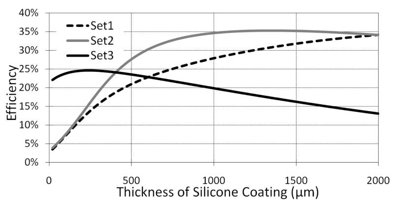
All implantable devices need to be hermetically sealed in a biocompatible material to withstand the harsh environment inside the body without causing an adverse reaction. The receiver coil in inductively powered devices, such as cochlear implants, is often embedded in ceramic, parylene, or medical grade silicone [1]. The dielectric constant, εr, of silicone coating is much lower than saline or any type of human tissue, as shown in Table I. Therefore, increasing the thickness of the coating will reduce CP and increase RP in the PSC model, both of which help increasing Q and consequently η12. On the other hand, increasing the thickness of the coating will increase d and the volume of the implantable device (tissue displacement), both of which are undesired. Nevertheless, we found it instructive to indicate the optimal coating thickness by sweeping t2 in our model (Fig. 2), while maintaining all other parameters constant.
In these model-based simulations, we considered all PSCs in the muscle environment, and maintained the distance between the outer surfaces of the PSC coatings that were facing each other at 10 mm. Also, the thicknesses of the coatings were considered the same for both internal and external PSCs. Hence, the actual coupling distance between the two PSC windings was d = 2t2 + 10 mm.
Fig. 5 shows the results of varying the coating thickness of PSCs in Table II. It can be seen from our model that the optimal thickness for Set-3, which geometries are optimized for the muscle environment, is a reasonable value of t2 = ~300 μm. However, the other PSCs need much thicker coatings to reach their maximum efficiencies. This is because their geometries are optimized for lower loss environments and they need thicker coatings to compensate for the additional loss in the muscle environment. Such thicknesses are obviously not realistic for implantable applications.
Fig. 5.
Optimal thickness of the silicone coating on both sides of each PSC with geometries given in Table II in the muscle environment. The distance between the coating surfaces that face each other is fixed at 10 mm.
IV. Simulation and Measurement Results
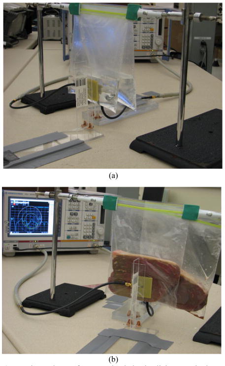
Fig. 6 shows the PSC measurement setup. We have used a network analyzer (R&S ZVB4) to measure the S-parameters of each coupled PSC pair, while they were mounted vertically at a desired coupling distance using Plexiglas supports. The S-parameters were converted to Z-parameters to calculate k and the quality factors from (17)–(21), which were then substituted in (22) to find η12 [29]. In addition to measurements in air, we used two plastic bags (~50 μm thick), hanging from a horizontal clamp, and filled them with saline or beef to emulate implant environments. The internal PSC was sandwiched between the two bags while the external PSC was aligned with it, touching the outer surface of one of the bags (see Fig. 6). The thickness of the layer between PCSs was t1 = 10 mm, and the layers behind the internal PSCs, t3, were 70 mm and 50 mm for saline and beef, respectively. The saline we used was a solution of distilled water and 9 mg/L NaCl. The beef was bovine sirloin steak, which is the muscle cut from the lower portion of the ribs. The beef temperature at the time of measurement was 10.8 °C and the saline was in equilibrium with the room temperature at 24.0 °C.
Fig. 6.
Experimental setup for measuring inductive link properties between a pair of PSCs in the air, saline (a) and muscle (b) environments.
A. PSC Quality Factor
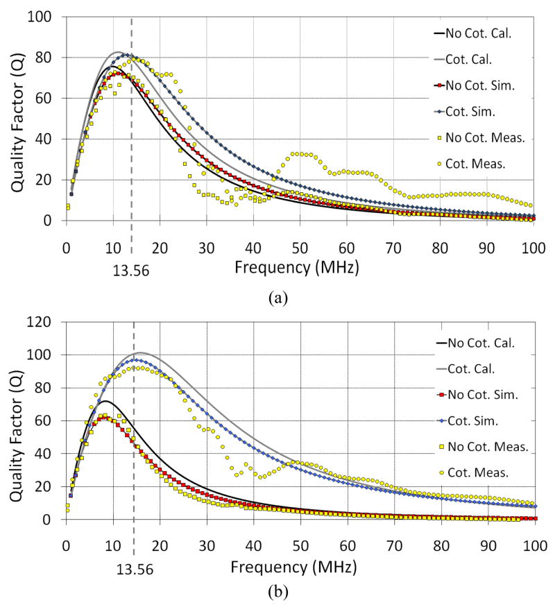
In section III.B we used our PSC models to find the optimal thickness of the silicone coating on the PSCs in the muscle environment. We coated one sample from each PSC pair in Table II with CF16-2186 silicone elastomer from NuSil (Carpinteria, CA) up to a thickness of ~300 μm. Fig. 7 compares the theoretical calculation, HFSS simulation, and measurement results of PSC21 and PSC31 (both external) quality factors vs. carrier frequency, with and without coating, in saline and muscle environments. It can be seen that Q of both PSCs have been improved with the silicone coating as predicted earlier by our model. This improvement is more significant for PSC31, which is coated close to its optimal coating thickness. These curves also show that there is a good agreement among theoretical models, FEA-based simulations (HFSS), and experimental measurement results.
Fig. 7.
Comparison between theoretical calculations, HFSS simulations, and measurement results of Q variations vs. carrier frequency of (a) PSC21 in saline and (b) PSC31 in muscle, with and without 300 μm silicone coating.
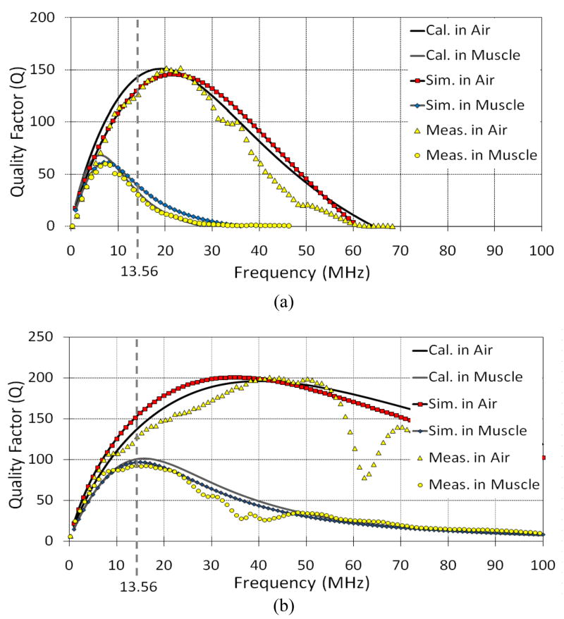
Quality factor of each PSC drops in high permittivity and high conductivity environments, and that leads to higher losses. We evaluated the effects of geometry optimizations in section III.A on the Q of PSCs in each environment. Fig. 8 shows how the Q of coated PSC11 and PSC31 change vs. frequency in the air and muscle environments. PSC11 is optimized for air. Therefore, at 13.56 MHz, its Q decreases by 78% from 128 in air to 28 in the muscle environment due to changes in CP and RP, which also result in significant reduction in PSC11’s SRF. On the other hand, the Q of PSC31 decreases only by 25% from 122 in air to 92 in muscle. The agreement among calculation, simulation, and measurement results in Fig. 8 demonstrate the efficacy of the geometrical optimization algorithm and models described in section II, which have helped to improve the PSC quality factors by a factor of ~3.3 in the muscle environment.
Fig. 8.
Comparison between theoretical calculations, HFSS simulations, and measurement results of Q variations vs. carrier frequency in (a) PSC11 that is optimized for air, and (b) PSC31 that is optimized for muscle, in these two environments (see Table II for PSC geometries).
Optimization of the implanted PSC for the surrounding environment is influenced by the dramatic changes in the geometry of the external PSC. A comparison between PSC12 and PSC32 in Table II shows that optimization for the muscle environment has reduced n32 and w32, both of which reduce CP2 and RP2. In measurements, Q of PSC12 and PSC32 reduced from 51.5 and 36.6 in the air to 42.3 and 36 in the muscle environment, respectively. Even though the optimized PSC12 offers a slightly higher Q than PSC32, it has a weaker coupling to PSC31. This is mainly due to the size constraint applied to the implanted PSC (10×10 mm2). Therefore, the resulting power transfer efficiency in muscle for Set-3 is higher than Set-1, as discussed in section IV.B.
B. Power Transfer Efficiency
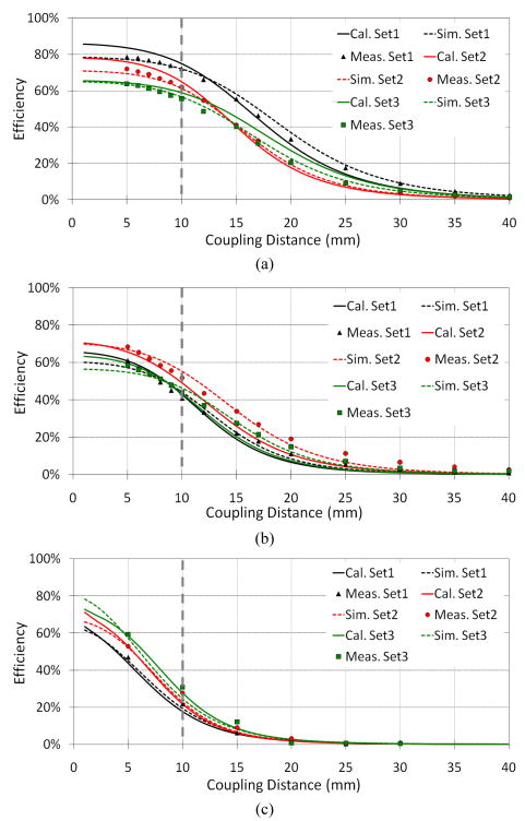
PSC pair geometries affect k and Q, both of which are key factors in η12 according to (22). Here we compare the power transfer efficiency of the 3 sets of PSCs in Table II in the air, saline, and muscle environments, in Figs. 9a, 9b, and 9c, respectively, through model-based theoretical calculations, FEA simulations, and experimental measurements. The PSCs are perfectly aligned and their coupling distance on the horizontal axis includes their coating thickness (300 μm). The carrier frequency is held constant at 13.56 MHz, and the secondary PSC is loaded with RL = 500 Ω.
Fig. 9.
Variations of the power transfer efficiency with coupling distance at 13.56 MHz for three sets of PSCs in Table II optimized for (a) air, (b) saline, and (c) muscle environments.
Fig. 9 curves show that each set of PSCs performs best in its designated operating environment, most important of which is the muscle, where an implantable device eventually resides. Fig. 9c obviously shows that a pair of PSCs that is optimized for air (Set-1) provides the worst η12 when implanted in the muscular tissue. While Set-1 PSC pair can achieve more than 70% efficiency in the air due to their high k, their η12 drops to only 21.8% in the muscle environment due to degradation in their Q, as seen in Fig. 8a. Set-3 pair, on the other hand, provides η12 > 30% at d = 10 mm due to PSC31 smaller geometries, which is optimized for this environment. These results signify the importance of using detailed models in designing implantable PSCs, in which the effects of parasitic components have been taken into account.
Fig. 9 also shows reasonable agreement among theoretical calculations from our models, finite element simulations, and measurement results. There are, however, small discrepancies due to the following reasons, some of which are related to our models and some are related to the measurement setup: 1) inherent limitations in the accuracy of the closed form equations, particularly when the PSC parameters are close to or out of their valid range of parameters, 2) large line width and small number of turns, resulted from our optimization algorithm particularly for Set-3 (Table II), causing the shape of PSC13 to deviate from a perfect square with rounded corners, affecting the validity of (1), 3) secondary effects such fringing and capacitive coupling between the two inductively coupled PSCs, which were not included in our models, 4) manually applied silicone coating was not quite uniformly distributed on the PSC surfaces, 5) there could be small patches of air gap between the plastic bags containing the volume conductors and the outer surface of the PSCs’ silicone coating, and 6) the 50 μm thick plastic bag, made of polyethylene (PE) with εr = 2.3 and tan(δ) = 0.0002, which was considered to be part of the PSC silicone coating.
V. Conclusion
We have constructed detailed models and devised design paradigms for small PSCs that are meant to be fabricated on rigid or flexible planar substrates, coated with biocompatible dielectric materials, such as silicone, and implanted in homogeneous tissue environments. Various phenomena that could result in degradation of the PSC quality factors due to coating and implantation were considered in our models. We combined our models with an iterative PSC design procedure, previously reported in [16], to optimize the PSC geometries for providing maximum power transfer efficiency in tissue environments. This can result in lower heat dissipation, extended battery lifetime, and improved safety in neuroprosthetic devices, such as retinal or cortical implants, with demanding size constraints [30].
We validated the PSC design procedure by applying it to an exemplar 1 cm2 implantable visual prosthesis operating at 13.56 MHz. We constructed finite element analysis models in HFSS using the resulting optimal geometries and simulated them. We also fabricated several PSC pairs on FR4 and conducted experimental measurements in air, saline, and muscle environments. All calculation, simulation, and measurement results were in close agreement within the desired range of design parameters, and demonstrated the validity of the models and proposed iterative PSC design procedure. We are now utilizing the proposed method in design and development of a multi-carrier inductive wireless link for high performance neuroprosthetic devices [31], [32]. We plan to fabricate the optimized PSCs on higher quality substrates with smaller feature size using MEMS technology.
Acknowledgments
The authors would like to thank members of the GT-Bionics lab for their help with the measurements.
This work was supported in part by the National Institute of Health grant 1R01NS062031-01A1, and the National Science Foundation under award ECCS-824199.
Biographies
 Uei-Ming Jow (S’07) received a B.E. degree in electrical engineering from Tatung University, and a M.S. degree in electronic engineering from the National Taiwan University of Science and Technology, in 1999 and 2001, respectively. From 2001 to 2006, he joined Industrial Technology Research Institute at Hsinchu, Taiwan, and worked in Electronics Research & Service Organization as a RF engineer. He was involved in the analysis and design of electromagnetic compatibility for the high speed digital circuit as well as the embedded RF circuit packaging technology.
Since fall 2007, he has been working towards his PhD degree at the Georgia Institute of Technology. His main research interests are neural and bionic implants, the integrated analog circuit design, and wireless implantable biomedical systems.
 Maysam Ghovanloo (S’00 M’04) was born in 1973. He received the B.S. degree in electrical engineering from the University of Tehran, Tehran, Iran, in 1994 and the M.S. degree in biomedical engineering from the Amirkabir University of Technology, Tehran, Iran, in 1997. He also received the M.S. and Ph.D. degrees in electrical engineering from the University of Michigan, Ann Arbor, MI in 2003 and 2004, respectively. His Ph.D. research was on developing a wireless microsystem for neural stimulating microprobes.
From 2004 to 2007 he was an assistant professor at the department of electrical and computer engineering in the North Carolina State University, Raleigh, NC, where he founded the NC-Bionics Lab. In June 2007 he joined the faculty of Georgia Institute of Technology, Atlanta, GA, where he is currently an assistant professor and the founding director of the GT-Bionics Lab in the School of Electrical and Computer Engineering.
Dr. Ghovanloo has received awards in the 40th and 41st DAC/ISSCC student design contest in 2003 and 2004, respectively. He has more than 70 conference and journal publications. He has organized special sessions and served in technical review committees for major conferences and journals in the areas of circuits, systems, sensors, and biomedical engineering. He is a member of Tau Beta Pi, Sigma Xi, and IEEE Solid-State Circuits, Circuits and Systems, and Engineering in Medicine and Biology societies.
References
- 1.Cochlear Corporation. Nucleus Freedom Implant. [Online], Available: http://www.cochlearamericas.com/Products/23.asp.
- 2.Humayun MS, et al. Visual perception in a blind subject with a chronic microelectronic retinal prosthesis. Vision Research. 2003 Nov;43:2573–2581. doi: 10.1016/s0042-6989(03)00457-7. [DOI] [PubMed] [Google Scholar]
- 3.Harrison RR, et al. Wireless neural recording with single low-power integrated circuit. To appear in IEEE Trans Neural Sys Rehab Eng. doi: 10.1109/TNSRE.2009.2023298. [DOI] [PMC free article] [PubMed] [Google Scholar]
- 4.Sokal NO, Sokal AD. Class-E—A new class of high-efficiency tuned single-ended switching power amplifiers. IEEE J Solid-State Circuits. 1975 June;SSC–10(2):168–176. [Google Scholar]
- 5.Yang Z, Liu W, Basham E. Inductor modeling in wireless links for implantable electronics. IEEE Trans Magnetics. 2007 Oct;43(10):3851–3860. [Google Scholar]
- 6.Shah MR, Phillips RP, Normann RA. A study of printed spiral coils for neuroprosthetic transcranial telemetry applications. IEEE Trans Biomed Eng. 1998 July;45:867–876. doi: 10.1109/10.686794. [DOI] [PubMed] [Google Scholar]
- 7.Von Arx JA, Najafi K. A wireless single-chip telemetry-powered neural stimulation system. Digest IEEE Intl. Solid-State Circuits Conf; Feb 1999.pp. 214–215. [Google Scholar]
- 8.Töpper M, et al. Biocompatible hybrid flip chip microsystem integration for next generation wireless neural interfaces. Proc. IEEE Elec. Components Tech. Conf; May 2006.pp. 705–708. [Google Scholar]
- 9.Kim S, Zoschke K, Klein M, Black D, Buschick K, Toepper M, Tathireddy P, Harrison R, Oppermann H, Solzbacher F. Switchable polymer-based thin film coils as a power module for wireless neural interfaces. Sensors Actuators A. 2007 Nov;136:467–474. doi: 10.1016/j.sna.2006.10.048. [DOI] [PMC free article] [PubMed] [Google Scholar]
- 10.Ko WH, Liang SP, Fung CDF. Design of radio-frequency powered coils for implant instruments. Med Biol Eng Comput. 1977;15:634–640. doi: 10.1007/BF02457921. [DOI] [PubMed] [Google Scholar]
- 11.Heetderks WJ. RF powering of millimeter and submillimeter-sized neural prosthetic implants. IEEE Trans Biomed Eng. 1988 May;35:323–327. doi: 10.1109/10.1388. [DOI] [PubMed] [Google Scholar]
- 12.Zierhofer CM, Hochmair ES. Geometric approach for coupling enhancement of magnetically coupled coils. IEEE Trans Biomedical Engineering. 1996 July;43(7):708–714. doi: 10.1109/10.503178. [DOI] [PubMed] [Google Scholar]
- 13.Neagu CR, Jansen HV, Smith A, Gardeniers JGE, Elwanspoek MC. Characterization of a planar microcoil for implantable microsystems. Sensors Actuators A. 1997;62:599–611. [Google Scholar]
- 14.Kendir GA, et al. An optimal design methodology for inductive power link with class-E amplifier. IEEE Trans Circuits and Sys I. 2005 May;52(5):857–866. [Google Scholar]
- 15.Baker MW, Sarpeshkar R. Feedback analysis and design of RF power links for low-power bionic systems. IEEE Trans Biomed Cir and Sys. 2007 Mar;1(1):28–38. doi: 10.1109/TBCAS.2007.893180. [DOI] [PubMed] [Google Scholar]
- 16.Jow U, Ghovanloo M. Design and optimization of printed spiral coils for efficient transcutaneous inductive power transmission. IEEE Trans Biomed Cir Sys. 2007 Sep;1(3):193–202. doi: 10.1109/TBCAS.2007.913130. [DOI] [PubMed] [Google Scholar]
- 17.Finkenzeller K. RFID Handbook: Fundamentals and Applications in Contactless Smart Cards and Identification. 2. Hoboken, NJ: John Wiley & Sons; 2003. [Google Scholar]
- 18.Mohan SS, del Mar Hershenson M, Boyd SP, Lee TH. Simple accurate expressions for planar spiral inductances. IEEE J Solid-State Circuits. 1999 Oct;34(10):1419–1424. [Google Scholar]
- 19.Pieters P, Vaesen K, Brebels S, Mahmoud SF, DeRaedt W, Beyne E, Mertens RP. Accurate modeling of high-Q spiral inductors in thin-film multilayer technology for wireless telecommunication applications. IEEE Trans Microwave Theory Tech. 2001 Apr;49(4):589–599. [Google Scholar]
- 20.Hoffmann RK. Handbook of Microwave Integrated Circuit. Norwood, MA: Artech House; 1987. [Google Scholar]
- 21.Gevorgian S, Berg H, Jacobsson H, Lewin T. Basic parameters of coplanar-strip waveguides on multilayer dielectric/semiconductor substrates, Part 1: high permittivity superstrates. IEEE Microwave Magazine. 2003 June;4(2):60–70. [Google Scholar]
- 22.Wheeler HA. Formulas for the skin effect. Proceedings of the IRE. 1942 Sep;30(9):412–424. [Google Scholar]
- 23.Kuhn WB, Ibrahim NM. Analysis of current crowding effects in multiturn spiral inductors. IEEE Trans Microwave Theory Tech. 2001 Jan;49(1):31–38. [Google Scholar]
- 24.Ulrich RK, Schaper LW. Integrated Passive Component Technology. ch11. Hoboken, NJ: Wiley-IEEE Press; 2003. [Google Scholar]
- 25.Akyel C, Babic S, Kincic S. New and fast procedures for calculating the mutual inductance of coaxial circular coils (circular coil–disk coil) IEEE Trans on Magnetics. 2002 Sep;38(5):2367–2369. [Google Scholar]
- 26.Gabriel S, Lau RW, Gabriel C. The dielectric properties of biological tissues: II. Measurements in the frequency range 10 Hz to 20 GHz. Phys Med Biol. 1996 Nov;41:2251–2269. doi: 10.1088/0031-9155/41/11/002. [DOI] [PubMed] [Google Scholar]
- 27.Kim J, Oh D, Yoon J, Cho S, Kim N, Cho J, Kwon Y, Cheon C, Kim Y. In vitro and in vivo measurement for biological applications using micromachined probe. IEEE MTT, Trans. 2005 Nov;53(11):3415–3421. [Google Scholar]
- 28.Jow U, Ghovanloo M. Optimization of a multiband wireless link for neuroprosthetic implantable devices. Proc. IEEE Biomed. Circuits and Systems; Nov. 2008; pp. 97–100. [DOI] [PMC free article] [PubMed] [Google Scholar]
- 29.Pozar DM. Microwave Engineering. 2. ch 4. New York, NY: John Wiley & Sons; 1998. [Google Scholar]
- 30.Lazzi G. Thermal effects of bioimplants. IEEE Eng in Med Biol Magazine. 2005 Sep;24(5):75–81. doi: 10.1109/memb.2005.1511503. [DOI] [PubMed] [Google Scholar]
- 31.Ghovanloo M, Lazzi G. Transcutaneous magnetic coupling of power and data. In: Akay Metin., editor. Wiley Encyclopedia of Biomedical Engineering. Hoboken, NJ: Wiley; Apr, 2006. [Google Scholar]
- 32.Ghovanloo M, Atluri S. A wideband power-efficient inductive wireless link for implantable microelectronic devices using multiple carriers. IEEE Trans. on Circuits and Systems I; May 2006.pp. 21–24. [Google Scholar]
- 33.Bahl IJ, Garg R. Simple and accurate formulas for a microstrip with finite strip thickness. Proc IEEE. 1977 Nov;65(11):1611–1612. [Google Scholar]


