Fabricating electronic devices using multi-level photolithography provides excellent control of feature geometry and registration between layers (1), but each deposition step incorporates just one material, from a limited set, over the entire chip. Alternatively, device components such as nanowires can be synthesized from many different materials and even coated with biological molecules before assembling them onto a chip. However, it is still challenging to accurately position the various nanowires in different locations on the chip (2, 3).
We present a hybrid approach that uses forces generated by electric fields to direct different populations of biofunctionalized nanowires to specific regions of the chip while providing accurate registry between each individual nanowire and the photolithographic features within that region. We synchronized sequential injections of nanowires carrying different DNA sequences with a programmed, spatially confined electric-field profile that directs nanowire assembly. Nanowire-bound DNA was able to selectively bind complementary targets after assembly and device fabrication, which makes this process compatible with conventional integrated circuit manufacturing.
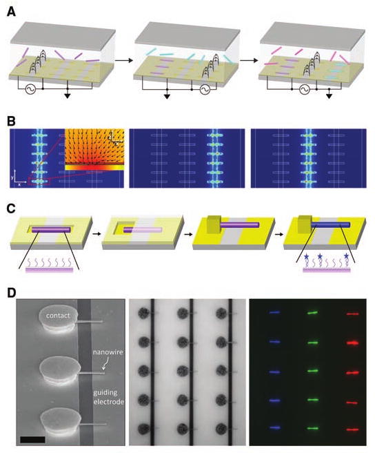
DNA oligonucleotides complementary to sequences found in human pathogens were attached covalently to different batches of nanowires (8 μm long, ∼109 wires per ml) (4). Aliquots were sequentially injected across a dense two-dimensional array of photolithographically defined microwells superimposed across gaps separating guiding electrodes used for programmed assembly (Fig. 1A). Electric-field calculations with sinusoidal voltages applied between specific pairs of guiding electrodes showed that the field strength is highest in the microwells that span the biased electrodes and negligible elsewhere (Fig. 1B). These field gradients induced long-range dielectrophoretic forces that directed individual nanowires to the biased microwells in <1 min. Fields were shielded in occupied wells, preventing additional nanowires from entering. Electrostatic forces centered the wires across the gaps, and capillary forces pushed them against the sides of the wells; this fixed the position of nanowire tips and their pitch, respectively. After all batches were assembled, we generated an array of nanowire resonator devices (5) by forming contacts to each wire (Fig. 1C).
Fig. 1.

Fabrication of multisequence DNA-coated nanowire device array. (A) Assembly process. Suspensions of nanowires carrying different DNAs were injected sequentially, while 4.2-V, 1-MHz voltages were applied between guiding electrodes. Nanowires were directed to microwells in a particular column. (B) Simulated spatial electrical-field gradient during assembly. Contour plots show ▽|E|2 measured at the surface of the microwells for the peak value of voltage applied in (A), where E is the electric field; scale is 1010 (blue) to 1018 (red) V2/m3. (Inset) Cross-sectional view of one microwell, plotted as log▽|E|2; scale is 1013 (yellow) to 1020 (red) V2/m3; arrows indicate the dielectrophoretic force. (C) Postassembly device integration. Windows registered to microwells were opened in photoresist. Au contacts were electrodeposited; additional processing, for example, oxide removal, is possible. Dissolving photoresist left nanowire resonator devices; these were incubated with DNA. (D) Scanning electron microscope (left), optical reflectance (center), and fluorescence (right) images after incubation with labeled complementary targets. Scale bar indicates 5 μm.
In this proof of concept, we assembled nanowires carrying different DNA sequences into three separate columns. We used ∼300-nm-diameter wires, with a 20-nm SiO2 shell to facilitate verification of DNA function by fluorescence. After device integration, the entire chip was incubated with a mixture of DNA target sequences, each complementary to one of the nanowire-bound probes and labeled with a different dye. Each labeled target bound to wires in a different column (Fig. 1D), indicating successful nanowire assembly and retention of DNA binding selectivity despite exposure to electric fields, photoresist coatings, and solvents.
Almost no nanowires assembled in the wrong column (≤1%). The array had a 71% yield of individual nanowire devices in 750 potential sites (2.4 × 10⁴ devices per cm2); defects included vacancies (19%) and multiples of the same nanowire type (9%). Submicrometer placement accuracy was achieved across the entire array. This would allow direct electrical connection between each nanowire device and a dedicated transistor on an integrated circuit chip. This assembly approach, which is also compatible with smaller-diameter nanowires, could be extended to more diverse materials or coatings and alternative device structures, such as field effect transistors that enable not only detection but also stimulation of biological events (6, 7).
Supplementary Material
Acknowledgments
Supported by NIH, NSF, and Semiconductor Research Corporation–Nanoelectronics Research Initiative.
Footnotes
Supporting Online Material: www.sciencemag.org/cgi/content/full/323/5912/352/DC1
Materials and Methods
References
References and Notes
- 1.Ito T, Okazaki S. Nature. 2000;406:1027. doi: 10.1038/35023233. [DOI] [PubMed] [Google Scholar]
- 2.Ahn JH, et al. Science. 2006;314:1754. doi: 10.1126/science.1132394. [DOI] [PubMed] [Google Scholar]
- 3.Lu W, Lieber CM. Nat Mater. 2007;6:841. doi: 10.1038/nmat2028. [DOI] [PubMed] [Google Scholar]
- 4.Materials and methods are available as supporting material on Science Online.
- 5.Li M, et al. Nat Nanotechnol. 2008;3:88. doi: 10.1038/nnano.2008.26. [DOI] [PMC free article] [PubMed] [Google Scholar]
- 6.Patolsky F, et al. Science. 2006;313:1100. doi: 10.1126/science.1128640. [DOI] [PubMed] [Google Scholar]
- 7.Ho TT, et al. Nano Lett. 2008;8:4359. doi: 10.1021/nl8022059. [DOI] [PubMed] [Google Scholar]
Associated Data
This section collects any data citations, data availability statements, or supplementary materials included in this article.


