Abstract
Piezoresistive silicon cantilevers fabricated by ion implantation are frequently used for force, displacement, and chemical sensors due to their low cost and electronic readout. However, the design of piezoresistive cantilevers is not a straightforward problem due to coupling between the design parameters, constraints, process conditions, and performance. We systematically analyzed the effect of design and process parameters on force resolution and then developed an optimization approach to improve force resolution while satisfying various design constraints using simulation results. The combined simulation and optimization approach is extensible to other doping methods beyond ion implantation in principle. The optimization results were validated by fabricating cantilevers with the optimized conditions and characterizing their performance. The measurement results demonstrate that the analytical model accurately predicts force and displacement resolution, and sensitivity and noise tradeoff in optimal cantilever performance. We also performed a comparison between our optimization technique and existing models and demonstrated eight times improvement in force resolution over simplified models.
Index Terms: Force sensor, optimization, piezoresistance, piezoresistive cantilever
I. Introduction
Piezoresistive silicon cantilevers have become increasingly popular as force and displacement sensors [1], since the first piezoresistive atomic force microscope cantilevers developed by Tortonese et al. [2]. Piezoresistors have advantages such as high dynamic range [3], relatively small size, simple fabrication, and straightforward signal-conditioning circuitry.
However, piezoresistor design remains challenging due to the many coupled parameters such as cantilever and piezoresistor dimensions and also fabrication process parameters such as implantation energy and dose, annealing time and temperature, and bias voltage, which must be chosen carefully to optimize the performance given a set of constraints such as measurement bandwidth, stiffness, and power dissipation (Table I). For example, a reduction in piezoresistor dopant concentration leads to increased sensitivity but increased noise, and the effect on overall performance depends upon the constraints and operating conditions of the piezoresistor.
TABLE I.
Design Matrix Showing Relationship of Parameters for Performance in Piezoresistive Cantilevers. As the Controlled Design Parameter Increases (While Other Parameters are Held at Typical Values), the Observed Parameters Respond as Follows: Increasing(↑), Decreasing(↓), and Weak or No Relation (-). p, Vbridge, and are Dopant Concentration, Bridge Voltage, and Diffusion Length, Respectively. lc, wc, and tc, are the Cantilever Length,Width, and Thickness, Respectively. lp, wp, and tp are the Piezoresistor Length,Width, and Thickness, Respectively (Adapted from [2])
| Observed parameters | |||||
|---|---|---|---|---|---|
| Sensitivity (V/N) | 1/f noise | Johnson noise | |||
| Controlled parameters | ↑ | p (cm−3) | ↓ | ↓ | ↓ |
| ↑ | Vbridge (V) | ↑ | ↑ | - | |
| ↑ |
|
↓ | ↓ | ↓ | |
| ↑ | lc(m) | ↑ | - | - | |
| ↑ | wc(m) | ↓ | - | - | |
| ↑ | tc(m) | ↓ | - | - | |
| ↑ | lp(m) | ↓ | ↓ | ↑ | |
| ↑ | wp(m) | - | ↓ | ↓ | |
| ↑ | tp(m) | ↓ | ↓ | ↓ | |
Many researchers have focused on improving the resolution of piezoresistive cantilevers [4]–[8]. However, prior works have considered a limited number of design and process parameters. Harley and Kenny [5], Yu et al. [6], and Wang et al. [8] demonstrated the optimized design of piezoresistive cantilevers only for epitaxial piezoresistors, where the dopant concentration is constant through the thickness of the piezoresistor [9]. Although piezoresistors are commonly fabricated by ion implantation due to low cost and wide availability, an epitaxial optimization approach is not accurate when the dopant profile is not uniform.
In this paper, we demonstrate the choice of optimal design parameters that satisfy the complex parameter interaction of ion-implanted piezoresistive cantilevers. Previously, we reported an improved analytical model for the sensitivity of piezoresistors with arbitrary dopant profiles [10], [11]; however, the effect of noise was not considered. Here, we simulate the dopant profile for various design conditions and analyze the overall cantilever force and displacement resolution performance. We also implement an optimization technique to consider the design constraints in arriving at an optimized cantilever design. Finally, we designed, fabricated, and characterized cantilevers to validate the optimization method. The optimization technique presented is based upon standard process simulation methods and is directly applicable to piezoresistive transducers fabricated with other methods, such as epitaxial growth and diffusion, and is extensible to the design of other piezoresistive devices.
II. Methods
Piezoresistive silicon cantilevers were fabricated for validation of the optimization technique. We have previously reported the fabrication process [12]–[14]. Briefly, the cantilevers were fabricated from silicon-on-insulator (SOI) wafers with a 7-μm device layer and 300-nm buried oxide (IceMos Technology, Belfast, U.K.) using a 7-mask process (Fig. 1). The piezoresistors (length lp : 50–316 μm; width wp : 8.5 μm) were formed by boron ion implantation, and the cantilevers (length lc : 2 mm; width wc : 30 μm) were accordingly oriented in the 〈110〉 direction (E = 169 GPa) to maximize the longitudinal piezoresistivity. We processed two SOIs with optimized conditions and eight others with varied process conditions for comparison. Individual devices were attached to custom printed circuit boards (PCBs) (Imagineering Inc., Elk Grove Village, IL) with epoxy (Devcon, Glenview, IL) and wirebonded with aluminum wire (Fig. 2). The strained piezoresistor is located on the cantilever, and three other unstrained piezoresistors with matched resistance are on the same die for temperature compensation.
Fig. 1.
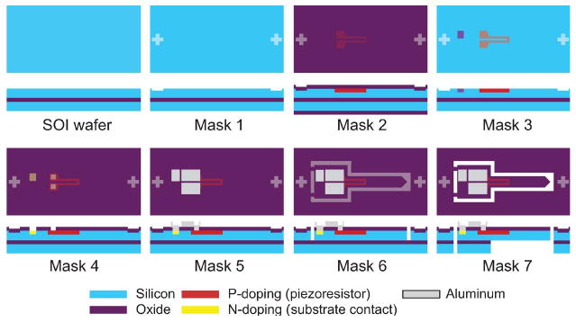
Piezoresistive cantilever fabrication process. (Mask 1) Pattern alignment marks. (Mask 2) Grow 250-Å screening wet oxide at 850 °C for 13 min, and pattern piezoresistors; then, ion implant 2 · 1014, 2 · 1015, 5 · 1015, and 1016-cm−2 boron for the piezoresistor regions. (Mask 3) Pattern n++ region, and ion implant 5 · 1015-cm−2 arsenic for substrate contact; then, etch damaged oxide in 6 : 1 buffered oxide etch (BOE). (Mask 4) Grow isolation wet oxide at 1000 °C– 1150 °C (15–45 min) plus 1000 °C–1150 °C inert N2 anneal (5–32 min); then, pattern and wet etch (6 : 1 BOE) contact vias through the oxide. (Mask 5) Sputter 1 μm of 99% Al/1% Si; then, pattern and wet etch (Olin Aluminum Etch II) the Al. (Mask 6) Pattern cantilevers, and etch the oxide and silicon with 6:1 BOE, then deep reactive ion etch (DRIE) stopping on the buried oxide layer. (Mask 7) Leave front-side resist, and release the cantilevers using back-side pattern alignment, then a DRIE process stopping on the buried oxide again; remove buried oxide from cantilevers using RIE, and finally anneal the wafers in H2 forming gas at 475 °C (10 min) to improve contact resistance and noise.
Fig. 2.
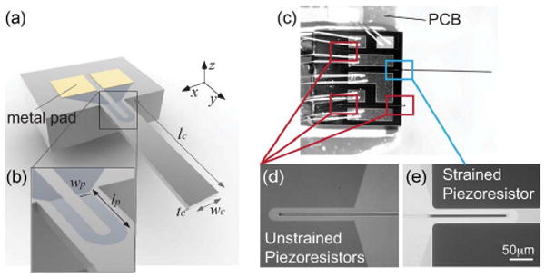
Piezoresistive microcantilever. (a) Geometry of cantilever. (b) Geometry of piezoresistor. (c) A 30-μm-wide 2000-μm-long cantilever having 8.5-μm-wide 153-μm-long U-shaped piezoresistor with 5-μm gap. The devices were directly attached to custom PCBs. The (e) strained piezoresistor is located on the cantilever, and (d) three other unstrained piezoresistors are physically on the same die for temperature compensation.
We measured the spring constant, force sensitivity, and first-mode resonant frequency of each cantilever using a Laser Doppler Vibrometer (Polytec OFV3001), a signal analyzer (HP 89441A), and a piezoelectric shaker (Jodon, Ann Arbor, MI) as described previously [12]. For noise characterization, we used a Wheatstone bridge with two signal conditioning circuits (Fig. 3). Johnson noise was measured with a simple instrumentation amplifier circuit (INA103, Texas Instruments, U.S.) with dc bias. The Johnson noise floor of the INA103 is excellent ; however, its 1/f noise is greater than that of the piezoresistors we tested. Therefore, we used an ac bridge circuit [Fig. 3(b)] with 600-Hz ac modulation signal, which is greater than the 1/f corner frequency of the INA103, to remove 1/f noise of the instrumentation amplifier. The low-frequency signal from the piezoresistive cantilever is recovered at the output of a bandpass filter (bandwidth of 200 Hz and center frequency of 600 Hz), a synchronous demodulator (AD630, Analog Devices, U.S.), and a low-pass filter (cutoff frequency of 100 Hz) [3].
Fig. 3.
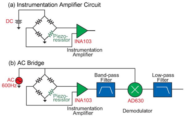
(a) Measurement circuit for Johnson noise utilizes a standard Wheat-stone bridge and instrumentation amplifier. (b) Measurement circuit for piezoresistor 1/f noise adds 600-Hz modulation and demodulation to remove the 1/f noise of the amplifier. Note that three unstrained piezoresistors are used for the other three legs of the Wheatstone bridge for temperature compensation. (a) Instrumentation amplifier circuit. (b) AC bridge.
We calculated the efficiency factor β*, the number of dopant atoms across the piezoresistor thickness Nz, and sheet resistance Rs based upon the simulation results from TSUPREM4 (Synopsys, Mountain View, CA). We simulated the fabrication process given in Table II and compared the simulation results with dopant profiles measured by spreading resistance analysis (Solecon Laboratories, Reno, NV) of test structures (200 μm × 2 mm).
TABLE II.
Process Parameters of TSUPREM4 Simulation
| Process | Parameters |
|---|---|
| Screening 250 Å oxide growth | wet O2 and 850°C for 17 min |
| Ion implant with boron | 1014 to 5 · 1016 cm−2, 50 keV energy, 7° tilt |
| Strip screening oxide | all |
| 1500 Å oxide growth | wet O2 or dry O2, 900 to 1150°C |
| Inert N2 anneal | 900 to 1150°C for 1 to 900 min |
| Forming gas anneal | 475°C for 10 min with 96% N2 and 4% H2 |
III. Design Considerations
A. Sensitivity
We previously developed an analytical model for a piezoresistive cantilever (length lc, width wc, and thickness tc) with a U-shaped piezoresistor (length lp and width wp) (Fig. 2) [10]. We assume that the cantilever is much longer than its width and thickness (l ≫ w ≫ t) so that transverse stress can be neglected and Euler beam theory is applicable. Force sensitivity in terms of output voltage from the 1/4-active Wheatstone bridge is
| (1) |
Displacement sensitivity is
| (2) |
where πl,max is the maximum longitudinal piezoresistivity at 300 K, E is Young's modulus in the longitudinal direction of the cantilever, Vbridge is the Wheatstone bridge bias voltage, and γ is a geometric factor defined as the ratio of the resistance of the strained region in the piezoresistor to the total resistance including unstrained regions, interconnects, and contact pads. β* is an efficiency factor defined by
| (3) |
where q, μ, p, and P are the elementary charge, carrier mobility, dopant concentration, and longitudinal piezoresistance factor, respectively. Carrier mobility is a function of dopant concentration and is calculated from [15]. The piezoresistance factor as a function of dopant concentration is calculated from Richter's analytical model [16]. Fig. 4 shows β* for a 7-μm-thick device with 150-nm oxide. To investigate how diffusion affects β* with various process conditions, β* in Fig. 4 was also calculated with various annealing conditions (temperature T and time t) and was plotted in terms of diffusion length . The diffusion coefficient is defined as D = Dio exp(−Eia/kBT), where, for boron, Dio = 0.037 cm2/s and Eia = 3.46 eV [17]. Each line corresponds to each annealing temperature plot with various times (1–900 min).
Fig. 4.
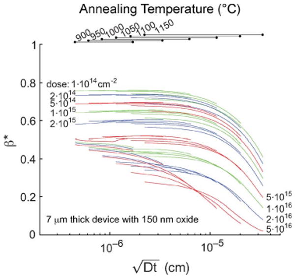
Efficiency factor β* of a 7-μm-thick device with 150-nm oxide. The efficiency factor captures the reduction in sensitivity due to the dopant atoms being spread across the thickness. β* was also calculated with various annealing conditions (temperature and time) and was plotted in terms of diffusion length . Each line corresponds to each annealing temperature plot with various times (1–900 min).
B. Noise
There are two main noise sources that we considered: Hooge noise and Johnson noise [2], [3], [5], [18].
1) Hooge Noise
Hooge noise is a form of 1/f noise related to the finite number of carriers in the piezoresistor. The noise power spectral density is inversely proportional to frequency, and there is a corner frequency, dependent on device design, below which Hooge noise is the dominant noise source. The integrated voltage noise power of Hooge noise for the Wheatstone bridge with four matched piezoresistors is
| (4) |
where α is an empirical parameter related to crystal lattice quality. In ion-implanted cantilevers, α has empirically been found to decrease with diffusion length as α = (1.5 · 10−9)/(Dt)0.25 [3], [5]. fmin and fmax define the measurement bandwidth. The contributions of the piezoresistor U-turn to the number of carriers and resistance are neglected because we assume that lp ≫ wp. We assume that the dopant profile varies only across the thickness of the piezoresistor so that the total number of carriers can be calculated by integrating the dopant atom concentration across the thickness, i.e., . In an epitaxial process, where the dopant profile approximates a step function, Nz is ptp. For ion implantation, Nz is numerically integrated from TSUPREM4 simulation results, as shown in Fig. 5, or spreading resistance analysis.
Fig. 5.
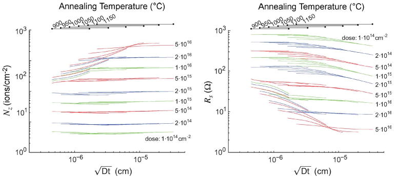
Number of dopant atoms across the thickness of the cantilever and the resulting sheet resistance for ion-implanted piezoresistors. When the concentration is below the solid solubility limit, Nz and Rs slightly decrease with diffusion length, because the dopant atoms diffuse away from the piezoresistor region. However, when the initial concentration is greater than the solid solubility limit at the processing temperature utilized, Nz increases, but Rs decreases with diffusion length because additional dopant atoms are incorporated into the crystal lattice as the local concentration decreases. Each line corresponds to each annealing temperature plot with various times (1–900 min).
2) Johnson Nois
At frequencies above the 1/f corner frequency, Johnson noise is the dominant noise source and is generated by the thermal energy of the carriers in the piezoresistor. Johnson noise is independent of frequency. The Johnson noise of the Wheatstone bridge is equal to the Johnson noise of the piezoresistor when all four resistors are chosen to have the same resistance. In a U-shaped piezoresistor with total resistance, i.e., Rpiezo = 2Rslp/wp, where Rs is the sheet resistance, the integrated Johnson noise power is
| (5) |
For an ideal epitaxial process, Rs= 1/μqptp. In an ion implantation process, we calculate Rs using TSUPREM4 (Fig. 5).
C. Force Resolution
The electrical noise and force sensitivity of the piezoresistive cantilever determine the minimum detectable force or force resolution. From (1), (4), and (5), the force resolution is
| (6) |
where the numerator is the root-mean-square voltage noise and the denominator is the force sensitivity. Force resolution has several factors: cantilever dimensions (lc, wc, and tc), piezoresistor dimensions (lp, wp, and γ), fabrication process parameters (Nz, Rs, α, β, and γ), and operating parameters (Vbridge, T, fmin, and fmax).
The force resolution of an ideal epitaxial piezoresistive cantilever is calculated by replacing β*, Nz, and Rs with P(1 − tp/tc), ptp, and 1/μqptp, respectively. In an ion-implanted cantilever, we calculate the force resolution by using the dopant concentration profile which can be simulated or measured experimentally. Fig. 6(a) shows the simulated force resolution of a typical cantilever with constant bias voltage. The force resolution decreases with increasing diffusion length until the reduction in sensitivity is greater than the reduction in noise. For a fixed bias voltage, the force resolution can be improved by increasing the implantation dose; however, the piezoresistor power dissipation must be considered [Fig. 6(b)].
Fig. 6.

Simulated force resolution of a 2000-μm-long, 30-μm-wide, and 7-μm-thick ion-implanted cantilever with a 350-μm-long, 15-μm-wide, and 50-keV boron-implanted piezoresistor. (a) Force resolution and (b) power with constant bridge voltage (10 V). (c) Force resolution and (d) bridge voltage with constant dissipation power of piezoresistor (25 mW). While a larger dopant dose achieves improved force resolution in the constant bias voltage case, there is an intermediate dose which is optimal in the constant power dissipation case. In the general case, the optimal dose for fixed power dissipation will depend upon the power dissipation, cantilever dimensions, piezoresistor dimensions, and measurement bandwidth. Each line corresponds to each annealing temperature plot with various times (1–900 min).
D. Power Dissipation
Force resolution improves with power dissipation, which can be shown by dividing the numerator and denominator of (6) by Vbridge to obtain
| (7) |
where W is the power dissipated in the piezoresistor . We can improve the force resolution by increasing W up to a threshold value, beyond which there is a negligible improvement in performance with additional power. However, there is a limit to the maximum power dissipation sustainable by the cantilever because Joule heating can destroy the piezoresistor and large bias voltages lead to large leakage currents. Thus, we achieve the optimal force resolution by increasing the power dissipation to the maximum which the cantilever can sustain.
The maximum practical power dissipation depends on the cantilever and piezoresistor dimensions. Due to the high thermal conductivity of silicon, the dominant heat transfer mechanism for a cantilever in air is likely to be conduction rather than convection. The maximum power dissipation is roughly proportional to cantilever thickness and width and inversely proportional to piezoresistor length. For example, a 100-nm-thick cantilever was destroyed with power dissipation in excess of 2–3 mW [5], while we have tested our cantilevers (7 μm thick) to a power dissipation of 25 mW without detriment. Additional experiments and modeling are necessary to more thoroughly investigate the effect of power dissipation on device performance.
We calculated the force resolution of a typical cantilever for various implant doses and constant power (25 mW) in Fig. 6(c). The optimal performance is achieved for a moderate dose (1015−5 · 1015 cm−2) and diffusion length (5 · 10−6 cm). While a larger dopant dose achieves improved force resolution for a constant bias voltage case, an intermediate dose is optimal in the constant power dissipation case. In the general case, the optimal dose for fixed power dissipation will depend upon the power dissipation, cantilever dimensions, piezoresistor dimensions, and measurement bandwidth.
E. Spring Constant
The spring constant is determined by the dimensions of the cantilever and elastic modulus of the cantilever (E)
| (8) |
Force and displacement sensitivities are related to the spring constant: While force sensitivity is inversely proportional to the stiffness, displacement sensitivity is proportional to the stiffness. A soft cantilever deflects more than a stiff cantilever for the same applied force and has better force sensitivity, while a stiff cantilever experiences greater stress than a softer cantilever for the same deflection and has better displacement sensitivity. A final consideration is that, when measuring material properties with a cantilever, cantilever stiffness should typically be comparable to that of the sample in order to sufficiently deform it without damaging it, but the ideal cantilever stiffness may depend upon other considerations as well, such as actuator displacement resolution.
F. Resonant Frequency
The cantilever frequency response is attenuated above the frequency of its first resonant mode. Therefore, the resonant frequency determines the upper limit of the measurement bandwidth. The resonant frequency of cantilever is
| (9) |
where ρs is the density of the cantilever.
G. Dynamic Range
The tip displacement and the applied force are calculated by measuring change in voltage and by assuming that the tip deflection, piezoresistivity, and Wheatstone bridge are linear. However, nonlinear effects become significant for large cantilever deflections. To determine the dynamic range of a piezoresistive cantilever, we compare nonlinearities of three sources: cantilever mechanics, piezoresistivity, and Wheatstone bridge.
1) Structural Nonlinearity
For small deflections, the deflection of the cantilever can be approximated using linear Euler beam theory because geometric nonlinearity is negligible [19], [20]. Belendez et al. [21] derived a differential equation for the force–deflection curve in the general case of large deflections by considering geometric nonlinearity. We solved the nonlinear equations numerically using MATLAB (Mathworks, Cambridge, MA). The difference between a linear model based on the Euler beam theory and the nonlinear models depends on a nondimensional force, i.e., [21]. We can estimate the maximum allowable force for a given degree of nonlinearity from
| (10) |
where Fmaxst is the maximum allowable force. A nonlinear deviation of 0.1% or 1% corresponds to ξst = 0.047 or 0.15, respectively. The maximum forces for the dimensions given in Table III correspond to 3.4 and 10.8 μN for 0.1% and 1% nonlinearities, respectively.
TABLE III.
Design Parameters and Specification of an Example Cantilever with 0.05-N/m Stiffness, 2.5-kHz Resonant Frequency Operating at 1–1000-Hz Frequency, Less Than 2-mW Power Dissipation, and Less Than 2-V (Simulation) and 2.85-V (= Vbridge, max/γ, Measurement) Bridge Voltages
| Target | Optimal devices | Non-optimal devices for comparison | ||||||||||
|---|---|---|---|---|---|---|---|---|---|---|---|---|
| Wet | Dry | ← High sensitivity | Low noise → | |||||||||
| lc×wc (μm) | 2000×30 | |||||||||||
| tc (μm) | 7.0 | 7.1 | 7.3 | 7.4 | 7.3 | 6.7 | 6.8 | 7.2 | 7.4 | 6.9 | 7.7 | |
| lp (μm) | 57 | 50 | 50 | |||||||||
| wp (μm) | 8.5 | 8.5 | 8.5 | |||||||||
| tp (μm) | 2.17* | 1.53 | 1.71 | 0.57 | 1.50 | 1.70 | 1.01 | 2.58 | 2.28 | 1.67 | 4.39 | |
| Implantation dose (cm−2) | 5 · 1015 | 5 ·1015 | 5 · 1015 | 2·1014 | 2 · 1014 | 2 · 1015 | 5 ·1015 | 5 · 1015 | 5 ·1015 | 1016 | 1016 | |
| Anneal temp. (°C) | 1000 | 1000 | 1000 | 900 | 1050 | 1050 | 1000 | 1050 | 1050 | 1000 | 1100 | |
| Oxidation time (min) | 15 | 15 Wet | 310 Dry | 66 Wet | Wet | Wet | 15 Wet | 175 Wet | Wet | 15 Dry | Wet | |
| N2 Anneal time (min) | 300 | 300 | 1 | 1 | 225 | 150 | 10 | 75 | 270 | 180 | 360 | |
|
|
.0374 | .0374 | .0372 | .0045 | .0584 | .0481 | .0105 | .0605 | .0638 | .0294 | .1270 | |
| Rpiezo (Ω) | 500 | 667 | 838 | 8685 | 6210 | 1329 | 697 | 687 | 608 | 345 | 307 | |
| γ | 1 | 0.70 | 0.70 | |||||||||
| Vbridge (V) | 2 | 2.31 | 2.59 | 2.85 | 2.85 | 2.85 | 2.36 | 2.34 | 2.21 | 1.66 | 1.57 | |
| W (mW) | 2 | 2 | 0.23 | 0.33 | 1.53 | 2 | ||||||
| β* | 0.49 | 0.64 | 0.61 | 0.84 | 0.86 | 0.70 | 0.65 | 0.66 | 0.57 | 0.52 | 0.48 | |
| SFV (V/N) | 1414 | 1455 | 1730 | 2420 | 2511 | 2537 | 1604 | 1468 | 1380 | 958 | 763 | |
| Noise (nV) | 96.3 | 105.5 | 120.7 | 1226 | 592 | 158 | 111.9 | 107.7 | 104.7 | 95.4 | 75.2 | |
| Experimental Fmin (PN) | N/A | 72.5 | 69.8 | 506.6 | 235.8 | 62.3*** | 69.8 | 73.4 | 75.9 | 99.6 | 98.5 | |
| Theoretical Fmin (pN)** | 68.1 | 68.6 | 73.3 | 503.7 | 248.6 | 63.5 | 68.2 | 76.7 | 73.6 | 73.3 | 102.0 | |
TSUPREM4 simulation
Theoretical Fmin is based on actual cantilever thickness and dopant profile by spreading resistance analysis.
The device actually had the best force resolution due to its thin cantilever thickness.
2) Piezoresistivity Nonlinearity
Piezoresistivity is linear for small deformations but can be expanded according to
| (11) |
where πi is the ith-order longitudinal piezoresisitivity. Matsuda et al. [22] and Chen and MacDonald [23] estimated nonlinear piezoresistivity by measuring n-type piezoresistivity in large deformation. Based on the third-order model of Chen and MacDonald [23], nonlinear deviations of 0.1% and 1% occur at stresses ξpr = 15.3 and 139 MPa, respectively. Considering stress at the root of cantilever, we can estimate the maximum force (Fmaxpr) to generate 0.1% or 1% nonlinear piezoresistivity with
| (12) |
The maximum forces for the dimensions of cantilever given in Table III correspond to 1.87 and 17.0 μN for 0.1% and 1% nonlinearities, respectively.
3) Wheatstone Bridge Nonlinearity
As in the cases of structural and piezoresistive nonlinearity, a Wheatstone bridge can only be approximated as linear for small outputs. The output voltage is
| (13) |
Nonlinear deviation of 0.1% and 1% occurs at ratio of resistance change, ξwh = 0.002 and 0.02, respectively. From the force sensitivity equation, we can estimate the maximum allowable force for a given nonlinearity from
| (14) |
We can estimate the force (Fmax wh) required to generate 0.1% or 1% nonlinear deviation, which corresponds to 0.8 or 8.8 μN for the dimensions of cantilever given in Table III.
Considering the force resolution of the cantilever used for these calculations (71.2 pN), the dynamic range over which 1% nonlinearity is maintained is greater than 50 dB and is limited by the Wheatstone bridge.
H. Other Considerations
The piezoresistor resistance is constrained by several nonidealities of the instrumentation amplifier chosen for the piezoresistor conditioning circuit. The piezoresistor Johnson noise, which is lower than that of the amplifier, does not improve the overall performance, so the piezoresistor resistance should be at least 100 Ω in the case of the INA103. In addition, the input current noise of the amplifier and the maximum available bias voltage must be considered, both of which limit the maximum resistance to a few kiloohms. Finally, piezoresistivity is a function of temperature, and the temperature dependence is significantly greater for low concentrations, favoring a high implant dose in order to achieve a low temperature coefficient of resistivity [2], [24].
IV. Optimization
To optimize the performance of piezoresistive cantilevers, we should choose design parameters to achieve the best resolution within the constraints discussed in the previous section. Here, we demonstrate the choice of parameters to optimize piezoresistive cantilever performance within a set of imposed constraints. There are four parameter types: cantilever dimensions, piezoresistor dimensions, bias voltage, and fabrication process parameters (implant dose and energy, dopant atom, and annealing time and temperature). We summarize the optimization process, which was performed iteratively in Matlab, in Fig. 7.
Fig. 7.
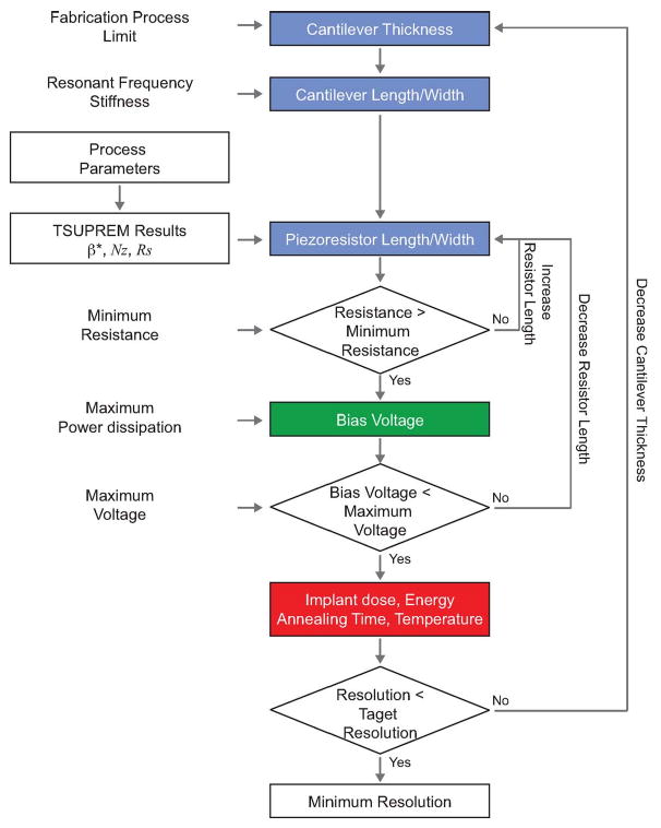
Optimization flowchart. The optimal cantilever dimensions are chosen by the measurement bandwidth and desired stiffness of cantilever. The optimal piezoresistor dimensions require process parameters which have not been selected yet. Thus, we can calculate the local optimal piezoresistor lengths based on simulation results (β*, Rs, and Nz) for a variety of process conditions at first and determine the global optimal piezoresistor length after determining the global optimal process parameters.
A. Cantilever Dimensions
Thickness is based upon the fabrication process constraints. Fabrication of cantilevers less than a micrometer thick using ion implantation is challenging because of the diffusion during the anneal required to electrically activate the dopant atoms and reduce lattice damage (α). Submicrometer cantilevers can be fabricated using epitaxial growth or diffusion [9], [25].
Once cantilever thickness is chosen, the measurement bandwidth and desired stiffness of the cantilever determine the cantilever length and width. The maximum bandwidth is usually limited by the resonant frequency (f0) of the cantilever. The stiffness (kc) of the cantilever is typically determined by the sample being probed, as described earlier.
We can determine the optimal cantilever length and width using stiffness (8), the desired bandwidth (9), and cantilever thickness
| (15) |
| (16) |
Fig. 8 suggests lengths of silicon cantilevers over a range of resonant frequency and thickness for operation in air.
Fig. 8.
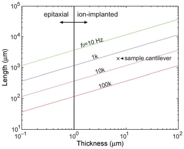
Relationship between piezoresistive cantilever length, thickness, and target resonant frequency (bandwidth). Our sample cantilever is 2000 μm long and 7 μm thick and has a resonant frequency of 2.5 kHz.
B. Piezoresistor Dimensions
Piezoresistor thickness is determined once we select the fabrication process, while piezoresistor length and width are chosen to optimize the force resolution.
1) Optimal Piezoresistor Width
Force resolution is inversely proportional to the piezoresistor width (6). Therefore, we select a piezoresistor width as large as possible (wp = wc/2). Practically, we also consider lithographic tolerance and a minimum gap in the U-shaped piezoresistor.
2) Optimal Piezoresistor Length
The choice of piezoresistor length is not straightforward: While a longer piezoresistor is better for 1/f noise, a shorter piezoresistor is better for Johnson noise and force sensitivity (6). The optimal ratio of the cantilever and piezoresistor length (a = lp/lc) can be found by differentiating the force resolution with respect to a. The optimal length ratio aopt is a function of a characteristic number ψ (Fig. 9)
Fig. 9.
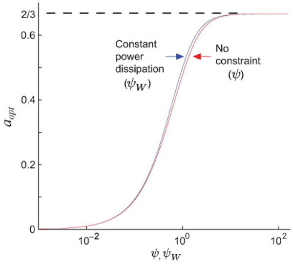
Optimal piezoresistor length with no constraint and constant power dissipation can be determined by the characteristic number ψ and ψW, respectively. We found that the optimal length ratio aopt of l/f-noise-dominated and Johnson-noise-dominated cantilevers approaches 2/3 and 0, respectively.
| (17) |
where ψ is defined as
| (18) |
ψ is also the piezoresistor noise ratio when the piezoresistor extends the entire cantilever length (lp = lc). Thus, ψ conveniently indicates whether the cantilever performance will be limited by 1/f or Johnson noise. For 1/f-noise-dominated cantilevers (ψ ≪ 1), aopt is 2/3, which is the equilibrium point between 1/f noise and force sensitivity as reported by Harley and Kenny [5], while for Johnson-noise-dominated cantilevers (ψ ≪ 1), aopt approaches zero. Thus, a long piezoresistor achieves better resolution when performance is limited by 1/f noise, while a shorter piezoresistor achieves better resolution when performance is limited by Johnson noise. The optimal piezoresistor length will be between 0 and 2/3 of the overall cantilever length depending on ψ. For instance, in a typical cantilever (Table III), ψ is less than 0.2, and a short piezoresistor (aopt ≤ 0.17) is optimal.
We can include a power dissipation constraint in the present analysis by differentiating (7) with respect to a. In this case, aopt is related to a characteristic number ψW
| (19) |
where ψW is defined as
| (20) |
The optimal piezoresistor length requires Rs and Nz in (17) and (19), but Rs and Nz depend upon process parameters which have not been selected yet. Thus, we can calculate the local optimal piezoresistor lengths based on simulation results (Rs and Nz) for a variety of process conditions and later determine the global optimal piezoresistor length based on optimal process parameters which achieve the optimal resolution.
3) Optimal Ratio of Johnson and 1/f Noises
The optimal force resolution is achieved when Johnson and 1/f noises are approximately balanced. Dividing both sides of (17) by aopt, we obtain the optimal ratio of 1/f noise to Johnson noise
| (21) |
For 1/f-noise-dominated cantilevers (aopt = 2/3), the optimal ratio of 1/f and Johnson noises becomes infinite, while for Johnson-noise-dominated cantilevers (aopt = 0), the optimal ratio is one. In other words, the force resolution is optimized when , which indicates that a cantilever with low 1/f noise does not achieve optimal performance. The optimal cantilever is noisier and has a shorter piezoresistor, lower resistance, and larger bias voltage than expected, at least when other constraints such as power dissipation, minimum resistance, and maximum bias voltage are not included.
However, the optimal noise ratio changes when a power dissipation constraint is added. Dividing both sides of (19) by , we find the optimal noise ratio
| (22) |
The noise ratio of a 1/f-noise-dominated cantilever (aopt = 2/3) becomes infinite, as in (21), but for a Johnson-noise-dominated cantilever (aopt = 0), the optimal noise ratio is zero rather than one. Thus, the noise ratio of a Johnson noise cantilever may be less than one.
C. Bias Voltage
Once the cantilever and piezoresistor dimensions are determined from (15)–(17) and (19), we can calculate the piezoresistor resistance and choose a bridge voltage based on the maximum power dissipation, i.e., . Resolution improves with power dissipation, so we should choose the maximum bias voltage possible.
In some design cases, the resistance of the piezoresistor is high enough that the bias voltage is limited by the voltage source rather than power dissipation. For example, in Fig. 6(d), a high bias voltage is required to achieve the optimal force resolution for the low-ion-implantation-dose cases. The maximum possible bias voltage limits the piezoresistor resistance and determines the upper limit of the optimal piezoresistor length
| (23) |
D. Fabrication Process Parameters
Once the cantilever dimensions, piezoresistor dimensions, and bias voltage are set, we can calculate the force resolution for a variety of process conditions using (6) and simulation results to choose the process conditions which achieve the optimal resolution. If the force resolution is not sufficient for the measurement application, the cantilever thickness can be reduced, and the process repeated.
V. Experimental Validation
A. Device Design
To validate the optimization method and provide a design example, we demonstrate the design of a cantilever force probe with 0.050-N/m stiffness and 2.5-kHz resonant frequency for studying touch sensation in the nematode Caenorhabditis elegans [14]. The cantilever is intended to operate from 1 to 1000 Hz with a maximum power dissipation of 2 mW, maximum bias voltage of 2 V, and resistance greater than 200 Ω. We use a 150-nm-thick passivation oxide to electrically isolate the piezoresistor from the environment; we choose a cantilever thickness of 7 μm. By using (15) and (16), we determine the cantilever dimensions (2000 μm long and 30 μm wide). We set a piezoresistor width of 8.5 μm, which is the maximum width with 5-μm air trench and 2-μm alignment gaps on each side of the piezoresistor [Fig. 2(c)]. By using (19), we determine the optimal piezoresistor length based upon TSUPREM4 simulation results (β* in Fig. 4 and Nz and Rs in Fig. 5). We calculated the bias voltage from the maximum power dissipation and calculated force resolution for various process conditions in Fig. 10. Finally, we choose the process conditions which yield the minimum force resolution, 68.1 pN in this case. The optimal design parameters are summarized in Table III.
Fig. 10.

Optimization of sample piezoresistive cantilever with 2-mW maximum power dissipation and 2-v maximum bias voltage. We calculated the force resolution for a variety of process parameters based on the optimal piezoresistor dimension and optimal bias voltage. From the (solid lines) analytical model, we can choose the optimum cantilever design. The experimental results (three cantilevers each wafer) agree well with the analytical model. The optimized cantilevers achieve force resolutions of 72.5 and 69.8 pN, which are comparable to the analytical prediction of 68.1 pN. The detailed specifications are listed in Table III. Each line corresponds to each annealing temperature plot with various times (1–900 min).
The optimal force resolution of the example cantilever depends on an interplay between the efficiency factor, maximum power dissipation, and maximum power bias voltage. The electronic noise of the example cantilever is dominated by Johnson noise (ψ < 0.2). This means that the 1/f noise term in the force resolution (7) is negligible compared with the Johnson noise and force sensitivity terms. Consequently, the force resolution would be optimized for a low implantation dose which maximizes β* (Fig. 4). However, a high bias voltage (> 25 V) would be required and is not practical for many experiments. By limiting the maximum bias voltage (23), we find that the optimal force resolution is obtained for an intermediate ion implantation dose due to the bias voltage (< 2 V) and power dissipation (< 2 mW) constraints.
B. Performance Characterization
We compared the performance of optimized cantilevers with the performance of nonoptimal designs. Table III details the design parameters and performance. We have verified the cantilever thicknesses by scanning electron microscope (XL30, FEI Company, Hillsboro, OR). They were all within 10% of the target thickness. We also measured the length of each cantilever by optical microscope, and they are within lithography tolerances (few micrometers). In addition to the cantilever dimensions, we measured the piezoresistor width by microscope and junction depth via spreading resistance analysis. We used the measured cantilever thicknesses and the measured dopant profiles in calculating the theoretical force resolution.
We evaluated the optimal cantilevers by analyzing the effect of dopant dose and diffusion length (Fig. 10), piezoresistor length [Fig. 11(a)], and power dissipation [Fig. 11(b)]. The optimized cantilevers achieve force resolutions of 72.5 and 69.8 pN, which are comparable to the analytical prediction of 68.1 pN. In Fig. 10, the cantilever fabricated with 2 · 1015-cm−2 dose and 4.8 · 10−6-cm diffusion length actually had the best force resolution of 62.3 pN due to its reduced thickness (6.71 μm) and stress concentration due to the cantilever air trench. In Fig. 11(a), the optimal piezoresistor length was found to be slightly greater than the predicted optimal length due to the effect of the parasitic interconnect and contact resistances on the geometry factor γ which decreases as the piezoresistor resistance is reduced [Fig. 11(c)]. In Fig. 11(b), the force resolution continues to improve beyond the 2-mW power dissipation limit imposed, as expected, although with diminishing returns. The optimization technique generated optimal cantilever designs while satisfying the bias voltage (< 2 V) and power dissipation (< 2 mW) constraints. However, if the simple optimization technique for an epitaxial cantilever [5] is directly applied to the sample ion-implanted cantilever, the optimal force resolution estimates 558 pN. It is eight times higher than our result, because low dopant concentration and long piezoresistor length result in large Johnson noise. The simple model is only applicable for epitaxial cantilever design where dopant diffusion is not significant.
Fig. 11.
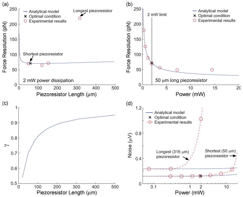
Force resolution of an optimal piezoresistive cantilever (Table III) with (a) various piezoresistor lengths and (b) various power dissipations. The optimization technique generated optimal cantilever designs while satisfying the bias voltage (< 2 V) and power dissipation (< 2 mW) constraints. (c) Geometry factor from finite-element method simulation with various piezoresistor lengths. The optimal piezoresistor length shifts from 57 to 120 μm because geometric factor dramatically decreases in short length as the length decreases. We used the same implantation dose in the piezoresistor and interconnects for all devices, but it is preferable to reduce the resistivity of the interconnects to improve the geometry factor. (d) Noise of both short and long piezoresistors (50 and 316 μm) with various power dissipations. Noise deviates from the analytical model, particularly when the piezoresistor is long or the power dissipation is high, and it affects force resolution.
The analytical model closely predicts the experimental force resolution. In Figs. 10 and 11(a) and (b), the experimental results are in good agreement with the analytical model for most cantilevers with various design and process parameters. The experimental sensitivity of all the cantilevers is slightly higher than the analytical model predicts, partly due to the cantilever air trench [Fig. 2(c)] which induces more stress in the piezoresistor for a given force, as reported previously [26], [27]. The experimental noise is also slightly higher than the analytical model because the overall resistance of the device is greater than the piezoresistor due to the interconnects and contact pads. The increased sensitivity and noise slightly offset each other to yield similar resolution as the analytical model.
However, the experimental data deviates from the analytical model, particularly when the dopant dose is low, the diffusion length is short (Fig. 10), the piezoresistor is long [Fig. 11(a)], or the power dissipation is high [Fig. 11(b)]. The force resolution of low-dose cantilevers (2 · 1014 cm−2 in Fig. 10) is worse than expected, because low-dose cantilevers have greater noise and drift due to large temperature coefficients both of resistivity and of piezoresistivity [24]. In Fig. 11(d), noise deviates from the analytical model, particularly when the piezoresistor is long or the power dissipation is high, and it affects force resolution of long piezoresistor [Fig. 11(a)] with high power dissipation [Fig. 11(b)].
Low-frequency (< 10 Hz) noise makes the force resolution deviate from the analytical model. Fig. 12(a) shows the noise of a cantilever operating at 1.2 mW. The experimental 1/f noise and Johnson noise (solid lines) agree with the analytical model (dash lines). However, the low-frequency noise of the cantilevers deviates from the analytical model as the power dissipation increases [Fig. 12(b) and (c)]. We found that the 1/fn noise below 10 Hz depends on the cantilever thickness and is a larger problem for thinner cantilevers. A piezoresistor test structure with no cantilever does not have the 1/fn noise even for high power dissipation. The problem becomes more severe as piezoresistor length increases [Fig. 11(d)]. These results suggest that the noise is related to the thermal resistance of the cantilever and that the noise increases with the cantilever temperature. The noise could be the result of temperature fluctuations or thermomechanical coupling due to unstable convection around the cantilever, leading to temperature fluctuations which are electrically coupled via a change in piezoresistivity with temperature [4]. This high-order 1/fn noise introduces another noise term which is under investigation; however, the analytical model presented here is useful and accurate for the design of cantilevers with low power dissipation. We are currently investigating the mechanisms underlying the increase in noise with larger power dissipation.
Fig. 12.
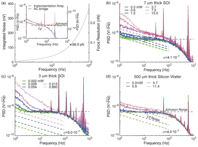
Noise spectra of sample piezoresistive cantilevers. (a) Optimal cantilever (Table III) operating at 2-V bias and 1.2 mW has 1/f noise (from ac bridge circuit) and Johnson noise (from instrumentation amplifier circuit). At 1–1000-Hz frequency, it has 88.9-pN force resolution. The (solid lines) experimental 1/f noise and Johnson noise agree with (dash lines) the analytical model. Low-frequency noise of (b) 7-μm- and (c) 3-μm-thick cantilevers and (d) the piezoresistor test structure fabricated without the cantilever with varying power dissipation. When the power dissipation increases or cantilevers are thin, the low-frequency noise, 1/fn noise, of the cantilevers deviates from the analytical model and leads to worse resolution.
VI. Conclusion
We have presented an analytical model for piezoresistive cantilever design and an optimization approach using TSUPREM4 process simulation for ion-implanted piezoresistors. We validated the approach by fabricating optimized cantilevers and characterizing their performance. The analytical model accurately predicted the force resolution of the devices, and the optimization technique generated optimal cantilever designs. Optimized performance is obtained by balancing Johnson noise, 1/f noise, and sensitivity while satisfying design constraints such as power dissipation. We introduced a characteristic number which indicates if cantilever performance is Johnson noise or 1/f noise dominated, and determines the optimal piezoresistor length. For Johnson-noise-dominated cantilevers, which include the devices we fabricated, the optimal force resolution depends on an interplay between the efficiency factor, maximum power dissipation, and maximum power bias voltage. Prior work on piezoresistive cantilever design has been limited to epitaxial piezoresistors, which we have extended to ion implantation and arbitrary dopant profiles in this paper.
Acknowledgments
This work was performed in part at the Stanford Nano-fabrication Facility (a member of the National Nanotechnology Infrastructure Network) which is supported by the National Science Foundation under Grant 9731293, its laboratory members, and the industrial members of the Stanford Center for Integrated Systems. The authors would like to thank the staff of the Stanford Nanofabrication Facility for the help with the fabrication. The authors are grateful to N. Harjee and J. R. Mallon, Jr., for the helpful discussions.
This work was supported in part by the National Science Foundation (NSF) under CAREER Award ECS-0449400 and Grant CTS-0428889, in part by the Center of Integrated Nanomechanical Systems under the NSF National Science and Engineering Center Grant ECS-0425914, in part by Nanoscale Exploratory Research under Grant ECCS-0708031, and in part by the National Institutes of Health under Grant R01 EB006745-01A1. The work of S.-J. Park was supported by a Samsung Fellowship. The work of J. C. Doll was supported in part by a National Defense Science and Engineering Graduate Fellowship and in part by an NSF Graduate Fellowship. Subject Editor K. E. Petersen.
Biographies

Sung-Jin Park (S'05–M'09) received the B.S. and M.S. degrees in mechanical engineering from Seoul National University, Seoul, Korea, in 1999 and 2003, respectively, and the Ph.D. degree from Stanford University, Stanford, CA, in 2009. During his Ph.D. studies, he developed a microelectromechanical-system-based tool, namely, a force clamp that uses appropriately scaled piezoresistive cantilevers and piezoelectric actuators with programmable real-time controllers to study mechanisms of mechanotransduction.
He is currently working with Prof. B. L. Pruitt as a Postdoctoral Researcher at Stanford University. His research interests include micro-/nanofabrication, device characterization and optimization, and system integration for biological measurements.

Joseph C. Doll (S'09) received the B.S. degree in mechanical engineering from the University of California, Berkeley, in 2006, and the M.S. degree from Stanford University, Stanford, CA, in 2009, where he is currently working toward the Ph.D. degree in mechanical engineering, focusing on the development of high-bandwidth force sensors and actuators to study the molecular basis of mechanotransduction in neurons.
Mr. Doll is the recipient of the award for best abstract at Microtechnologies in Medicine and Biology 2009.

Ali J. Rastegar (M'98) received the B.S. and M.S. degrees in electrical engineering from the Worcester Polytechnic Institute, Worcester, MA, in 1982 and 1984, respectively. He is currently working toward the Ph.D. degree in the Stanford Microsystems Laboratory, Stanford University, Stanford, CA.
He was an Integrated Circuit Design Engineer with Analog Devices, where he developed several high-speed state-of-the-art analog-to-digital converters. In 1992, he founded MCA Technologies, which was purchased by Maxim Integrated Products in 1997. In 2001, he became fascinated with the information storage capabilities of living cells. He has designed more than 54 integrated circuits and is the holder of eight issued U.S. patents.

Beth L. Pruitt (S'99–M'02) received the B.S. degree in mechanical engineering from the Massachusetts Institute of Technology, Cambridge, in 1991, and the M.S. degree in manufacturing systems engineering and the Ph.D. degree in mechanical engineering from Stanford University, Stanford, CA, in 1992 and 2002, respectively, supported by both the Hertz Foundation Fellowship and the Stanford Future Professors of Manufacturing Fellowship.
She was an Officer in the U.S. Navy with tours as an Engineering Project Manager at Naval Reactors, Washington, DC, and as an Engineering Instructor at the U.S. Naval Academy. She joined the mechanical engineering faculty at Stanford University in 2003. Her research interests include microelectromechanical systems, particularly metrologies for material characterization and biological measurements, and manufacturing and design for packaging, systems integration, and biomedical devices.
Dr. Pruitt is a Certified Professional Engineer. She is the recipient of the National Science Foundation CAREER Award and the Defense Advanced Research Projects Agency Young Faculty Award.
References
- 1.Barlian AA, Park WT, Mallon J, Rastegar AJ, Pruitt BL. Semiconductor piezoresistance for microsystems. Proc IEEE. 2009 Mar;97(3):513–552. doi: 10.1109/JPROC.2009.2013612. [DOI] [PMC free article] [PubMed] [Google Scholar]
- 2.Tortonese M, Barrett R, Quate C. Atomic resolution with an atomic force microscope using piezoresistive detection. Appl Phys Lett. 1993 Feb;62(8):834–836. [Google Scholar]
- 3.Mallon JR, Rastegar AJ, Barlian AA, Meyer MT, Fung TH, Pruitt BL. Low 1/f noise, full bridge, microcantilever with longitudinal and transverse piezoresistors. Appl Phys Lett. 2008 Jan;92(3):033 508. [Google Scholar]
- 4.Hansen O, Boisen A. Noise in piezoresistive atomic force microscopy. Nanotechnology. 1999;10(1):51–60. [Google Scholar]
- 5.Harley J, Kenny T. 1/f noise considerations for the design and process optimization of piezoresistive cantilevers. J Microelectromech Syst. 2000 Jun;9(2):226–235. [Google Scholar]
- 6.Yu X, Thaysen J, Hansen O, Boisen A. Optimization of sensitivity and noise in piezoresistive cantilevers. J Appl Phys. 2002 Nov;92(10):6296–6301. [Google Scholar]
- 7.Yang M, Zhang X, Vafai K, Ozkan CS. High sensitivity piezoresistive cantilever design and optimization for analyte-receptor binding. J Micromech Microeng. 2003 Nov;13(6):864–872. [Google Scholar]
- 8.Wang ZY, Yue RF, Zhang RX, Liu LT. Design and optimization of laminated piezoresistive microcantilever sensors. Sens Actuators A, Phys. 2005 May;120(2):325–336. [Google Scholar]
- 9.Harley JA, Kenny TW. High-sensitivity piezoresistive cantilevers under 1000 angstrom thick. Appl Phys Lett. 1999 Jul;75(2):289–291. [Google Scholar]
- 10.Park SJ, Doll J, Pruitt BL. Piezoresistive cantilever performance—Part I: Analytical model for sensitivity. J Microelectromech Syst. 2009 doi: 10.1109/JMEMS.2009.2036581. [DOI] [PMC free article] [PubMed] [Google Scholar]
- 11.Park SJ, Rastegar AJ, Mallon JR, Barlian AA, Fung TH, Pruitt BL. Ion implanted piezoresistive cantilever design and performance. Proc Solid State Sens., Actuators, Microsyst Workshop; Hilton Head, SC. Jun, 2008. pp. 98–101. [Google Scholar]
- 12.Pruitt B, Kenny T. Piezoresistive cantilevers and measurement system for characterizing low force electrical contacts. Sens Actuators A, Phys. 2003 Mar;104(1):68–77. [Google Scholar]
- 13.Barlian A, Park SJ, Mukundan V, Pruitt B. Design and characterization of microfabricated piezoresistive floating element-based shear stress sensors. Sens Actuators A, Phys. 2007 Feb;134(1):77–87. [Google Scholar]
- 14.Park SJ, Goodman MB, Pruitt BL. Analysis of nematode mechanics by piezoresistive displacement clamp. Proc Nat Acad Sci USA. 2007 Oct;104(44):17376–17381. doi: 10.1073/pnas.0702138104. [DOI] [PMC free article] [PubMed] [Google Scholar]
- 15.Muller RS, Kamins TI. Device Electronics for Integrated Circuits. New York: Wiley; 2003. [Google Scholar]
- 16.Richter J, Pedersen J, Brandbyge M, Thomsen E, Hansen O. Piezoresistance in p-type silicon revisited. J Appl Phys. 2008 Jul;104(2):023 715. [Google Scholar]
- 17.Runyan WR, Bean KE. Semiconductor Integrated Circuit Processing Technology Reading. MA: Addison-Wesley; 1990. [Google Scholar]
- 18.Vandamme LKJ, Hooge FN. What do we certainly know about 1/f noise in MOSTs? IEEE Trans Electron Devices. 2008 Nov;55(11):3070–3085. [Google Scholar]
- 19.Crandall SH, Dahl NC, Lardner TJ. Introduction to the Mechanics of Solids. New York: McGraw-Hill; 1978. [Google Scholar]
- 20.Young WC. Roark's Formulas for Stress and Strain. New York: McGraw-Hill; 1989. [Google Scholar]
- 21.Belendez T, Neipp C, Belendez A. Large and small deflections of a cantilever beam. Eur J Phys. 2002;23:371–379. [Google Scholar]
- 22.Matsuda K, Suzuki K, Yamamura K, Kanda Y. Nonlinear piezoresistance effects in silicon. J Appl Phys. 1993 Feb;73(3):1838–1847. [Google Scholar]
- 23.Chen J, MacDonald N. Measuring the nonlinearity of silicon piezoresistance by tensile loading of a submicron diameter fiber using a microinstrument. Rev Sci Instrum. 2004 Jan;75(1):276–278. [Google Scholar]
- 24.Kurtz AD, Gravel C. Semiconductor transducers using transverse and shear piezoresistance. Proc 22nd Annu ISA Conf.; Chicago, IL. Sep, 1967. pp. P4-PHYMMID-67 1–P4-PHYMMID-67 20. [Google Scholar]
- 25.Gel M, Shimoyama I. Force sensing submicrometer thick cantilevers with ultra-thin piezoresistors by rapid thermal diffusion. J Micromech Microeng. 2004 Mar;14(3):423–428. [Google Scholar]
- 26.Kassegne S, Madou M, Whitten R, Zoval J, Mather E, Sarkar K, Hodko D, Maity S. Design issues in soi-based high-sensitivity piezoresistive cantilever devices. Proc SPIE Conf Smart Struct Mater; San Diego, CA. Mar, 2002. pp. 588–597. [Google Scholar]
- 27.Amarasinghe R, Dao D, Dau V, Tung B, Sugiyama S. Sensitivity enhancement of piezoresistive micro acceleration sensors with nanometer stress concentration regions on sensing elements. Proc 15th Int Conf Solid-State Sens., Actuators, Microsyst., Transducers; Denver, CO. Jun, 2009. pp. 1333–1336. [Google Scholar]


