Abstract
An accurate analytical model for the change in resistance of a piezoresistor is necessary for the design of silicon piezoresistive transducers. Ion implantation requires a high-temperature oxidation or annealing process to activate the dopant atoms, and this treatment results in a distorted dopant profile due to diffusion. Existing analytical models do not account for the concentration dependence of piezoresistance and are not accurate for nonuniform dopant profiles. We extend previous analytical work by introducing two nondimensional factors, namely, the efficiency and geometry factors. A practical benefit of this efficiency factor is that it separates the process parameters from the design parameters; thus, designers may address requirements for cantilever geometry and fabrication process independently. To facilitate the design process, we provide a lookup table for the efficiency factor over an extensive range of process conditions. The model was validated by comparing simulation results with the experimentally determined sensitivities of piezoresistive cantilevers. We performed 9200 TSUPREM4 simulations and fabricated 50 devices from six unique process flows; we systematically explored the design space relating process parameters and cantilever sensitivity. Our treatment focuses on piezoresistive cantilevers, but the analytical sensitivity model is extensible to other piezoresistive transducers such as membrane pressure sensors.
Index Terms: Analytical model, force sensor, piezoresistance, piezoresistive cantilever
I. INTRODUCTION
Piezoresistivity is a commonly used transduction mechanism for microelectromechanical systems [1] such as force sensors [2]–[7], pressure sensors [8]–[12], stress sensors [13]–[15], microphones [16], accelerometers [17], [18], temperature sensors [19], [20], and chemical sensors [21]–[23]. Piezoresistive sensors have several desirable characteristics such as straightforward fabrication, simple signal-conditioning circuitry, relatively small size, and large dynamic range. Although optical readout is a more widely used technique to measure cantilever deflection, piezoresistive cantilevers are ideal for measurements where optical access is not possible or is inconvenient [7].
Many researchers have focused on improving the resolution of piezoresistive sensors [3]–[5], [8]–[11], [14]–[16], [18], [22], [23]. However, to simplify the analysis, previous work ignores the variation in dopant profile through the device thickness and approximates the dopant atoms as being concentrated at the surface [3], [5], [6], [8], [11]. However, this assumption leads to inaccurate device sensitivity predictions, particularly for thin devices where the diffusion length during processing is not negligible.
In this paper, we present an analytical model for piezoresistive cantilevers with nonuniform doping. To address the difference between theoretical estimates and experimental results of sensitivity, we define two nondimensional numbers: an efficiency factor β* and a geometry factor γ. The efficiency factor captures the reduction in sensitivity due to the dopant atoms being spread across the thickness, while the geometry factor addresses the reduction in sensitivity due to parasitic resistances.
The concept of an efficiency factor was first introduced by Tortonese et al. [2] and Harley and Kenny [4], but in this paper, we show, for the first time, how to directly relate an efficiency factor to sensitivity. Prior work assumed a constant piezoresistive coefficient throughout the device thickness; however, the piezoresistivity of silicon is a function of dopant concentration. Thus, the prior methods are only applicable to piezoresistors formed by epitaxy with negligible diffusion during processing and are not ideal for nonuniform profiles formed by ion implantation or diffusion.
We previously extended the concept of an efficiency factor to nonuniform dopant profiles [24]. In this paper, we validate the analytical model by fabricating and characterizing piezoresistive cantilevers and introduce the geometry factor which should also be considered in the design of real devices. In addition, we analyze the effect of design and process parameters on the efficiency factor and overall force sensitivity via simulation (9200 cases) with extensive experimental validation (50 devices from six unique process flows). Finally, we provide a lookup table to easily calculate the efficiency factor and sensitivity so that a process simulation tool is no longer necessary to predict the sensitivity. We present results for an ion-implanted piezoresistive cantilever, but the model is extensible to diffused piezoresistors [25] or 2-D stress distributions as found in membrane pressure sensors.
II. METHODS
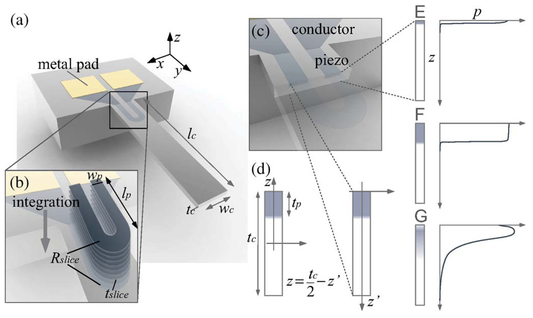
To validate the analytical sensitivity model, we designed and fabricated silicon piezoresistive cantilevers as described previously [26]. Briefly, the cantilevers were oriented in the 〈110〉 direction (E = 169 GPa) of a silicon-on-insulator wafer. P-type piezoresistors were formed by boron ion implantation, with doses ranging from 5 · 1015 to 5 · 1016 cm−2. We included designs of varying cantilever dimensions (length lc of 1.5–6 mm, width wc of 30–200 µm, and thickness tc of 7–50 µm) and varying piezoresistor dimensions (length lp of 200–350 µm and width wp of 10–20 µm) in Fig. 1. A wet oxidation at 1000–1150 °C (15–45 min) followed by an anneal in N2 at 1000–1150 °C (5–32 min) electrically activates the dopant and diffuses the dopant to varying extents.
Fig. 1.
Piezoresistive cantilever. (a) Geometry of cantilever. (b) Geometry of piezoresistor. (c) Strained region (piezoresistor) and unstrained regions (interconnects and contact pads) of the total resistance. (d) Coordinate change and dopant concentration profiles. (e) For maximum force sensitivity (all dopant atoms exist only at the surface). (f) For ideal epitaxial growth (dopant concentration is uniform within the junction depth). (g) For ion implantation, diffusion, or epitaxial growth with annealing process (dopant concentration has an approximately Gaussian distribution).
We attached the cantilevers to custom printed circuit boards (Imagineering Inc., Elk Grove Village, IL) with epoxy (Devcon, Glenview, IL) and wirebonded them with aluminum wire. The piezoresistor resistance change was transduced with a 1/4-active Wheatstone bridge and amplified with an instrumentation amplifier (Analog Devices AD8221 or Texas Instruments INA103, depending on the piezoresistor resistance) before data acquisition. Also, 1/4 of the bridge is an unstrained matched piezoresistor for temperature compensation.
We measured the spring constant, force sensitivity, and first-mode resonant frequency of each cantilever using a laser Doppler vibrometer (LDV) (Polytec OFV3001) [26]. The cantilever and printed circuit board were mounted on a piezoelectric shaker (Jodon, Ann Arbor, MI). The vibrometer laser was pointed at the tip of the cantilever to measure the velocity of the cantilever tip. We determined the resonant frequency f0 from the power spectral density of the LDV output while the shaker was driven with white noise; shaker drive signal and LDV measurement were accomplished with a vector signal analyzer (HP 89441A). We determined cantilever stiffness kc from the resonant frequency and dimensions of cantilever
| (1) |
which can also be written as
| (2) |
where ρc is the density of the cantilever. We calibrated the piezoresistor displacement sensitivity by shaking the cantilevers at their resonant frequency. Displacement voltage sensitivity is extracted from the tip displacement output of the vibrometer (SvibroVvibro/2πf0), and the voltage across the piezoresistors (Vpiezo) is measured from theWheatstone bridge
| (3) |
where Svibro and Vvibro are the velocity sensitivity and velocity voltage signal of the vibrometer, respectively.
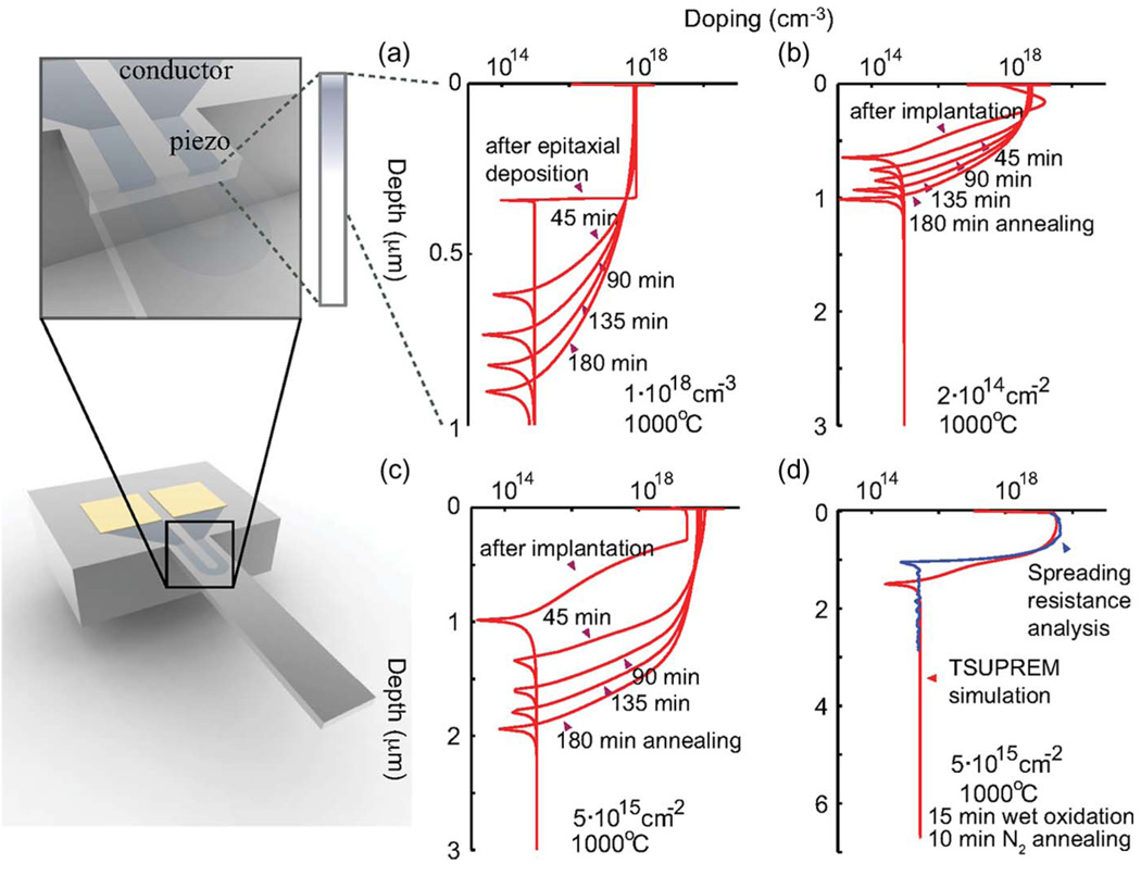
We simulated dopant profiles using TSUPREM4 (Synopsys, Mountain View, CA) (Fig. 2). To compute the efficiency factor and sensitivity of each cantilever, we used the fabrication process steps in Table I. We compared the simulation results with dopant profiles measured by spreading the resistance analysis (Solecon Laboratories, Reno, NV) of test structures (5 mm × 5 mm) fabricated during the piezoresistive cantilever process [Fig. 2(d)]. The geometry factor γ is calculated from finite-element analysis using COMSOL (COMSOL, Inc., Burlington, MA).
Fig. 2.
Dopant concentration profiles for the cantilever shown are simulated using TSUPREM4. The plots compare epitaxial and ion-implanted distributions. (a) Inert N2 anneal at 1000 °C for epitaxial deposition (dopant concentration: 1018 cm−3). (b) For low-dose ion implantation (dopant dose: 2 · 1014 cm−2). (c) For high-dose ion implantation (dopant dose: 5 · 1015 cm−2). (d) Comparison of dopant profiles between TSUPREM4 result and spreading resistance analysis data.
TABLE I.
Process Parameters of TSUPREM4 Simulation
| Process | Parameters |
|---|---|
| Screening 250 Å oxide growth |
wet O2 at 850°C for 17 min |
| Ion implant | Boron and BF2, 1014 to 5·1016 cm−2, 10 to 150 keV energy 7 °tilt |
| Strip screening oxide | all |
| Inert N2 anneal | Epitaxial: 700 to 1150°C Ion-implanted: 900 to 1150°C for 15 to 180 min (15 min step) |
III. ANALYTICAL MODEL FOR SENSITIVITY
A. Change in Resistance Due to Applied Stress
Piezoresistivity describes the change in the electrical resistance of a material due to the applied mechanical stress [27], [28]. To calculate the change in resistance due to the mechanical stress, we consider arbitrary profiles of both electrical resistance and mechanical stress, i.e., dopant concentration profile (p) and stress distribution (σ). Additionally, because resistivity ρ, carrier mobility μ, and piezoresistivity π are a function of dopant concentration, p, σ, ρ, μ, and π are defined locally. Therefore, it is necessary to average the change in resistance by integrating all local variables over the three dimensions.
In this paper, we derive the analytical solution for the sensitivity of a typical device with a U-shaped piezoresistor. We make four simplifying assumptions. First, we consider resistivity (ρl) only in the longitudinal direction of the piezoresistor. Current flow in a U-shaped piezoresistor can be assumed 1-D, because the piezoresistor length is much greater than its width. Second, we assume that the doping method is uniform across the wafer so that the dopant concentration varies only across the thickness of the piezoresistor. Third, lateral diffusion is negligible compared with diffusion in the thickness direction, because the width of the piezoresistor is much larger than the junction depth. Fourth, we neglect shear piezoresistivity, because longitudinal piezoresistors are insensitive to shear stress. Assuming plane stress [28], the change in resistance is a function of the longitudinal piezoresistance coefficient (πl), transverse piezoresistance coefficient (πt), normal stress parallel to the current (σl), and normal stress perpendicular to the current (σt)
| (4) |
or
| (5) |
where x, y, and z are oriented parallel to the width, length, and thickness of the device, respectively (Fig. 1).
We model the piezoresistor as a composite of many thin slices connected in parallel, where the resistivity and piezoresistance coefficient of each thin slice are constant. We calculate the change in resistance of each slice, then integrate the conductance, which is the inverse of resistance, to compute the overall resistance change (ΔR/R) due to the applied stress. The change in resistance (see Appendix for detailed calculations) is
| (6) |
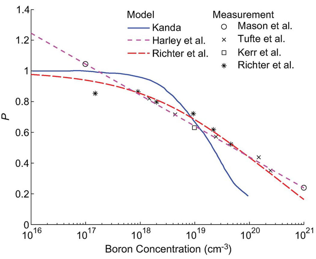
where σ̄l and σ̄t are the averages of longitudinal and transverse stresses in longitudinal direction, respectively . Pl and Pt are the longitudinal and transverse piezoresistance factors, obtained by dividing the local piezoresistance coefficient by the maximum obtainable, i.e., πl,max and πt,max. The piezoresistance factor P varies with temperature and dopant concentration, while πmax varies with piezoresistor orientation. Both Kanda’s theoretical model [28] based on Smith’s data [27] and Harley and Kenny’s empirical fit [4] based on experimental results [29]–[31] are available for the piezoresistance factor. A recent theoretical model by Richter et al. [32] analyzed the gap between Kanda’s model and Harley’s fit (Fig. 3). They achieved a good agreement between a theoretical model and experimental results if the full range of possible scattering mechanisms are considered, including acoustic phonon, nonpolar optical phonon, and ionized impurity scattering. Thus, we use the values obtained by Richter et al. for P and the maximum value for πmax, i.e., 72 · 10−11 Pa−1 in the [110] direction for silicon with a p-type dopant. In addition, carrier mobility is calculated as in [33]. Equation (6) is an analytical solution of the change in resistance for a piezoresistive device due to applied stress. If we know the dopant concentration profile p(z) and stress distribution σ(x, y, z) of the device, then we can calculate the change in resistance and, thus, the force and displacement sensitivity.
Fig. 3.
Piezoresistance factor as a function of boron concentration. We used the model presented by Richter et al. [32] to calculate β*. The models presented by Harley et al. [4] and Kanda [28] are shown for comparison and are accurate at low and high dopant concentrations, respectively.
B. Sensitivity of a Piezoresistive Cantilever
The stress distribution is readily calculated from Euler beam theory based upon the assumptions noted earlier. An external force F applied to the tip of the cantilever induces a uniaxial stress field
| (7) |
The sensitivity can be expressed in terms of force or displacement and in terms of change in resistance or voltage. We indicate the sensitivity (S) with subscripts (force F, displacementd, resistance Ω, and voltage V). From (6) and (7), the force sensitivity ((ΔR/R)/F) for an end-loaded beam is
| (8) |
This exact solution for force sensitivity captures both dopant and stress profile effects.
C. Geometry Factor γ
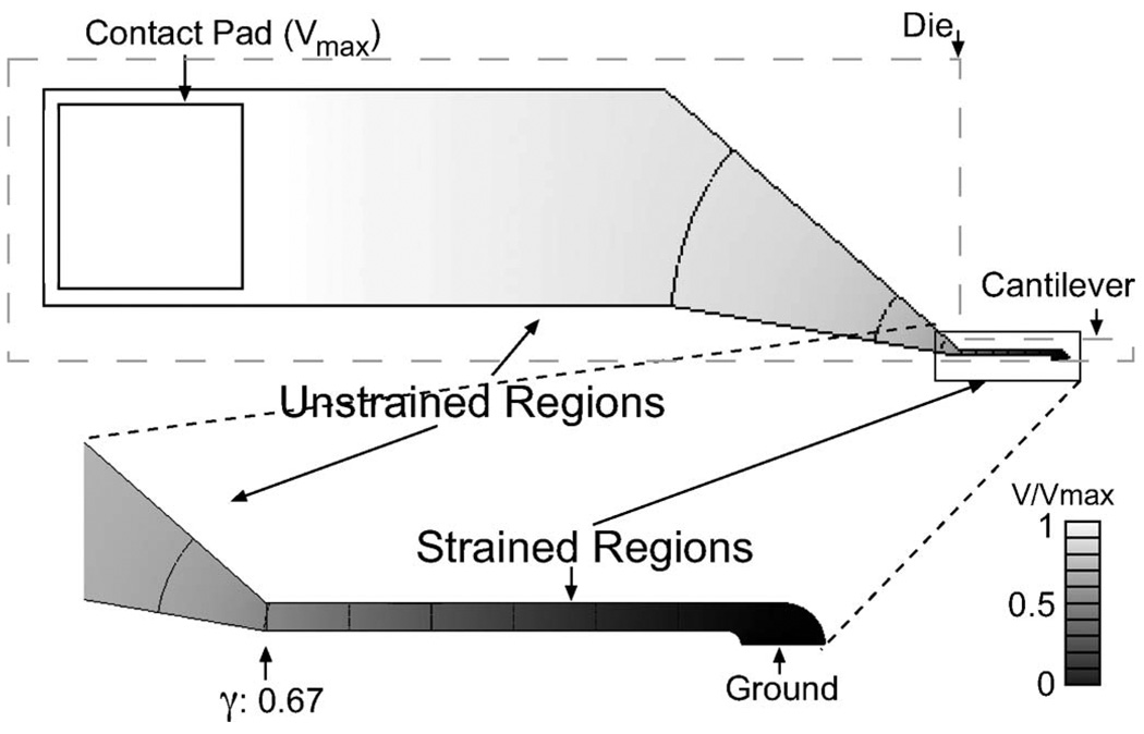
γ is a geometry factor defined as the ratio of the resistance of the strained region in the piezoresistor to the total resistance including unstrained regions, interconnects, and contact pads [Fig. 1(c)], which act to reduce force sensitivity (γ < 1). We can estimate the ratio of the resistance of the strained region to the total resistance by calculating the voltage distribution of a piezoresistor using finite-element analysis (Fig. 4).
Fig. 4.
Normalized voltage distribution of the typical cantilever which is simulated from finite-element analysis. The geometry factor γ addresses the reduction in sensitivity due to parasitic resistances of unstrained regions (0.33 of total resistance in the typical cantilever). Our typical cantilever has a U-shaped piezoresistor where both strained and unstrained regions have the same sheet resistance.
D. Efficiency Factor β*
We introduce an efficiency factor β* by dividing the force sensitivity for an arbitrary dopant concentration profile by the theoretical maximum force sensitivity. The theoretical maximum force sensitivity can be achieved if the dopant atoms exist only at the surface [z = t/2, Fig. 1(e)], and the dopant concentration is small enough to maintain the maximum piezoresistance factor (P = 1). If P = 1, then the force sensitivity becomes
| (9) |
The efficiency factor β* is defined as
| (10) |
Using this efficiency factor, the force sensitivity (8) for any arbitrary dopant profile may be expressed as
| (11) |
Considering a balanced 1/4-active Wheatstone bridge configuration ((Vout/Vbridge) ≈ (ΔR/4R)), voltage force sensitivity is
| (12) |
where Vbridge is the Wheatstone bridge bias voltage. From the force sensitivity (12) and spring constant kc (1), the displacement sensitivity is
| (13) |
In summary, we can calculate the force and displacement sensitivities [(12) and (13)] from the lateral cantilever dimensions (lc and wc), piezoresistor length (lp), and β*, which is a function of dopant profile and cantilever thickness (tc).
IV. EFFECT OF FABRICATION PROCESSES ON β*
β* describes how the dopant profile affects the sensitivity of the device. If dopants are close to the surface and the dopant concentration is low enough to maintain a high piezoresistance factor across the resistor, then β* is close to one. If the dopants are uniformly distributed through the thickness of the cantilever or the dopant concentration is very high, then β* approaches zero. β* is a function of only cantilever thickness and process parameters; therefore, devices from the same wafer and process have a single β* independent of cantilever length and width. The practical significance of this is that we can separate the process parameters from the design parameters, making it possible to design the cantilever geometry and fabrication process separately. Additionally, β* can be used for other piezoresistive devices besides cantilevers: The β* of an arbitrary device is the same as the β* of a piezoresistive cantilever (10) if σ in the device is linearly proportional to z in (6).
A. β* for Ideal Epitaxial Growth
In an ideal epitaxial piezoresistor [Fig. 1(f)] where dopant atom diffusion is negligible, the dopant concentration and the piezoresistance factor P are constant within the junction depth tp. Thus, the efficiency factor of an ideal epitaxial cantilever is
| (14) |
B. β* for Nonuniform Doping Profiles
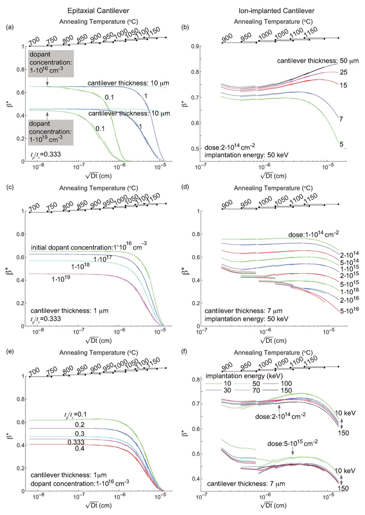
Diffusion of dopant atoms during high-temperature processes leads to a nonuniform dopant profile. The electrically active dopant concentration profile can be simulated with TSUPREM4 [Fig. 2(a)–(c)] or experimentally measured using spreading resistance analysis [Fig. 2(d)]. In Fig. 5, we calculated β* for epitaxial (A, C, and E) and ion-implanted (B, D, and F) cantilevers in various conditions such as different cantilever thickness (A and B), dopant concentration (C), implantation dose (D), epitaxial layer thickness (E), and implantation energy (F). To investigate how diffusion affects β* with various process conditions, β* in Fig. 5 was also calculated with various annealing conditions (temperature T and time t) and was plotted in terms of diffusion length . The diffusion coefficient is defined as D = Dioexp(−Eia/kBT), where for boron Dio = 0.037 cm2/s and Eia = 3.46 eV [34]. Each line corresponds to each annealing temperature plot with various times (15–180 min).
Fig. 5.
β* of epitaxial (a, c, and e) and ion-implanted (b, d, and f) cantilevers with various cantilever thicknesses (a and b), dopant concentration (c), implantation dose (d), epitaxial layer thickness (e), and implantation energy (f). Lines are discontinuous because the solid solubility limit depends upon the maximum processing temperature.
1) Effect of Cantilever Thickness on β*
Epitaxial piezoresistors can be approximated with (14) until the diffusion length is comparable to the cantilever thickness [Fig. 5(a)]. Similarly, ion-implanted piezoresistors have constant β* values until the diffusion length becomes significant [Fig. 5(b)]. The transition point depends on cantilever thickness; β* decreases in the case of thin cantilevers (5 and 7 µm), while β* increases with diffusion length in the case of thick cantilevers (15, 25, and 50 µm). The trend of β* with diffusion length depends upon two competing mechanisms: the depth effect and the piezoresistance factor effect. During diffusion, dopant atoms move from the top surface of the cantilever toward the neutral axis. Bending stress decreases linearly with depth; therefore, β* decreases with diffusion length due to the depth effect. However, the piezoresistance factor is inversely proportional to dopant concentration; therefore, diffusion simultaneously acts to increase β* by the piezoresistive factor effect. These two effects compete to determine the trend of β* with diffusion length. In relatively thin cantilevers, [Fig. 5(a) and (b)], the piezoresistance factor effect is negligible, and the depth effect dominates. However, for relatively thick cantilevers [15, 25, and 50 µm, Fig. 5(b)], the piezoresistance factor effect dominates until the junction depth is comparable to the half-thickness of the cantilever.
2) Effect of Concentration and Dose on β*
For epitaxial cantilevers of varied initial dopant concentration [Fig. 5(c)], β* decreases as the dopant concentration is increased. Ion-implanted cantilevers of varied doses [Fig. 5(d)] show a similar trend; β* of low-dose cantilevers is greater than that of cantilevers with a high implant dose. However, β* converges for high-dose minimal- processes because the effects of dopant activation and solid solubility limit become substantial. β* diverges with increasing diffusion length as dopant atoms are activated and diffuse away. Note that lightly doped piezoresistors have large β* values, but can lead to large drift and electrical noise and may not yield optimal resolution.
3) Effect of Initial Junction Depth on β*
Junction depth is defined as the depth where the doping concentration of a piezoresistor drops to background concentration. In the case of epitaxial piezoresistors with varying initial thickness ratios (tp/tc) [Fig. 5(e)], β* is inversely proportional to the thickness ratio as expected. Ion-implanted cantilevers show a similar trend [Fig. 5(f)]; the formation of shallow piezoresistors by reducing implantation energy tends to improve β* for a given dose. However, there is an exception to this trend in the case of low-dose low-diffusion-length piezoresistors where β* is actually improved with implantation energy because of the piezoresistance factor effect.
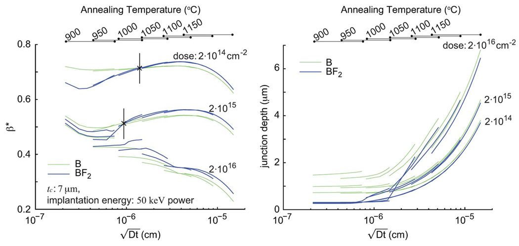
The effect of increasing ion mass for a fixed energy is similar to that of decreasing implantation energy [Fig. 5(f)] because the initial dopant depth is reduced. Bergaud et al. [35] demonstrated that ultrashallow piezoresistors can be fabricated by the implantation of more massive ions such as BF2. We calculated β* for cantilevers with boron and BF2 dopant atoms in Fig. 6. The competition between the depth and piezoresistance factor effects is evident in the results.
Fig. 6.
β* and junction depth of piezoresistor formed by B and BF2 ion implantation. Both low-power implantation and heavier ion implantation can yield better β* and force sensitivity. However, the low dose and short diffusion lengths needed to fabricate shallow piezoresistors with BF2 require a longer annealing process to achieve better β* and force sensitivity than elemental boron. The cross indicates diffusion lengths where β* of piezoresistors with BF2 is the same as β* of piezoresistors with B.
4) Effect of Annealing Atmosphere on β*
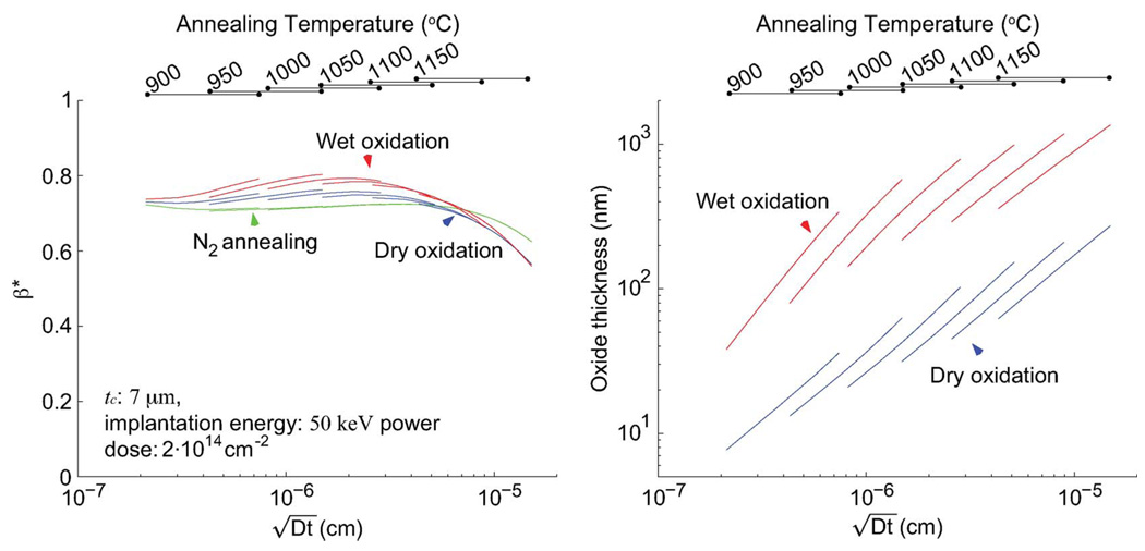
Next, we investigated the effect of the postimplantation annealing atmosphere on β* (Fig. 7). The trend of β* for dry and wet oxidation is similar to the trend for inert annealing. However, β* is greater for oxidizing environments because dopant segregation into the oxide acts to reduce the dopant concentration in the piezoresistor and increase β* by the piezoresistance factor effect. Oxide thickness is greater for wet growth than dry growth at any , and the thicker oxide leads to additional dopant segregation and oxidation-enhanced diffusion [36].
Fig. 7.
β* and oxide thickness of ion-implanted cantilever with different annealing methods. β* is greater for oxidizing environments because dopant segregation into the oxide acts to reduce the dopant concentration in the piezoresistor and increase β* by the piezoresistance factor effect. Note that β* versus of dry and wet oxidation is discontinuous for the different annealing temperature ranges, because of dopant segregation in the oxide.
C. Comparison With Other Analytical Models
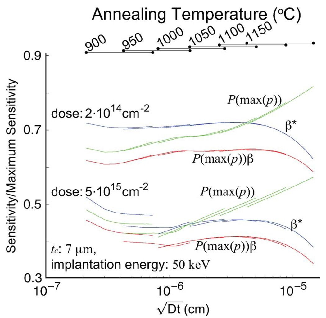
We compare the predicted force sensitivity from the idealized model [3], [5], [6], the Tortonese model [2], [4], [22], and our model in Fig. 8. The idealized model ignores the dopant profile and assumes that all of the dopant atoms exist at the top surface. This model is useful to estimate force sensitivity, but diverges from the exact solution for cantilevers with large diffusion lengths. Tortonese et al. [2] later considered the dopant profile by modifying the model to include an efficiency factor β, which accounts for the junction-depth effect only
| (15) |
Fig. 8.
Comparison with other analytical models. P(max(p)), P(max(p))β, and β* indicate the simplified model [5], the Tortonese model [2], [4], and our model, respectively. The disagreement in sensitivity between the three models depends on the fabrication process and cantilever thickness.
Comparing (10) and (15), the Tortonese model ignores the piezoresistance factor effect because the piezoresistance factors in the denominator and numerator cancel. The Tortonese model uses P(max(p)), taken as the piezoresistance factor at the maximum dopant concentration. As seen in Fig. 8, the Tortonese model underestimates force sensitivity.
D. β* Lookup Table
If we separate the dependence of β* from the thickness of the cantilever, then we can build a lookup table of β* for various processing conditions. Changing the coordinate system from the neutral axis to the surface of the cantilever [z′ = tc/2 − z, Fig. 1(d)], we write
| (16) |
If we assume that most dopants exist within the junction depth tp
| (17) |
where are defined as
| (18) |
| (19) |
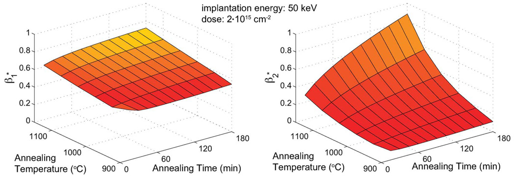
As defined, (piezoresistance factor effect) and (depth effect) depend only on processing parameters. is a conductivity weighted average of the piezoresistance factor. If dopant concentration is low, is high because the piezoresistance factor is high. is a stress- and depth-dependent term, i.e., how close are the dopant atoms to the maximum stress at the surface. If dopant atoms are located near the surface, is low, and then, β* depends on only. If the dopant atoms are distributed equally across the thickness of the cantilever, , and β* approaches zero. Finally, the thickness determines whether is dominant (17): β* depends more on for thick cantilevers where the piezoresistance factor effect is more important and on for thin cantilevers where the depth effect is more important.
We calculated based on TSUPREM4 simulations for inert (N2) annealing (Fig. 9) and provided a lookup table (Table II). The oxide layer is also required for passivation; therefore, we also calculated for a typical process with 1500-Å wet isolation oxide. One can estimate β* using the lookup table values and (17). For example, in the case of a 10-µm-thick cantilever with 2 · 1015 cm−2 implantation dose and a 30-min N2 anneal at 1000 °C, β* is 0.50 (0.53–0.13/5). To achieve a β* larger than zero in (17), cantilever thickness should be larger than two times ; therefore, in the case of the previous example, the cantilever thickness should be greater than 0.26 µm.
Fig. 9.
for boron-implanted piezoresistors (50-keV energy and 2 · 1015 cm−2 dose) with various inert (N2) annealing temperatures and times. (piezoresistance factor effect) and (depth effect) depend only on processing parameters.
TABLE II.
Lookup Table for (in micrometers) With Boron Implantation. The First Number Given Is for a Typical Process With 1500-Å Wet Isolation Oxide With N2 Annealing, While Values in Parentheses Are for Inert (N2) Annealing Alone. The Wet Isolation Oxide Was Grown at the Indicated Process Temperature for 66-, 15-, and 5-min Oxidation Time for 900 °C, 1000 °C, and 1100 °C, Respectively, and the Wafer Is Then Annealed at the Same Process Temperature for the Time Indicated in the Table. β* of Piezoresistive Device Is Calculated Using (17). For Example, β* of 10-µm-Thick Device With 2·1015 cm−2 Implantation Dose at 50 keV and a 30-min N2 Anneal At 1000 °C Is 0.53 From
| Implantation Dose (cm−2) |
Implantation Energy (keV) |
Annealing Temp (°C) |
Annealing Time (min) | ||||||||||||||||||||||||||||
|---|---|---|---|---|---|---|---|---|---|---|---|---|---|---|---|---|---|---|---|---|---|---|---|---|---|---|---|---|---|---|---|
| 15 | 30 | 45 | 60 | 75 | 90 | 105 | 120 | ||||||||||||||||||||||||
| 900 | .84(.74) | .19(.09) | .84(.73) | .19(.09) | .84(.72) | .19(.09) | .84(.72) | .19(.09) | .84(.72) | .19(.09) | .84(.73) | .19(.09) | .84(.73) | .19(.09) | .84(.73) | .20(.09) | |||||||||||||||
| 30 | 1000 | .86(.72) | .26(.09) | .86(.74) | .26(.11) | .86(.74) | .27(.12) | .86(.75) | .27(.13) | .86(.75) | .27(.14) | .87(.76) | .28(.15) | .87(.76) | .28(.16) | .87(.77) | .29(.16) | ||||||||||||||
| 1100 | .88(.77) | .43(.17) | .88(.79) | .45(.22) | .89(.80) | .47(.27) | .89(.81) | .49(.31) | .89(.82) | .51(.34) | .89(.82) | .53(.37) | .89(.83) | .55(.40) | .89(.83) | .57(.43) | |||||||||||||||
| 900 | .82(.76) | .22(.14) | .82(.75) | .22(.13) | .82(.75) | .22(.13) | .82(.74) | .22(.13) | .82(.75) | .22(.13) | .82(.75) | .22(.14) | .82(.75) | .22(.14) | .82(.75) | .22(.14) | |||||||||||||||
| 2·1014 | 50 | 1000 | .84(.74) | .28(.13) | .85(.75) | .28(.14) | .85(.76) | .29(.15) | .85(.76) | .29(.16) | .85(.76) | .30(.17) | .85(.77) | .30(.17) | .85(.77) | .31(.18) | .85(.77) | .31(.19) | |||||||||||||
| 1100 | .87(.77) | .44(.19) | .87(.79) | .47(.24) | .87(.80) | .49(.28) | .88(.81) | .51(.32) | .88(.82) | .53(.35) | .88(.82) | .55(.38) | .88(.82) | .57(.41) | .88(.83) | .59(.44) | |||||||||||||||
| 900 | .81(.78) | .29(.23) | .81(.78) | .29(.23) | .81(.78) | .29(.23) | .81(.78) | .29(.23) | .82(.78) | .29(.23) | .82(.78) | .29(.23) | .82(.78) | .29(.23) | .82(.78) | .29(.23) | |||||||||||||||
| 100 | 1000 | .83(.77) | .34(.22) | .83(.77) | .34(.23) | .83(.78) | .35(.23) | .84(.78) | .35(.24) | .84(.78) | .36(.24) | .84(.79) | .36(.25) | .84(.79) | .36(.25) | .84(.79) | .37(.26) | ||||||||||||||
| 1100 | .86(.79) | .49(.26) | .86(.80) | .51(.30) | .86(.81) | .53(.34) | .86(.82) | .55(.37) | .87(.82) | .57(.40) | .87(.83) | .59(.43) | .87(.83) | .61(.45) | .87(.83) | .62(.48) | |||||||||||||||
| 900 | .69(.56) | .17(.08) | .69(.53) | .17(.07) | .69(.52) | .18(.07) | .69(.52) | .18(.08) | .69(.52) | .18(.08) | .69(.52) | .18(.08) | .69(.52) | .18(.09) | .69(.53) | .18(.09) | |||||||||||||||
| 30 | 1000 | .70(.53) | .25(.10) | .70(.55) | .26(.12) | .70(.57) | .27(.15) | .70(.58) | .27(.16) | .70(.58) | .28(.18) | .71(.59) | .28(.19) | .71(.60) | .29(.20) | .71(.60) | .29(.21) | ||||||||||||||
| 1100 | .73(.59) | .45(.19) | .74(.62) | .48(.25) | .74(.63) | .51(.30) | .75(.64) | .53(.34) | .75(.65) | .55(.38) | .75(.66) | .57(.41) | .75(.67) | .59(.44) | .76(.67) | .61(.47) | |||||||||||||||
| 900 | .64(.57) | .18(.11) | .64(.53) | .18(.10) | .64(.52) | .18(.10) | .65(.52) | .18(.10) | .65(.52) | .18(.10) | .65(.52) | .19(.10) | .65(.52) | .19(.10) | .65(.53) | .19(.10) | |||||||||||||||
| 2·1015 | 50 | 1000 | .68(.53) | .26(.11) | .68(.55) | .27(.13) | .69(.57) | .27(.15) | .69(.57) | .28(.17) | .69(.58) | .29(.18) | .69(.59) | .29(.20) | .69(.59) | .30(.21) | .69(.60) | .30(.22) | |||||||||||||
| 1100 | .72(.59) | .44(.20) | .72(.61) | .46(.26) | .72(.63) | .49(.31) | .73(.64) | .51(.35) | .73(.65) | .53(.38) | .73(.66) | .55(.42) | .74(.66) | .57(.45) | .74(.67) | .59(.47) | |||||||||||||||
| 900 | .63(.60) | .24(.19) | .63(.57) | .24(.18) | .63(.56) | .24(.17) | .63(.56) | .24(.17) | .63(.56) | .24(.17) | .63(.56) | .24(.18) | .63(.56) | .24(.18) | .63(.56) | .24(.18) | |||||||||||||||
| 100 | 1000 | .67(.57) | .31(.17) | .67(.58) | .32(.18) | .67(.59) | .32(.19) | .68(.59) | .33(.21) | .68(.60) | .33(.22) | .68(.60) | .34(.23) | .68(.60) | .34(.24) | .68(.61) | .35(.25) | ||||||||||||||
| 1100 | .70(.60) | .46(.23) | .71(.62) | .49(.29) | .71(.63) | .51(.33) | .71(.64) | .54(.37) | .72(.65) | .56(.40) | .72(.66) | .58(.43) | .72(.66) | .60(.46) | .72(.67) | .62(.49) | |||||||||||||||
| 900 | .55(.55) | .14(.11) | .55(.52) | .14(.10) | .55(.51) | .15(.10) | .55(.51) | .15(.11) | .55(.51) | .15(.11) | .55(.51) | .15(.11) | .54(.51) | .16(.12) | .54(.51) | .16(.12) | |||||||||||||||
| 30 | 1000 | .49(.43) | .23(.11) | .49(.44) | .25(.14) | .49(.45) | .27(.17) | .49(.45) | .28(.19) | .49(.45) | .30(.21) | .50(.45) | .31(.23) | .50(.45) | .33(.25) | .50(.45) | .34(.27) | ||||||||||||||
| 1100 | .51(.41) | .47(.22) | .51(.42) | .51(.32) | .52(.45) | .55(.40) | .52(.46) | .58(.46) | .53(.47) | .62(.52) | .53(.48) | .64(.56) | .54(.48) | .67(.60) | .54(.49) | .70(.64) | |||||||||||||||
| 900 | .53(.54) | .15(.13) | .53(.51) | .15(.12) | .53(.50) | .15(.12) | .53(.50) | .15(.12) | .53(.50) | .15(.13) | .53(.50) | .15(.13) | .53(.50) | .16(.13) | .52(.50) | .16(.14) | |||||||||||||||
| 2·1016 | 50 | 1000 | .48(.42) | .23(.12) | .48(.43) | .25(.15) | .48(.44) | .27(.18) | .48(.44) | .29(.20) | .48(.44) | .31(.22) | .48(.44) | .32(.24) | .48(.45) | .34(.26) | .48(.45) | .35(.27) | |||||||||||||
| 1100 | .50(.41) | .48(.23) | .51(.42) | .52(.33) | .51(.44) | .56(.41) | .52(.46) | .59(.47) | .52(.47) | .63(.52) | .52(.47) | .66(.57) | .53(.48) | .68(.61) | .53(.49) | .71(.65) | |||||||||||||||
| 900 | .52(.55) | .21(.20) | .52(.51) | .21(.19) | .52(.50) | .21(.18) | .52(.50) | .21(.18) | .52(.50) | .21(.18) | .52(.50) | .21(.18) | .52(.50) | .21(.19) | .52(.50) | .21(.19) | |||||||||||||||
| 100 | 1000 | .47(.42) | .24(.15) | .47(.42) | .26(.17) | .47(.43) | .28(.20) | .47(.43) | .29(.22) | .47(.43) | .31(.24) | .47(.43) | .33(.26) | .48(.44) | .34(.27) | .48(.44) | .36(.29) | ||||||||||||||
| 1100 | .50(.40) | .50(.24) | .50(.43) | .54(.35) | .51(.45) | .57(.43) | .51(.46) | .61(.49) | .52(.47) | .64(.54) | .52(.48) | .67(.58) | .52(.48) | .70(.62) | .53(.49) | .72(.66) | |||||||||||||||
V. EXPERIMENTAL VALIDATION
We validated the analytical model by comparing it with numerical simulation and experimental measurements of ion-implanted piezoresistive cantilevers. Based on three different piezoresistance factors (the theoretical values of Richter et al. [32], Harley and Kenny’s empirical model [4], and Kanda’s theoretical values [28]), we calculated β* from displacement sensitivity (13) and resonant frequency equations measured by LDV
| (20) |
where ρs is the density of the cantilever and γ is calculated using finite-element analysis.
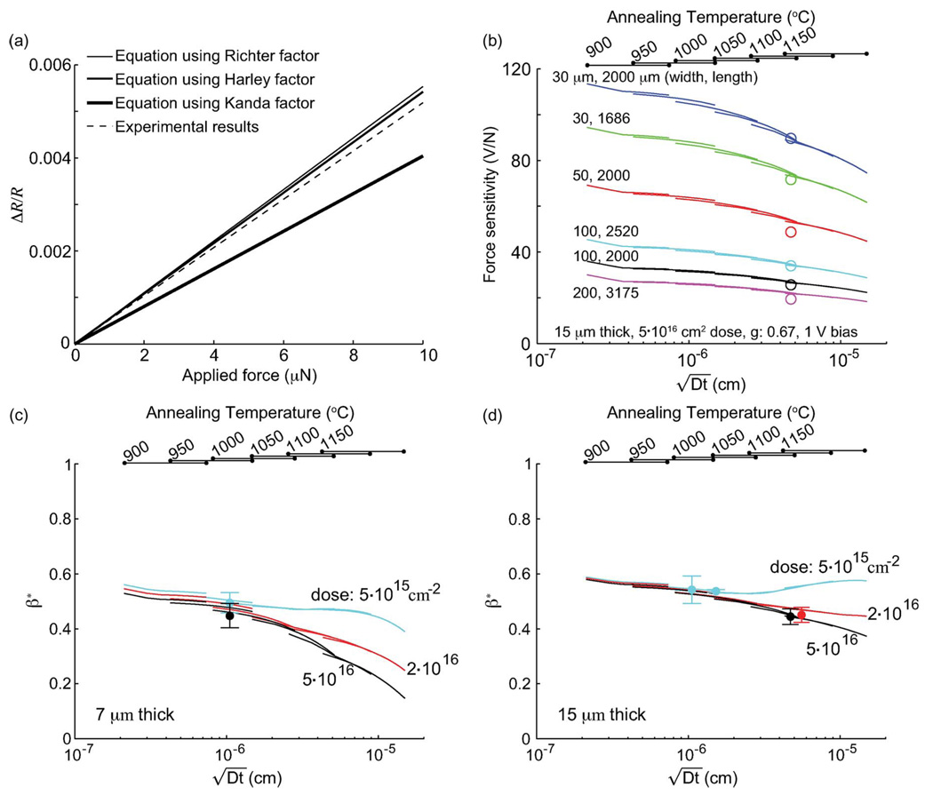
The predicted force sensitivity and β* are in good agreement with the experimental results (Fig. 10). Fig. 10(a) shows the change in resistance based on the analytical model and experimental results when a point force is applied at the tip. The fits from Harley’s and Richter’s data are more accurate than Kanda’s at the high dopant concentrations (> 5 · 1019 cm−3) applicable to our devices. Fig. 10(b)–(d) shows the force sensitivity and β* as a function of diffusion length for cantilevers of varying ion implantation doses and cantilever dimensions. Most of the results are within 5% of the model; however, there are a few points where the deviation from the analytical model is up to 20%. Errors could result from the lateral spreading of dopants due to diffusion, fabrication and experimental uncertainty, or operating temperature fluctuations with resistance heating. The contribution of electrical current due to the lateral spreading of dopants is up to 6% in our case (wp/tp ~ 5). The uncertainty of measured β* in (20) is 7.4% from an uncertainty analysis [37] including variation in lp/lc, γ, the Young’s modulus, density, and the piezoresistance coefficient possibly from the misalignment of the cantilevers from the [110] direction as well as the undercut of the clamped boundary during backside release. Measured β* values from thin cantilevers depart from the model more than thick cantilevers. We believe the cases with larger errors due to the thermal resistance of the cantilever and the decrease in piezoresistance with temperature [32].
Fig. 10.
Validation of the analytical model. (a) Comparison of analytical models for the piezoresistance factor as a function of dopant concentration and experimental results of changes in resistance of a typical piezoresistive cantilever (2000-µm-long 30-µm-wide 15-µm-thick cantilever with 350-µm-long by 10-µm-wide U-shaped piezoresistor having the dopant profile in Fig. 2(d)) based on piezoresistance factors of the theoretical values of Richter [32], Harley and Kenny’s empirical model [4], and Kanda’s theoretical values [28]. (b) Force sensitivity of piezoresistive cantilevers with various cantilever dimensions. (c and d) β* of 7- and 15- µm-thick piezoresistive cantilever. Each point of (b) indicates a sensitivity result of one device with different cantilever dimensions, and each point of (c and d) represents measured β* values of two to seven devices from different wafers fabricated with different process conditions. The (solid lines) analytical model is in good agreement with (circles) experimental results.
For typical 7-µm-thick cantilevers with 15-min wet oxidation and 10-min N2 annealing at 1000 °C, β* = 0.50 from TSUPREM4, β* = 0.46 from dopant profiles from spreading resistance analysis [Fig. 2(d)], and β* = 0.49 ± 0.04 (N = 5 devices and 1 wafer) from experimental sensitivity. Although TSUPREM4 predicts a greater junction depth than that measured with spreading resistance analysis, β* is dominated by the high-concentration regions where the agreement between the two is excellent. In addition, we found that β* for various cantilever geometries (1686–3175 µm long and 30–200 µm wide) from a single wafer have only 0.04 standard deviation. This repeatability demonstrates that all devices from a single wafer (with uniform device thickness) have the same β*, independent of cantilever geometry.
VI. CONCLUSION
We have presented an improved analytical model of piezoresistive cantilever sensitivity. In addition, we investigated the effect of cantilever design and process parameters (device thickness, implant dose, implant energy, dopant atom, and annealing atmosphere) on the efficiency factor and force sensitivity. We found that there are two competing effects: the depth effect and the piezoresistance factor effect, which determine the overall efficiency factor β*. Optimal conditions may be defined to maximize the efficiency factor and sensitivity when the two competing effects are balanced. We characterized numerous piezoresistive cantilevers over a range of process conditions and verified that the model agrees with simulation and experiment. By separating the wafer processing parameters from cantilever geometry, the design process is simplified, and process and geometry design are decoupled. Finally, we have also provided a lookup table for design guidance, so that other researchers can quickly and accurately predict sensitivity for piezoresistive devices.
ACKNOWLEDGMENT
This work was performed in part at the Stanford Nanofabrication Facility (a member of the National Nanotechnology Infrastructure Network) which is supported by the National Science Foundation under Grant 9731293, its laboratory members, and the industrial members of the Stanford Center for Integrated Systems. The authors would like to thank the staff of the Stanford Nanofabrication Facility for the help with the fabrication. The authors are grateful to N. Harjee and J. R. Mallon, Jr., for the helpful discussions.
This work was supported in part by the National Science Foundation (NSF) under CAREER Award ECS-0449400 and Grant CTS-0428889, in part by the Center of Integrated Nanomechanical Systems under the NSF National Science and Engineering Center Grant ECS-0425914, in part by Nanoscale Exploratory Research under Grant ECCS-0708031, and in part by the National Institutes of Health under Grant R01 EB006745-01A1. The work of S.-J. Park was supported by a Samsung Fellowship. The work of J. C. Doll was supported in part by a National Defense Science and Engineering Graduate Fellowship and in part by an NSF Graduate Fellowship. Subject Editor K. E. Petersen.
Biographies

Sung-Jin Park (S’05–M’09) received the B.S. and M.S. degrees in mechanical engineering from Seoul National University, Seoul, Korea, in 1999 and 2003, respectively, and the Ph.D. degree from Stanford University, Stanford, CA, in 2009. During his Ph.D. studies, he developed a microelectromechanical-system-based tool, namely, a force clamp that uses appropriately scaled piezoresistive cantilevers and piezoelectric actuators with programmable real-time controllers to study mechanisms of mechanotransduction.
He is currently working with Prof. B. L. Pruitt as a Postdoctoral Researcher at Stanford University. His research interests include micro-/nanofabrication, device characterization and optimization, and system integration for biological measurements.

Joseph C. Doll (S’09) received the B.S. degree in mechanical engineering from the University of California, Berkeley, in 2006, and the M.S. degree from Stanford University, Stanford, CA, in 2009, where he is currently working toward the Ph.D. degree in mechanical engineering, focusing on the development of high-bandwidth force sensors and actuators to study the molecular basis of mechanotransduction in neurons.
Mr. Doll is the recipient of the award for best abstract at Microtechnologies in Medicine and Biology 2009.

Beth L. Pruitt (S’99–M’02) received the B.S. degree in mechanical engineering from the Massachusetts Institute of Technology, Cambridge, in 1991, and the M.S. degree in manufacturing systems engineering and the Ph.D. degree in mechanical engineering from Stanford University, Stanford, CA, in 1992 and 2002, respectively, supported by both the Hertz Foundation Fellowship and the Stanford Future Professors of Manufacturing Fellowship.
She was an Officer in the U.S. Navy with tours as an Engineering Project Manager at Naval Reactors, Washington, DC, and as an Engineering Instructor at the U.S. Naval Academy. She joined the mechanical engineering faculty at Stanford University in 2003. Her research interests include microelectromechanical systems, particularly metrologies for material characterization and biological measurements, and manufacturing and design for packaging, systems integration, and biomedical devices.
Dr. Pruitt is a Certified Professional Engineer. She is the recipient of the National Science Foundation CAREER Award and the Defense Advanced Research Projects Agency Young Faculty Award.
APPENDIX
VII. CALCULATION OF TOTAL CHANGE IN RESISTANCE OF PIEZORESISTOR
Consider a thin slice of cantilever with tslice thickness. The total resistance of the slice is
| (21) |
Similarly, the change in resistance of a slice of the piezoresistor due to piezoresistivity is
| (22) |
Dividing (22) by (21), we calculate the ratio of resistance change
| (23) |
where σ̄l and σ̄t are the averages of longitudinal and transverse stresses in longitudinal direction, respectively .
We integrate the conductance change, which is the inverse of the resistance change of slices across the thickness of the cantilever to calculate the total change in the resistance of the piezoresistor. Since the slices of the piezoresistor are connected in parallel, we calculate conductance rather than resistance. Overall, conductance is
| (24) |
Since the change in resistance is the negative of the change in conductance (ΔR/R = −ΔG/G), the change in conductance is
| (25) |
| (26) |
Then, using (24) and (26), we can calculate the change in resistance
| (27) |
We introduce the longitudinal piezoresistance factor Pl = πl/πl,max and the transverse piezoresistance factor Pt = πt/πt,max, where πl,max and πt,max are the maximum longitudinal and transverse piezoresistivities as a function of direction at 300 K, respectively. Then, the change in resistance is
| (28) |
Footnotes
Color versions of one or more of the figures in this paper are available online at http://ieeexplore.ieee.org.
REFERENCES
- 1.Barlian AA, Park W-T, Mallon J, Rastegar AJ, Pruitt BL. Semiconductor piezoresistance for microsystems. Proc. IEEE. 2009 Mar;vol. 97(no. 3):513–552. doi: 10.1109/JPROC.2009.2013612. [DOI] [PMC free article] [PubMed] [Google Scholar]
- 2.Tortonese M, Barrett R, Quate C. Atomic resolution with an atomic force microscope using piezoresistive detection. Appl.Phys. Lett. 1993 Feb;vol. 62(no. 8):834–836. [Google Scholar]
- 3.Hansen O, Boisen A. Noise in piezoresistive atomic force microscopy. Nanotechnology. 1999 Mar;vol. 10(no. 1):51–60. [Google Scholar]
- 4.Harley J, Kenny T. 1/f noise considerations for the design and process optimization of piezoresistive cantilevers. J. Microelectromech. Syst. 2000 Jun;vol. 9(no. 2):226–235. [Google Scholar]
- 5.Yu X, Thaysen J, Hansen O, Boisen A. Optimization of sensitivity and noise in piezoresistive cantilevers. J. Appl. Phys. 2002 Nov;vol. 92(no. 10):6296–6301. [Google Scholar]
- 6.Duc TC, Creemer JF, Sarro PM. Piezoresistive cantilever beam for force sensing in two dimensions. IEEE Sensors J. 2007 Jan;vol. 7(no. 1):96–104. [Google Scholar]
- 7.Park S-J, Goodman MB, Pruitt BL. Analysis of nematode mechanics by piezoresistive displacement clamp. Proc. Nat. Acad. Sci. U.S.A. 2007 Oct;vol. 104(no. 44):17376–17381. doi: 10.1073/pnas.0702138104. [DOI] [PMC free article] [PubMed] [Google Scholar]
- 8.Kanda Y, Yasukawa A. Optimum design considerations for silicon piezoresistive pressure sensors. Sens. Actuators A, Phys. 1997 Jul;vol. 62(no. 1–3):539–542. [Google Scholar]
- 9.Merlos A, Santander J, Alvarez M, Campabadal F. Optimized technology for the fabrication of piezoresistive pressure sensors. J. Micromech. Microeng. 2000 Jun;vol. 10(no. 2):204–208. [Google Scholar]
- 10.Bae B, Flachsbart B, Park K, Shannon M. Design optimization of a piezoresistive pressure sensor considering the output signal-to-noise ratio. J. Micromech. Microeng. 2004 Dec;vol. 14(no. 12):1597–1607. [Google Scholar]
- 11.Pramanik C, Saha H, Gangopadhyay U. Design optimization of a high performance silicon MEMS piezoresistive pressure sensor for biomedical applications. J. Micromech. Microeng. 2006 Oct;vol. 16(no. 10):2060–2066. [Google Scholar]
- 12.Cho C-H, Jaeger RC, Suhling JC, Kang Y, Mian A. Characterization of the temperature dependence of the pressure coefficients of n- and p-type silicon using hydrostatic testing. IEEE Sensors J. 2008 Apr;vol. 8(no. 4):392–400. [Google Scholar]
- 13.Bartholomeyczik J, Brugger S, Ruther P, Paul O. Multidimensional CMOS in-plane stress sensor. IEEE Sensors J. 2005 Oct;vol. 5(no. 5):872–882. [Google Scholar]
- 14.Doelle M, Mager D, Ruther P, Paul O. Geometry optimization for planar piezoresistive stress sensors based on the pseudo-Hall effect. Sens. Actuators A, Phys. 2006 Mar;vol. 127(no. 2):261–269. [Google Scholar]
- 15.Li Y, Papila M, Nishida T, Cattafesta L, Sheplak M. Modeling and optimization of a side-implanted piezoresistive shear stress sensor; Proc. SPIE’s Int. Symp. Smart Struct. Mater; San Diego, CA: 2006. Feb, [Google Scholar]
- 16.Bhardwaj S, Sheplak M, Nishida T. S/N optimization and noise considerations for piezoresistive microphones; Proc 16th Int. Conf. Noise Phys. Syst. 1/f Fluctuations; Gainesville, FL: 2001. Oct, pp. 549–552. [Google Scholar]
- 17.Lee KI, Takao H, Sawada K, Ishida M. Low temperature dependence three-axis accelerometer for high temperature environments with temperature control of SOI piezoresistors. Sens. Actuators A, Phys. 2003 Mar;vol. 104(no. 1):53–60. [Google Scholar]
- 18.Wang Z, Xu Y. Design and optimization of an ultra-sensitive piezoresistive accelerometer for continuous respiratory sound monitoring. Sens. Lett. 2007 Jun;vol. 5(no. 2):450–458. [Google Scholar]
- 19.Lee J, King WP. Improved all-silicon microcantilever heaters with integrated piezoresistive sensing. J. Microelectromech. Syst. 2008 Apr;vol. 17(no. 2):432–445. [Google Scholar]
- 20.Lee J, Spadaccini CM, Mukerjee EV, King WP. Differential scanning calorimeter based on suspended membrane single crystal silicon microhotplate. J. Microelectromech. Syst. 2008 Dec;vol. 17(no. 6):1513–1525. [Google Scholar]
- 21.Hierlemann A, Lange D, Hagleitner C, Kerness N, Koll A, Brand O, Baltes H. Application-specific sensor systems based on CMOS chemical microsensors. Sens. Actuators B, Chem. 2000 Nov;vol. 70(no. 1–3):2–11. [Google Scholar]
- 22.Yang M, Zhang X, Vafai K, Ozkan CS. High sensitivity piezoresistive cantilever design and optimization for analyte-receptor binding. J. Micromech. Microeng. 2003 Nov;vol. 13(no. 6):864–872. [Google Scholar]
- 23.Loui A, Goericke FT, Ratto TV, Lee J, Hart BR, King WP. The effect of piezoresistive microcantilever geometry on cantilever sensitivity during surface stress chemical sensing. Sens. Actuators A, Phys. 2008 Oct;vol. 147(no. 2):516–521. [Google Scholar]
- 24.Park S-J, Rastegar AJ, Mallon JR, Barlian AA, Fung TH, Pruitt BL. Proc Solid State Sens., Actuators, Microsyst. Workshop. Hilton Head Island, SC: 2008. Jun, Ion implanted piezoresistive cantilever design and performance; pp. 98–101. [Google Scholar]
- 25.Doll JC, Park S-J, Pruitt BL. Design optimization of piezoresistive cantilevers for force sensing in air and water. J. Appl. Phys. 2009 Sep;vol. 106(no. 6):064310. doi: 10.1063/1.3224965. [DOI] [PMC free article] [PubMed] [Google Scholar]
- 26.Pruitt B, Kenny T. Piezoresistive cantilevers and measurement system for characterizing low force electrical contacts. Sens. Actuators A, Phys. 2003 Mar;vol. 104(no. 1):68–77. [Google Scholar]
- 27.Smith C. Piezoresistance effect in germanium and silicon. Phys. Rev. 1954 Apr;vol. 94(no. 1):42–49. [Google Scholar]
- 28.Kanda Y. Piezoresistance effect of silicon. Sens. Actuators A, Phys. 1991 Jul;vol. 28(no. 2):83–91. [Google Scholar]
- 29.Mason W, Forst J, Tornillo L. Recent developments in semiconductor strain transducers; Proc. Instrum. Soc. Amer. 15th Annu. Conf; 1962. pp. 110–120. [Google Scholar]
- 30.Tufte O, Stelzer E. Piezoresistive properties of silicon diffused layers. J. Appl. Phys. 1963 Feb;vol. 34(no. 2):313–318. [Google Scholar]
- 31.Kerr D, Milnes A. Piezoresistance of diffused layers in cubic semiconductors. J. Appl. Phys. 1963 Apr;vol. 34(no. 4):727–731. [Google Scholar]
- 32.Richter J, Pedersen J, Brandbyge M, Thomsen E, Hansen O. Piezoresistance in p-type silicon revisited. J. Appl. Phys. 2008 Jul;vol. 104(no. 2):023715. [Google Scholar]
- 33.Muller RS, Kamins TI. Device Electronics for Integrated Circuits. New York: Wiley; 2003. [Google Scholar]
- 34.Runyan WR, Bean KE. Semiconductor Integrated Circuit Processing Technology. Reading, MA: Addison-Wesley; 1990. [Google Scholar]
- 35.Bergaud C, Cocheteau E, Bary L, Plana R, Belier B. Formation of implanted piezoresistors under 100-nm thick for nanoelectromechanical systems; Proc. 15th IEEE Int. Conf. Micro Electro Mech. Syst; Las Vegas, NV: 2002. Jan, pp. 360–363. [Google Scholar]
- 36.Plummer JD, Deal MD, Griffin PB. Silicon VLSI Technology: Fundamentals, Practice, and Modeling. New York: Prentice-Hall; 2000. [Google Scholar]
- 37.Holman JP. Experimental Methods for Engineers. New York: McGraw-Hill; 2001. [Google Scholar]


