Abstract
We present Print-and-Peel, a high-throughput method to generate multi-component biomolecular arrays with sub-100nm nanoscale feature width. An inkjet printer is first aligned to a parylene template containing nanoscale openings. After printing, the parylene is peeled off to reveal uniformly patterned nanoscale features, despite the imperfect morphologies of the original inkjet spots. We further patterned combinatorial nanoarrays by performing a second print-run superimposed over the first, thereby extending the multiplexing capability of the technique.
Patterned biomolecular arrays with nanoscale features are useful for applications such as tissue engineering, cell cultures, and studying subcellular receptor-ligand interactions and intracellular processes.1–6 For example, cell behavior such as differentiation, adhesion and proliferation, can be regulated by patterned arrays of extracellular matrix (ECM) proteins with different feature shapes, sizes and spacings.7, 8 Reducing the feature size of patterned ECM proteins to sub-100nm dimensions can help to elucidate the role of ECM proteins in forming focal adhesions with single-molecule resolution.9 Furthermore, there is a growing interest to integrate biological and chemical functionalities with miniaturized sensor devices whereby accurate spatial positioning and alignment are crucial, such as nanowire sensors, chemical field-effect transistors, nanoelectromechanical sensors, and diffraction based antibody gratings.10–13 The diversity of protein molecules and their combinations present in nature requires the highly multiplexed capability of arrays to study the plethora of possible antagonistic and synergistic interactions between receptors and ligands.14, 15 Hence, it is typical for 10s–1,000s array features of different biomaterials and their replicates to be patterned on a large area array and afterwards, allow for cells to interact with the patterned surface.15–19
Recent advances in printing and lithography have enabled the generation of patterned arrays with the smallest feature resolution down to 10s of nm. Some common array patterning techniques include atomic-force microscopy (AFM) based methods such as dip-pen lithography (DPN) and its variants,3, 20, 21 micro-contact printing (µCP),22, 23 and inkjet printing.24 An ideal method for generating biomolecular nanoarrays should have these desired characteristics: 1) the ability to offer nanoscale patterning resolution down to 10s of nm, 2) can be easily scalable to enable printing of 100–1,000s of potential ligands, antibodies, or other biomaterials, 3) the ability to print replicates nanoarrays with high-throughput, 4) can print large area nanoarrays, and 5) the uniform patterning of the nanoscale features. However, the existing techniques suffer from various limitations that fall short of these ideals. While DPN is able to achieve nanoscale resolution down to 10s of nm for protein patterning,3, 25 difficulties exist for massive parallel multiplexing because: i) inking the dip-pens using direct inkwells that would occupy 0.5m2 for 55,000 pens,26 and ii) the fragility and opacity of silicon-based pen tips make it difficult to align to inkwells.27 An alternative strategy for multiplexed inking of dip-pens involves using inkjet printing to deliver inks to cantilevers spaced 90µm apart, before using the pens for patterning biological arrays; however mechanical hysteresis in the registration of the inkjet printer with the pens necessitates surface chemical treatments of the pens for correction.28 Polymer pen lithography utilizing polymeric pen tips have been utilized to alleviate the problems associated with DPN, enabling patterning of features across several length scales covering a 1cm2 area in 40 minutes,20 and multiplexed protein nanopatterning using inkjet printing delivery of inks.27 Although many replicate arrays can be rapidly generated by µCP, the patterned array feature sizes are limited and affected by the elastomeric polymer stamps that can deform with pressure, swell and shrink during stamp curing and inking.22, 26 Additionally, it is challenging to perform alignment of elastomeric stamps to allow for patterning more than three different bio-components on the same array.23 Finally, inkjet printing is easily scaleable to printing 1,000s of different components, and can rapidly generate replicate arrays with high throughput. However, the inkjet resolution is typically just 50–100µm, depending on the printing buffer composition, substrate hydrophilicity, and environmental humidity.
A key feature of any printing method to generate biomolecular arrays is the use of materials compatible with biological function. Parylene-C is a biocompatible polymer that has been widely used as a template for patterning biomolecular arrays with features >1µm, such as creating large area arrays of single-cells, proteins, nucleic acids, lipid bilayers, and cell co-cultures.29–35 The parylene templates are pinhole-free, chemically inert and do not swell in aqueous solutions, making them ideal for patterning large area, uniform arrays of biomolecules with superior pattern fidelity. Moreover it is possible to pattern biomolecular arrays using parylene in both dry and hydrated environments, the latter being important for preserving the conformation and functionality of the biomolecules.
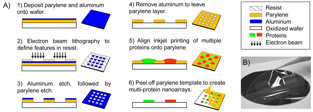
In this study, we nanofabricated parylene templates with openings down to sub-100nm feature sizes and utilized these templates to pattern protein features with high pattern fidelity. The Print-and-Peel (PNP) approach is a straightforward nanopatterning approach that combines the high-throughput and scalability of inkjet printing with the simple and uniform patterning capability of parylene peel-off. Using our PNP approach, we could rapidly generate multi-component nanoarrays of antibodies, thereby addressing the limitations of existing patterning methods. This was achieved through the consistent alignment of the inkjet printing on the fabricated parylene template, such that each printed spot optimally covered a set of nanoscopic openings in the parylene. After inkjet printing proteins, the parylene was easily peeled off to leave uniformly patterned arrays of nanoscale protein features, as shown in Figure 1. An important extension of our aligned printing process is the ability to overlay spots with different biomolecular compositions onto one another to generate combinatorial nanoarrays of increasing complexity.
Figure 1.
(a) Fabrication process of the parylene template and the PNP process to generate the protein nanoarrays. Schematic diagrams are not drawn to scale. (b) Mechanically peeling off the parylene template from a 4” wafer substrate. For the ease of illustration, the parylene peeling is shown in dry conditions, but the protein nanopatterning and parylene peeling were performed in aqueous environments that did not require drying.
The fabrication process of the parylene template is outlined in Figure 1A. A thin layer of parylene-C from Uniglobe Kisco was conformally vapor coated onto a 4” oxidized silicon wafer (Specialty Coating Systems). Virtually any substrate that is vacuum compatible can be used, such as microscope slides, coverslips etc. Thereafter, an aluminum (Al) 15nm thin film was thermally evaporated on top of the parylene. Zeon ZEP-520 resist spun to a 100nm thickness on top of the Al, was baked at 90°C, and exposed by electron beam lithography (EBL) using the JEOL JBX-9300FS. The resist was then developed in n-amyl acetate for 45 seconds and rinsed for 30 seconds in methyl isobutyl ketone and 2-isopropanol. The patterns in the resist were transferred into the Al film using reactive ion etching with Cl2/BCl3/CF4 chemistry in a PlasmaTherm 740 etcher. Finally, the nanoscale openings were transferred into the parylene using the patterned Al film as a hard etch mask and oxygen plasma reactive ion etching with the Oxford PlasmaLab 80+ etcher. The Al film was dissolved in MIF300 developer, leaving the parylene template on the wafer.
We were able to pattern nanoscale openings in the parylene template, down to sub-100nm dimension using our nanofabrication approach. This is the first demonstration of fabricating parylene templates with such fine resolution, which represents a novel lithographic process in several aspects. Firstly, the smallest opening size that we could pattern in parylene was limited by the parylene thickness and the accessibility of the oxygen plasma into the openings during etching. The ability to create nanoscale features in parylene is not obvious since previous work using parylene peel-off for biological patterning typically utilized parylene with thicknesses around 1µm or more,29, 30, 32–35 which would inhibit the creation of sub-100nm openings in the parylene template. To effectively etch through nanoscale openings in the parylene, we found that the aspect ratio (depth:width) of the openings should not exceed 4:1 for plasma accessibility. Moreover, ultra-thin parylene coatings with thickness less than 200nm have been reported to display porous behavior that was tuned to control drug elution.36 Clearly there is a benefit to having the parylene be as thin as possible for the lithographic purpose of creating the smallest features, but at the same time the parylene must be thick enough to achieve its aim as a pin-hole free patterning template. We utilized parylene with a thickness of 400nm in our work, which we found to be non-porous and yet thin enough for our lithographic purpose. Secondly, our use of the 15nm Al etch mask was different from previous work involving parylene peel-off whereby photoresist was used as the etch mask.29–33 Al was an ideal etch mask because it forms a stable oxide layer in the presence of oxygen and maintains etch anisotropy, which prevents lateral widening of the features during pattern transfer into parylene. This lateral widening can be insignificant during the fabrication of micrometer-sized openings in parylene with a photoresist etch mask, but inhibits the accurate reproduction of critical feature dimensions when creating nanometer-sized openings. The ultra-thin Al layer was important for reducing the Al etch time for pattern transfer, thus minimizing lateral widening during Al etch. However, the oxide layer prevented Al from being etched efficiently by the chlorine etch chemistry during the pattern transfer from the ZEP-520 resist layer into the Al film. We had to perform a breakthrough step at a high power of 450V to remove this oxide layer before the Al film could be etched through. This breakthrough step in turn removed the ZEP-520 resist at a faster rate. Thus, the limit of the smallest feature size we could fabricate in the parylene template was a function of the etch selectivity, anisotropy, and aspect ratio of the etching steps in the nanofabrication. The lithography used for fabricating the parylene templates is not limited to EBL, and could include other super high-resolution lithography such as nanoimprint lithography (NIL).37 NIL can potentially achieve lithographic resolution similar to EBL, but additionally pattern the same area with high throughput. We are currently exploring the use of NIL as an alternative lithographic method to imprint into the resist for the nanofabrication of our parylene templates.
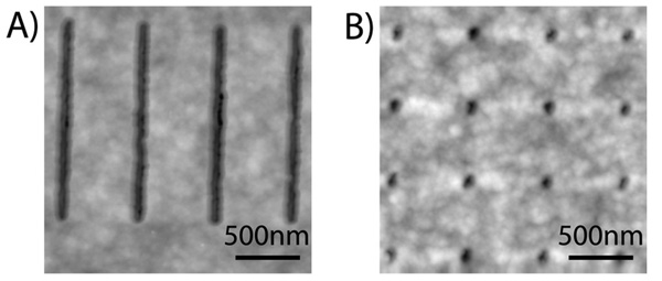
We performed tapping mode AFM using a Digital Instruments 3100 system with a silicon TESP tip at scan speeds of 0.5–2Hz to characterize the nanoscale openings fabricated in the parylene template. The AFM images were post-analyzed using the WSxM v3.0 freeware from Nanotec Electronica. The full-width-at-half-maximum (FWHM) of the cross-sectional profile of a feature was reported as its width to minimize the effect of tip convolution. In Figure 2, the AFM images of arrays of 90nm spots and 180nm lines showed that we could create nanoscopic openings of different shapes and sizes in the parylene template, due to our new fabrication process utilizing EBL and an Al hard etch mask. Furthermore, the parylene layer was observed to be non-porous, indicating that the 400nm parylene thickness was appropriate for an effective patterning template.
Figure 2.
AFM images showing arrays of nanoscale openings nanofabricated in the parylene templates – (a) 180nm lines and (b) 90nm spots. The parylene template is pinhole-free at 400nm thickness.
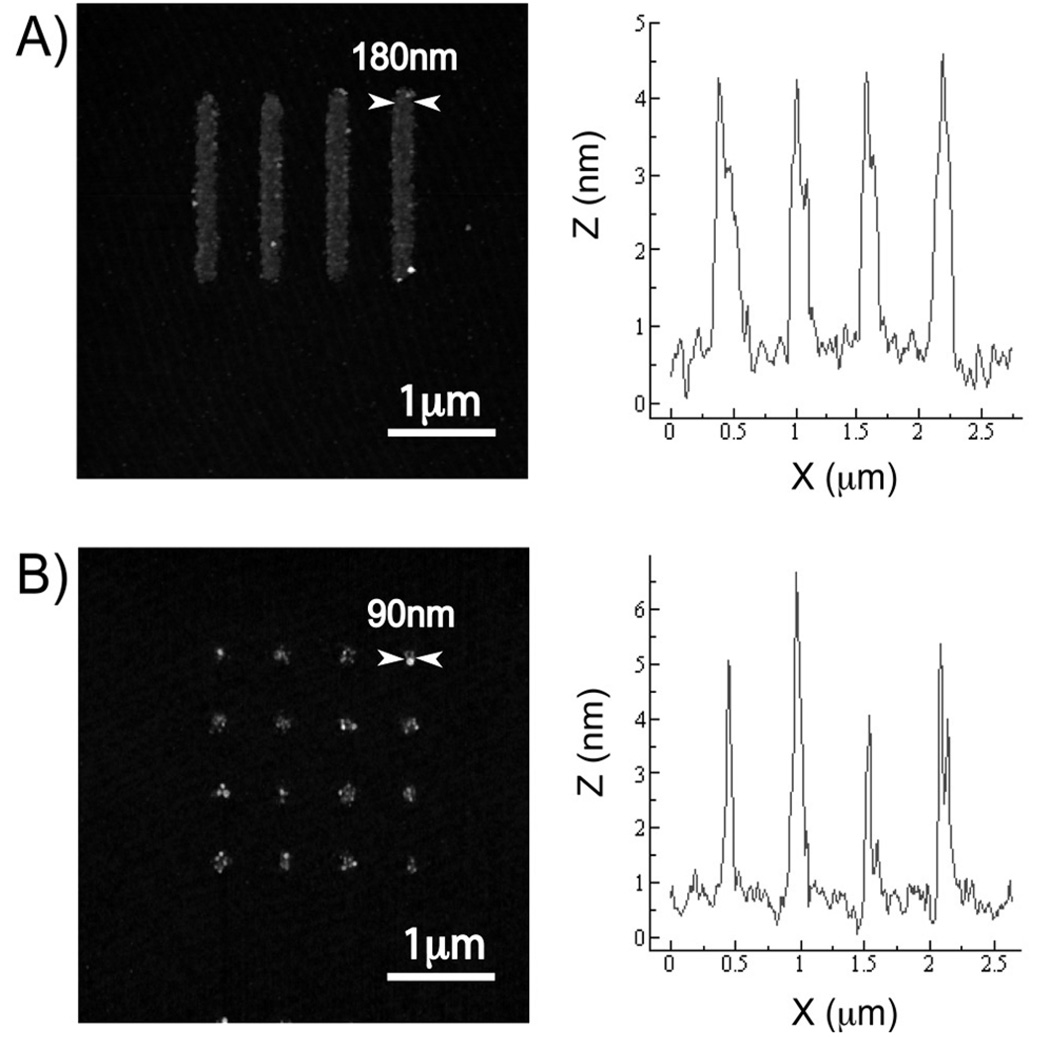
Next, we wanted to demonstrate the use of our nanofabricated parylene template to pattern nanoarrays of proteins with high fidelity. Fibronectin is a protein component of the ECM that interacts with integrins present on the surfaces of cells. We chose to pattern fibronectin as a model ECM protein because it is involved in many biological processes controlling cell fate and behavior.7, 8, 15, 29 Human fibronectin from Sigma-Aldrich was dissolved in deionized water and diluted in phosphate buffered saline to 10 µg/mL. The diluted fibronectin was manually spotted onto the parylene template, incubated for 2 hours, and rinsed with water to remove excess unbound fibronectin. The parylene was peeled off with tweezers under water to define an array of nanoscale fibronectin features. The array was kept in hydrated conditions throughout the patterning to preserve the 3D conformation and functionality of the protein. The AFM images taken of the fibronectin arrays in Figure 3 showed high fidelity patterns lines with 180 ± 13 nm widths and spots with 90 ± 18 nm diameters. We also performed a control experiment whereby buffer alone was incubated onto the parylene template. The control AFM images showed a smooth surface within the openings (data not shown), indicating that arrays of fibronectin were indeed patterned in Figure 3. This is the first time that the parylene peel-off approach has been demonstrated for patterning arrays of nanoscale protein features. Because of the chemical inertness of parylene and its resistance to swelling in hydrated environments, the antibody features were replicated with high fidelity, nanoscale resolution. The cross-sectional height profile of the fibronectin features shows a relatively uniform height distribution of 4–5nm, comparable to another prior study.38 We postulate that the apparent heterogeneity within each 90nm spot was due to fibronectin aggregates being adsorbed, since fibronectin has been reported to adopt a compact globular structure under low ionic strength.38 In the future, reducing the feature size of patterned ECM proteins to nanoscale dimensions may help improve the resolution of studies in cell polarity and focal adhesion formation.9, 39
Figure 3.
AFM images and the cross-sectional profiles of patterned fibronectin nanoarrays – (a) 180nm lines and (b) 90nm spots. The fibronectin patterns were replicated with high fidelity from the parylene templates. The cross-sectional profiles were taken from a span across four array features on each image, and the FWHM of each peak was measured as the feature width. The heights of the patterned fibronectin features were relatively uniform at 4–5nm.
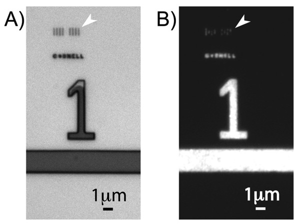
We performed fluorescent immunostaining to further confirm the biological activity and presence of the patterned fibronectin features. Figure 4A shows a differential contrast microscopy image of the original parylene template with both microscopic and nanoscopic openings. The micrometer-sized number and line were used to help locate the 180nm nanoscale lines demarcated by the arrows. After parylene peel-off, rabbit anti-fibronectin antibody from Sigma-Aldrich and Alexa Fluor 488 conjugated goat anti-rabbit secondary antibody from Invitrogen were used to immunostain the fibronectin features following the manufacturers’ protocols. Fluorescent features were observed in Figure 4B, indicating that we had successfully patterned fibronectin with high fidelity and also preserved the functionality of the protein. The 90nm spot openings and fluorescent features could not be visualized by optical microscopy because the feature size was drastically smaller than the diffraction limit. It was however possible to see the dim fluorescence of the 180nm lines demarcated by the arrows in Figure 4B.
Figure 4.
Fluorescent immunostaining to confirm the presence and functionality of patterned fibronectin. (a) Differential contrast microscopy image of the original parylene template, with arrays of 180nm lines marked by the arrow. (b) Fluorescence microscopy image showing immunostaining of the fibronectin features successfully patterned onto the surface. The image brightness and contrast have been adjusted, so that the dim fluorescence of the lines demarcated by the arrow could be seen. The arrays of 90nm spots could not be easily visualized by optical microscopy since their size is significantly smaller than the diffraction limit.
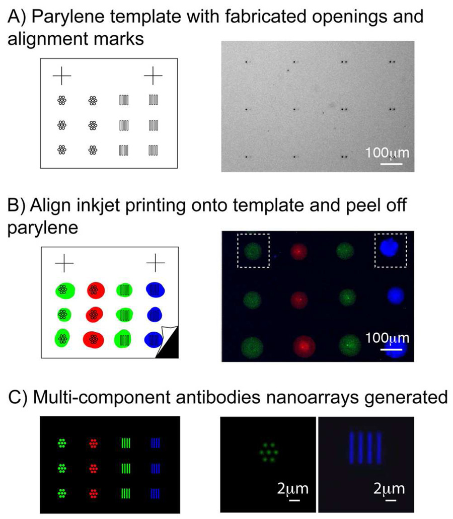
We developed the PNP approach to take advantage of the high-throughput, multiplexing capabilities of inkjet printing with the nanopatterning ability of parylene peel-off. The right image in Figure 5A shows a bright field microscopy image of a portion of the fabricated parylene template. We utilized alignment marks – microscale crosses with line widths of 20µm and lengths of 100µm created in the parylene template – to help locate the positions of the nanoscale openings in the parylene using a high magnification microscope camera. We were able to achieve visual alignment accuracies down to 20µm, although this can be easily improved by using a camera with high magnification. The coordinates of the nanoscale features were calculated and used to program the inkjet arrayer for aligned printing of the antibodies spots onto the parylene openings. While we have used an inkjet printer, our PNP technique would also work for other printing technologies, such as quill-pin spotting and contact printing. Various antibodies tagged with different fluorophores – Alexa Fluor 488 goat anti-rabbit IgG, Alexa Fluor 555 goat anti-rabbit IgG, and Alexa Fluor 647 goat anti-mouse IgG – were diluted in 1:100 v/v in 50% glycerol printing buffer. Each diluted antibody was loaded into a well in a 384-wells microplate and then printed with alignment using the Marathon Inkjet Microarrayer from Arrayjet. For simplifying the fluorescence colors, only three different fluorescent antibodies were used in our experiment, however 1,000s of different species can be loaded into several microplates and routinely printed as indicated in the inkjet printer specifications provided by the manufacturer. Each printed spot of antibody ~70–100µm covers a set of nanoscopic openings in the parylene template, as shown in Figure 5B. Three pre-assembled filter cubes from Chroma and Omega Optical were used to collect the fluorescence images, with each cube designed to image one specific fluorophore. The images collected from the three fluorescence channels were overlaid using ImageJ (National Institutes of Health). The final merged image was pseudo-colored – Alexa Fluor 488 (green), Alexa Fluor 555 (blue), and Alexa Fluor 647 (red) – to illustrate the different antibodies patterned.
Figure 5.
The PNP process. Schematic diagram of each step is shown on the left, not drawn to scale. (a) Bright field microscopy image showing a part of the parylene template pre-defined with openings and alignment marks. (b) Pseudo-color merged fluorescence image showing aligned inkjet printing of different antibodies onto parylene. (c) Multi-component antibodies arrays were generated after peel off, corresponding to the boxed region in (b). Array features of different shapes and sizes – 600nm wide lines and spots –were patterned with the PNP process.
As illustrated in Figure 5C, the parylene template was then mechanically peeled away to uniformly pattern multi-component antibodies arrays with different nanoscale feature shapes and sizes. Arrays of 600nm lines and 600nm spots of antibodies could be patterned, as shown in Figure 5C, despite inconsistencies in the original inkjet spot morphology and size. We demonstrate that our PNP process could be used to clean-up imperfect inkjet printed spots by transforming them into consistently defined features through the application of the parylene template. We note that this spot transformation is not limited to nanoscale features, and can also be used to pattern microscale features, provided that the original inkjet spot is larger than the openings in the parylene. Our simple alignment approach in the PNP process enables multiple species to be reproducibly patterned onto a surface, circumventing the problem of alignment issues associated with printing multiple components in µCP. Our PNP technology can extend the resolution of regular inkjet printing from micrometers to sub-micrometers, after a single straightforward peeling step to remove the parylene template. Furthermore PNP can be scaled up to print 1,000s of different components with a high throughput associated with standard microarrayers. The spacing between each set of patterned antibody features in our nanoarrays is currently limited by the 70–100µm diameter of the inkjet printed spot on our hydrophobic parylene surface. Based on this spacing, we calculated that over 20,000 different antibodies could be printed on a 1cm × 2cm chip area at maximum packing density. We are currently working to reduce this spacing to sub-micrometers and achieve an even higher packing density by utilizing a multilayer parylene template.40 This work is the first demonstration where multiple proteins are arrayed on a single surface utilizing parylene peel-off, while previous work involving bath incubation of solutions onto the parylene template have been limited to patterning arrays containing at most two different proteins.30 Antibodies arrays created using our PNP method could be used for immunoassays, molecular diagnostics, and cytokines screening.
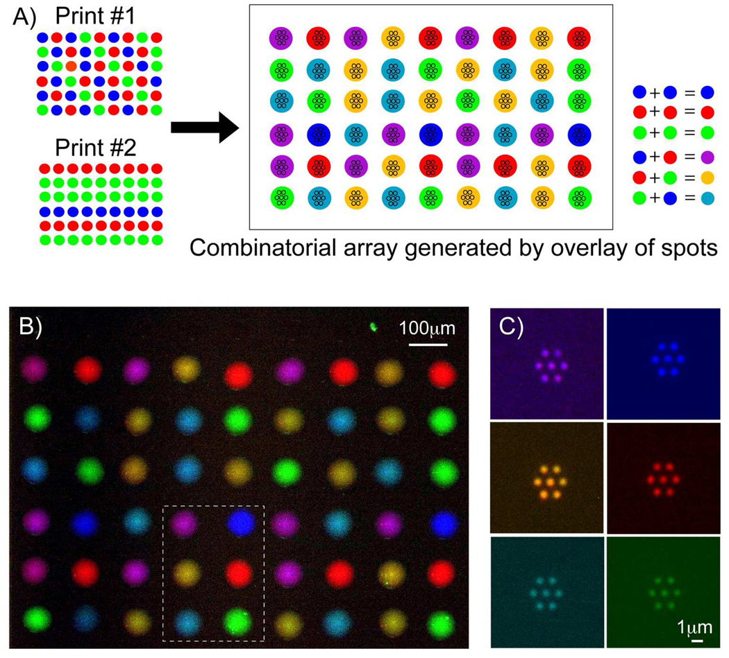
Our aligned printing process allows us to dramatically extend the utility of these PNP arrays by offering a convenient alternative method to create nanoarrays of mixed proteins. We superimposed the printing of a second set of spots immediately on top of the first set, to create arrays with different combinations of antibodies per feature, as illustrated in the schematic in Figure 6A. The fluorescence images of the inkjet printed spots corresponding to the three fluorophores were collected and merged to yield a pseudo-color image in Figure 6B. Six different combinations of antibodies could be generated from an initial pool of three different antibodies. After parylene peel-off, arrays of 600nm diameter spots containing various combinations of antibodies were patterned in Figure 6C. These experiments show that we can potentially increase the combinations of biomolecules patterned by increasing the number of different types of antibodies in the initial pool, followed by overlaying more sets of spots per array feature. Although we have used purified proteins and antibodies for these experiments, any desired biomaterials ranging from nucleic acids to cells and cell lysates, can be printed in combination or by itself. Arraying different combinations of biomolecular components has been important in combinatorial screening of pharmaceutical compounds and responses of stem cells to various polymeric surfaces, signaling, growth or transfection cues.16, 17, 41 The ability of our PNP technology to create combinatorial biomolecular nanoarrays with ease and high throughput will open up the opportunity to explore synergistic and antagonistic combinations of biomolecules in receptor-ligand interactions.
Figure 6.
The PNP process can generate combinatorial biomolecular nanoarrays. (a) Schematic diagram showing the process of superimposing a second inkjet print-run immediately over the first print to generate six different combinations of antibodies from an initial pool of three separate antibodies. (b) Pseudo-color merged fluorescence image showing the combinatorial array that can be inkjet printed onto the parylene template. (c) Antibodies nanoarrays of six different biomolecular combinations were generated after parylene peel-off, corresponding to the spots demarcated within the boxed region in (b).
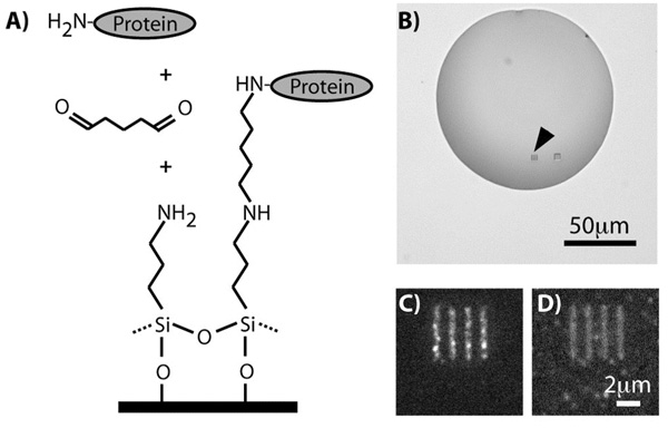
We further modified our PNP technique to covalently link smaller proteins to the oxidized silicon surface exposed in the parylene openings. While large proteins such as fibronectin (450kDa) and immunoglobulin antibodies (150kDa) can irreversibly adsorb to a surface, smaller proteins may desorb again from surfaces after adsorption,42 necessitating covalent linkage. Following oxygen plasma etching of our parylene chips, we functionalized the oxidized silicon surfaces with 10% 3-aminopropyltriethoxysilane in anhydrous toluene for 1 hour, followed by rinsing in toluene, methanol, and water for 15 mins. The chips were then treated with 2.5% glutaraldehyde, a homobifunctional linker that would covalently cross-link amine groups on the silane and protein. The schematic in Figure 7A shows our method for this surface chemistry, which is modified from literature.43 Small proteins, namely recombinant human interleukin-8 (IL-8, 8kDa, R&D sytems) and tissue growth factor alpha (TGF-α, 5.5kDa, Abcam) were inkjet printed onto the parylene chips at 1µM and incubated for 1 hour. Figure 7B shows an inkjet droplet containing IL-8 covering an array of nanoscale line features demarcated by the black arrow. The chips were blocked with 1% bovine serum albumin in phosphate buffered saline for 1 hour. Fluorescent immunostaining was performed using goat anti-IL-8 antibody (R&D systems) and mouse anti-TGF-α antibody (Abcam), and secondary fluorescent Alexa 647-conjugated donkey anti-mouse and Alexa 488-conjugated donkey anti-goat antibody, following manufacturers’ instructions. The fluorescent images in Figures 7C and 7D correspond to TGF-α and IL-8 patterned chips collected at the appropriate emission wavelengths respectively. Our results demonstrate that our PNP technique can be utilized for nanopatterning arrays of covalently bound proteins, as confirmed by fluorescence immunostaining using antibodies that specifically recognize IL-8 and TGF-α.
Figure 7.
(a) Schematic showing the surface modification of our parylene chips utilizing 3-aminopropyltriethoxysilane and glutaraldehyde for covalently immobilizing proteins. (b) Brightfield image of an inkjet droplet of IL-8 incubated on the parylene openings that have been treated with glutaraldehyde and aminosilane. (c) Fluorescent image collected in the 647nm emission wavelength following immunostaining, showing TGF-α covalently bound to the surface as a nanoarray of 600nm line features. (d) Fluorescent image similar to (c) but for IL-8 and collected in the 488nm emission wavelength.
In conclusion, we have developed a PNP technology that is capable of producing nanoscale resolution, multi-component biomolecular arrays. These arrays can be rapidly produced in a large area format with high throughput using standard inkjet printers or microarrayers utilized in the PNP process. Uniform nanoscale array features can be patterned despite imperfections in the inkjet spot morphologies. The aligned printing process can be further extended to create combinatorial nanoarrays, as well as nanoarrays of covalently linked proteins. We anticipate that these multi-component biomolecular nanoarrays will be useful for high-resolution studies of subcellular biological processes and interactions, integrating biochemical functionalities with nanoscale sensors, and engineering cellular and tissue micro- and nanoenvironments.
ACKNOWLEDGMENT
The authors are grateful to Rob Ilic and Vince Genova for helpful discussions on nanofabrication, and Daniel Brooks for the immunostaining protocol. C.P.T. and B.R.C. are supported by NIH DC07489 and DA025722 respectively. The nanofabrication was performed in part at the Cornell NanoScale Facility, a member of the National Nanotechnology Infrastructure Network, which is supported by NSF ECS-0335765.
REFERENCES
- 1.Khademhosseini A, Borenstein J, Toner M, Takayama S, editors. Micro and Nanoengineering of the Cell Microenvironment. Boston, MA: Artech House; 2008. [Google Scholar]
- 2.Blattler T, Huwiler C, Ochsner M, Stadler B, Solak H, Voros J, Grandin HM. J. of Nanosci. and Nanotechnol. 2006;6(8):2237–2264. doi: 10.1166/jnn.2006.501. [DOI] [PubMed] [Google Scholar]
- 3.Lee KB, Park SJ, Mirkin CA, Smith JC, Mrksich M. Science. 2002;295(5560):1702–1705. doi: 10.1126/science.1067172. [DOI] [PubMed] [Google Scholar]
- 4.Takayama S, Ostuni E, LeDuc P, Naruse K, Ingber DE, Whitesides GM. Nature. 2001;411(6841):1016–1016. doi: 10.1038/35082637. [DOI] [PubMed] [Google Scholar]
- 5.Senaratne W, Sengupta P, Jakubek V, Holowka D, Ober CK, Baird B. J. Am. Chem. Soc. 2006;128(17):5594–5595. doi: 10.1021/ja058701p. [DOI] [PubMed] [Google Scholar]
- 6.Torres AJ, Wu M, Holowka D, Baird B. Ann. Rev. Biophys. 2008;37:265–288. doi: 10.1146/annurev.biophys.36.040306.132651. [DOI] [PubMed] [Google Scholar]
- 7.Goffin JM, Pittet P, Csucs G, Lussi JW, Meister JJ, Hinz B. J. Cell Biol. 2006;172(2):259–268. doi: 10.1083/jcb.200506179. [DOI] [PMC free article] [PubMed] [Google Scholar]
- 8.Chen CS, Mrksich M, Huang S, Whitesides GM, Ingber DE. Science. 1997;276(5317):1425–1428. doi: 10.1126/science.276.5317.1425. [DOI] [PubMed] [Google Scholar]
- 9.Arnold M, Cavalcanti-Adam EA, Glass R, Blummel J, Eck W, Kantlehner M, Kessler H, Spatz JP. ChemPhysChem. 2004;5(3):383–388. doi: 10.1002/cphc.200301014. [DOI] [PubMed] [Google Scholar]
- 10.Cui Y, Wei QQ, Park HK, Lieber CM. Science. 2001;293(5533):1289–1292. doi: 10.1126/science.1062711. [DOI] [PubMed] [Google Scholar]
- 11.Domansky K, Li J, Janata J. J. Electrochem. Soc. 1997;144(4):L75–L78. [Google Scholar]
- 12.Waggoner PS, Craighead HG. Lab Chip. 2007;7:1238–1255. doi: 10.1039/b707401h. [DOI] [PubMed] [Google Scholar]
- 13.St John PM, Davis R, Cady N, Czajka J, Batt CA, Craighead HG. Anal. Chem. 1998;70(6):1108–1111. doi: 10.1021/ac9711302. [DOI] [PubMed] [Google Scholar]
- 14.MacBeath G, Schreiber SL. Science. 2000;289(5485):1760–1763. doi: 10.1126/science.289.5485.1760. [DOI] [PubMed] [Google Scholar]
- 15.Flaim CJ, Chien S, Bhatia SN. Nat. Methods. 2005;2(2):119–125. doi: 10.1038/nmeth736. [DOI] [PubMed] [Google Scholar]
- 16.Yoshikawa T, Uchimura E, Kishi M, Funeriu DP, Miyake M, Miyake J. J. Controlled Release. 2004;96(2):227–232. doi: 10.1016/j.jconrel.2004.01.024. [DOI] [PubMed] [Google Scholar]
- 17.Anderson DG, Levenberg S, Langer R. Nat. Biotechnol. 2004;22(7):863–866. doi: 10.1038/nbt981. [DOI] [PubMed] [Google Scholar]
- 18.Bailey SN, Ali SM, Carpenter AE, Higgins CO, Sabatini DM. Nat. Methods. 2006;3(2):117–122. doi: 10.1038/nmeth848. [DOI] [PubMed] [Google Scholar]
- 19.Zhu H, Snyder M. Curr. Opin. Chem. Biol. 2003;7(1):55–63. doi: 10.1016/s1367-5931(02)00005-4. [DOI] [PubMed] [Google Scholar]
- 20.Huo FW, Zheng ZJ, Zheng GF, Giam LR, Zhang H, Mirkin CA. Science. 2008;321(5896):1658–1660. doi: 10.1126/science.1162193. [DOI] [PMC free article] [PubMed] [Google Scholar]
- 21.Mei Y, Cannizzaro C, Park HS, Xu QB, Bogatyrev SR, Yi K, Goldman N, Langer R, Anderson DG. Small. 2008;4(10):1600–1604. doi: 10.1002/smll. [DOI] [PMC free article] [PubMed] [Google Scholar]
- 22.Coyer SR, Garcia AJ, Delamarche E. Angew. Chem., Int. Ed. 2007;46(36):6837–6840. doi: 10.1002/anie.200700989. [DOI] [PubMed] [Google Scholar]
- 23.Tien J, Nelson CM, Chen CS. Proc. Natl. Acad. Sci. U.S.A. 2002;99(4):1758–1762. doi: 10.1073/pnas.042493399. [DOI] [PMC free article] [PubMed] [Google Scholar]
- 24.Roth EA, Xu T, Das M, Gregory C, Hickman JJ, Boland T. Biomaterials. 2004;25(17):3707–3715. doi: 10.1016/j.biomaterials.2003.10.052. [DOI] [PubMed] [Google Scholar]
- 25.Lee KB, Lim JH, Mirkin CA. J. Am. Chem. Soc. 2003;125(19):5588–5589. doi: 10.1021/ja034236p. [DOI] [PubMed] [Google Scholar]
- 26.Braunschweig AB, Huo FW, Mirkin CA. Nat. Chemistry. 2009;1(5):353–358. doi: 10.1038/nchem.258. [DOI] [PMC free article] [PubMed] [Google Scholar]
- 27.Zheng ZJ, Daniel WL, Giam LR, Huo FW, Senesi AJ, Zheng GF, Mirkin CA. Angew. Chem., Int. Ed. 2009;48(41):7626–7629. doi: 10.1002/anie.200902649. [DOI] [PMC free article] [PubMed] [Google Scholar]
- 28.Wang YH, Giam LR, Park M, Lenhert S, Fuchs H, Mirkin CA. Small. 2008;4(10):1666–1670. doi: 10.1002/smll.200800770. [DOI] [PMC free article] [PubMed] [Google Scholar]
- 29.Tan CP, Seo BR, Brooks DJ, Chandler EM, Craighead HG, Fischbach C. Integrative Biology. 2009;1(10):587–594. doi: 10.1039/b908036h. [DOI] [PubMed] [Google Scholar]
- 30.Ilic B, Craighead HG. Biomed. Microdevices. 2000;2(4):317–322. [Google Scholar]
- 31.Moran-Mirabal JM, Tan CP, Orth RN, Williams EO, Craighead HG, Lin DM. Anal. Chem. 2007;79(3):1109–1114. doi: 10.1021/ac061898z. [DOI] [PMC free article] [PubMed] [Google Scholar]
- 32.Moran-Mirabal JM, Edel JB, Meyer GD, Throckmorton D, Singh AK, Craighead HG. Biophys. J. 2005;89(1):296–305. doi: 10.1529/biophysj.104.054346. [DOI] [PMC free article] [PubMed] [Google Scholar]
- 33.Orth RN, Wu M, Holowka DA, Craighead HG, Baird BA. Langmuir. 2003;19(5):1599–1605. [Google Scholar]
- 34.Jinno S, Moeller HC, Chen CL, Rajalingam B, Chung BG, Dokmeci MR, Khademhosseini A. J. Biomed. Mater. Res., Part A. 2008;86A(1):278–288. doi: 10.1002/jbm.a.32030. [DOI] [PubMed] [Google Scholar]
- 35.Wright D, Rajalingam B, Selvarasah S, Dokmeci MR, Khademhosseini A. Lab Chip. 2007;7:1272–1279. doi: 10.1039/b706081e. [DOI] [PubMed] [Google Scholar]
- 36.Lam R, Chen M, Pierstorff E, Huang H, Osawa EJ, Ho D. ACS Nano. 2008;2(10):2095–2102. doi: 10.1021/nn800465x. [DOI] [PubMed] [Google Scholar]
- 37.Chou SY, Krauss PR, Renstrom PJ. Science. 1996;272(5258):85–87. [Google Scholar]
- 38.Bergkvist M, Carlsson J, Oscarsson S. J. Biomed. Mater. Res., Part A. 2003;64A(2):349–356. doi: 10.1002/jbm.a.10423. [DOI] [PubMed] [Google Scholar]
- 39.Thery M, Racine V, Piel M, Pepin A, Dimitrov A, Chen Y, Sibarita JB, Bornens M. Proc. Natl. Acad. Sci. U.S.A. 2006;103(52):19771–19776. doi: 10.1073/pnas.0609267103. [DOI] [PMC free article] [PubMed] [Google Scholar]
- 40.Kuribayashi K, Hiratsuka Y, Yamamura T, Takeuchi S. IEEE MEMS 2007. 2007:501–504. [Google Scholar]
- 41.Angres B. Expert Review of Molecular Diagnostics. 2005;5(5):769–779. doi: 10.1586/14737159.5.5.769. [DOI] [PubMed] [Google Scholar]
- 42.Sigal GB, Mrksich M, Whitesides GM. J. Am. Chem. Soc. 1998;120(14):3464–3473. [Google Scholar]
- 43.Tlili A, Jarboui MA, Abdelghani A, Fathallah DM, Maaref MA. Materials Science & Engineering C-Biomimetic and Supramolecular Systems. 2005;25(4):490–495. [Google Scholar]


