Abstract
The miniaturization of nano-scale electronic devices, such as metal oxide semiconductor field effect transistors (MOSFETs), has given rise to a pressing demand in the new theoretical understanding and practical tactic for dealing with quantum mechanical effects in integrated circuits. Modeling and simulation of this class of problems have emerged as an important topic in applied and computational mathematics. This work presents mathematical models and computational algorithms for the simulation of nano-scale MOSFETs. We introduce a unified two-scale energy functional to describe the electrons and the continuum electrostatic potential of the nano-electronic device. This framework enables us to put microscopic and macroscopic descriptions in an equal footing at nano scale. By optimization of the energy functional, we derive consistently-coupled Poisson-Kohn-Sham equations. Additionally, layered structures are crucial to the electrostatic and transport properties of nano transistors. A material interface model is proposed for more accurate description of the electrostatics governed by the Poisson equation. Finally, a new individual dopant model that utilizes the Dirac delta function is proposed to understand the random doping effect in nano electronic devices. Two mathematical algorithms, the matched interface and boundary (MIB) method and the Dirichlet-to-Neumann mapping (DNM) technique, are introduced to improve the computational efficiency of nano-device simulations. Electronic structures are computed via subband decomposition and the transport properties, such as the I-V curves and electron density, are evaluated via the non-equilibrium Green's functions (NEGF) formalism. Two distinct device configurations, a double-gate MOSFET and a four-gate MOSFET, are considered in our three-dimensional numerical simulations. For these devices, the current fluctuation and voltage threshold lowering effect induced by the discrete dopant model are explored. Numerical convergence and model well-posedness are also investigated in the present work.
1 Introduction
The continuous demand in rising the performance of electronic devices has led to the reduced geometric dimension and supply voltage of metal oxide semiconductor field effect transistors (MOSFETs), or complementary metal oxide semiconductors (CMOSs), which are fundamental building blocks of large scale integrated circuits used in almost all electronic equipments. At present, MOSFETs are designed, manufactured and operating at much less than 100nm scale. According to “International Technology Roadmap for Semiconductors (ITRS) (http://www.itrs.net/)”, the channel length of CMOSs will be down scaled from the present 45 to about 22 nm in 2016. The down-scaling of the transistor channel length also requires simultaneous down-scaling of the gate oxide, connecting material, doping concentration and operation voltages [30, 20, 13]. The ultimate channel length is expected to be around 16 nm. At such a channel length, most critical design parameters quickly approach the atomic scale and associated physical limits. Many down-scaling associated devices characteristics have been studied by Vasileska, et al [3, 2, 41, 42, 55, 43, 56] for MOSFET, FinFET and various other silicon on insulator (SOI) devices. The most important feature of a nano-scale transistor is that quantum mechanical effects become significant and will dramatically impact the macroscopic quantities, such as current-voltage characteristics and conductance. In particular, at 22 nm or less, channel tunneling and gate leakage may devastate the classical function of the MOSFET. Electrostatic control and suppression of quantum effects are important issues [76, 85, 29, 21, 88, 49, 4, 27, 82, 25, 8, 94]. Nano transistors with the range of channel lengths being around 20 nm and 10 nm are referred as “ultimate CMOSs” and “functionally enhanced CMOSs”, respectively. Ultimate CMOSs are the smallest CMOSs that still operate with the classical principle while severe quantum effects have to be suppressed by appropriate electrostatic potentials and designs. Functionally enhanced CMOSs are nano-quantum transistors which utilize the fundamental properties of nature that do not have direct analogs in classical physics. Some of these properties are quantum coherence, i.e., a possibility for a quantum system to occupy several states simultaneously, and quantum correlation or entanglement. Presently, the majority of these quantum structures, such as nano-mechanical resonators, quantum dots, quantum wires, single electron transistors, and similar low dimensional structures, exist only as prototypes in research laboratories or just being contemplated [52, 34]. The working principle and physical function of quantum devices are subjects of extensive research. Practical realization of quantum transistors faces a number of challenges in design, test, material selection, lithography, interconnect, process integration, metrology, assembly, packaging, plus device modeling and simulation.
The main purpose of our electronic device modeling is to predict device characteristics and performance. This amounts to the understanding of transport features, including current-voltage (I-V) characteristics at the source, drain or gate contacts of the device. For ultimate MOSFETs and other nano-quantum transistors, quantum effects, such as gate leakage and channel tunneling under various voltage settings will be of main concerns of the modeling and simulation [59, 91]. Currently, the non-equilibrium Green's functions (NEGF) formalism is the main workhorse for nano-device transport modeling [96, 45]. The NEGF formalism was originally developed by Schwinger [87], Kadanoff and Baym [54], and has been revived recently for device modeling [23, 59, 22, 91]. This is a general and useful formalism using the Fermi-Dirac statistics for electrons. It allows the description of interactions, including scattering processes of particles (i.e., electrons and phonons) and relaxation due to the surroundings. An equivalent approach is the Dyson integral equation representation. However, computational aspects for differential and integral equations are quite different. Another practical transport model is the Boltzmann equation, or the Boltzmann-Vlasov equation, which describes the kinetic of a typical particle, such as electron, phonon, or photon, due to the two-body scattering with another particle and/or external field effect [44, 15]. The inherent Boltzmann distribution can be a good approximation to the Fermi-Dirac distribution at high temperature. Transport properties, such as current density, conductance and tunneling rate, can be computed as expectation values of physical observables with the distribution function, the Wigner distribution [51] or density operator [2]. In fact, the transport equation derived form the quantum Boltzmann equation, known as the Waldmann-Snider equation [95, 90], can provide quantum correction to the classical drift-diffusion expression. The Waldmann-Snider equation can be derived from the BBGKY hierarchy with an appropriate scattering closure for the two-body density operator. Recently, Cheng et al have constructed a discontinuous Galerkin solver for Boltzmann-Poisson systems in double-gate MOSFETs [19]. Moreover, the Bloch-Boltzmann Peierl equation can be used for the transport of electrons and polar optical phonons in periodic settings [38, 39]. Other density matrix methods, such as the Master equation [48, 35], describe the time evolution of the probability function. Yet another approach is the Fokker-Planck equation describing the rate change of the probability density function of a particle in terms of drift-diffusion processes [76, 85, 73]. This equation can be used to model the electron transport in the quantum ballistic regime [74]. Some quantum corrected classical methods, such as quantum drift-diffusion (QDD) models or Schrödinger-Poisson drift-diffusion (SPDD) models, are employed and summarized in a unified framework [24, 27]. The well-posedness of these models and numerical efficiency are analyzed mathematically in the fashion of solution fixed point maps [27]. Additionally, Monte Carlo methods have also been applied to electron transport [15, 3, 55]. The electron scattering effect from the devices interface roughness was studied via an ensemble Monte Carlo device simulation technique [56]. A new scheme was proposed and applied to study the role of the discrete impurities in the device terminal characteristics [41, 43, 42]. By using a corrected Coulomb force, this approach prevents the double-counting of the electron-electron and electron-ion long-range interaction.
To account for the quantum effect, the electronic structure in terms of wavefunctions is required in most transport evaluations. The quantum mechanical theory is indispensable for electron structures at nano scale. Although formally a fully quantum mechanical first principle description is desirable for a given device feature at nano scale, it normally involves a large number of atoms, molecules and electrons, therefore the resulting full scale quantum system is intractable. Appropriate approximations are required. At the lowest level of approach, a single electron dynamics in a band structure of the solid is governed by the Schrödinger equation, which is coupled back to the Poisson equation as charge sources [69, 92, 11, 53, 62, 6, 32, 86, 10]. The interaction of many bands can also be considered by using a general k · p method derivation of many-body Schrödinger equation [106, 34, 70]. Recently, linear combination of bulk band (LCBB) method [49], which relies on the expansion of the confined states in terms of periodic Bloch wave functions, was used for a large number of atoms. The solution of the many-electron Schrödinger equation, including atomic information, is extremely expensive. Semi-empirical approaches which make use of parameters from experimental data are often used. More rigorous but expensive methods are ab-initio approaches, including the Hartree-Fock method [89] and the density functional theory (DFT) [46, 58, 77]. The size of the system is limited when ab-initio methods are used. To increase the computational capability, pseudopotential methods can be used to remove core electrons and singularities in calculations. The resulting quantum mechanical system is still formidably expensive to solve for nano devices. The DFT is associated with the Kohn-Sham equation and it can be accelerated by using the linear scaling divide and conquer method [98, 65] and the tight binding approximation [47]. In general, there is a pressing need to develop innovative modeling strategies and efficient computational methods for realistic device problems.
The recent miniaturization of CMOSs or MOSFETs has led to a new era in modeling and simulation of these nano-scale devices. Apart from difficulties with device fabrication and testing which typically require nano scale resolution and high precision control, there are numerous modeling and computational problems associated with ultimate and functionally enhanced nano transistors as discussed by the ITRS. The essences of these problems are quantum effects, geometric interface effects and dopant effects. 1) Quantum effects include electron confinement, resonance states, source-drain off state quantum tunneling current, channel barrier tunneling, gate leakage, many body correlations and channel-channel interference at nano scale. These effects are commonly modeled by the coupled Poisson-Schrödinger equations. However, the consistence and validity of these equations have rarely been examined. There is a pressing need for innovative methods, models and algorithms that contribute to the prediction and design of nano-quantum transistors whose channel lengths are in the range of 8-22 nm. 2) Geometric interface effects refer to the impact of (layered) material variations within a device and interconnects between devices to the device performance. These effects become crucial to ultimate CMOSs and functionally enhanced CMOSs. For example, dielectric interfaces of metal-oxide, metal-semiconductor, and oxide-semiconductor will induce non-ballistic transport behavior even if there is no other interaction [56]. However, with few exceptions [68], most present simulation models are based on simplified rectangular geometric shapes, homogeneous dielectric media, and even reduced dimensions. The impact of realistic geometry, including gate dielectric layers and interconnects, has hardly been investigated in the past and calls for new modeling strategies and innovative methods. 3) Doping effects are often described by distribution functions in continuum device models without explicit consideration of individual dopant atoms and traps [17]. This continuum approach works very well for electronic devices of large sizes but will lead to severe errors in electron structure and transport for ultimately scaled nano devices. These errors are often seen as statistical fluctuations [57, 33]. When the device size is reduced to 22 nm or less, it becomes indispensable to consider individual dopant atoms and traps. However, with few exceptions [49, 41, 43, 42], this issue has been hardly addressed in the literature. As individual dopants are fundamental to the function of ultimate MOSFETs and nano-quantum transistors, it is imperative to develop innovative models and efficient methods to analyze their impact.
Currently in device modeling and simulation, most attention has been paid to the approximation and solution of the Schrödinger equation using either real-space meshes or atomic basis functions [88, 49, 63, 28, 82, 12, 84, 36]. Since the computational domain is usually treated as rectangular and homogeneous, the Poisson equation can be easily solved with efficient O(N) schemes, such as the fast Fourier transform (FFT) or multigrid algorithms. However, these Poisson solvers cannot be employed if one considers irregular geometry from practical design, or material interfaces from gate dielectric layers and interconnects. One has to solve the Poisson equation with discontinuous coefficients and singular sources, which is a challenging task in both mathematical and computational senses. To achieve high-order accuracy and convergence, suitable interface techniques are indispensable. Since Peskin's pioneering work, the immersed boundary method (IBM) [79, 80, 78] and a number of other elegant methods have been proposed in the literature, including the ghost fluid method (GFM) proposed by Fedkiw, Osher and coworkers [31, 67], the upwinding embedded boundary method proposed by Cai and Deng [16], finite element based formulations [9, 14, 66], finite-volume-based methods [75], and integral equation methods [72]. A major advance in the field was due to LeVeque and Li [61], who proposed a remarkable second order sharp interface scheme, the immersed interface method (IIM) [1, 64]. Recently, we have developed a highly accurate interface technique, the matched interface and boundary (MIB) method [104, 108, 107, 101, 100] for solving elliptic equations with discontinuous coefficients. The MIB is of arbitrarily high-order accuracy in principle, and sixth-order accurate MIB schemes have been demonstrated [100, 108]. It has been successfully applied to the analysis of mechanical structures [102, 105], waveguides [105] and biomedical imaging [18]. Recently, Zhao has developed a fourth-order full-vectorial MIB method for optical waveguides with smoothly curved interfaces [103]. However, most of these interface techniques have not been implemented in the context of the modeling of realistic nano devices. There is a need to develop elliptic interface techniques for nano device modeling and simulation.
The objectives of the present work are three-fold. First, we introduce a two-scale variational framework that, upon energy optimization, generates new self-consistently coupled Poisson-Kohn-Sham equations which allow the easy incorporation of linear scaling tight-binding, pseudopotential, atomic charges and dopants, divide and conquer methods. The proposed framework puts macroscopic description of electrostatic potentials and the microscopic description of electronic structures at an equal footing at nano scale. Additionally, interface models and associated elliptic interface techniques are introduced to the nano-electronic device modeling and computation. The MIB method is applied to provide accurate simulation of the coupled Poisson-Schrödinger equation systems. This method is able to deal with irregular interface shapes and geometric singularities [100]. Finally, we provide a new mathematical model to account for the random individual dopant effect in semiconductor material. The Dirac delta function is used to represent the dopant position and eliminates the finite-size effect in the previous discrete dopant models [7, 71, 50]. The computational difficulty of handling the delta function is removed by the introduction of a Dirichlet-to-Neumann mapping (DNM) technique.
The rest of this paper is organized as follows. Mathematical models for nano-electronic devices are presented in Section 2. The coupled Poisson-Schrödinger equations are derived from the variational framework and provide a rigorous starting point for electronic structure simulation. Additionally, the subband decompositions are discussed for a double-gate MOSFET and a four-gate MOSFET. The NEGF formalism is briefly described for the evaluation of transport properties, such as current-voltage relation and electron density. Moreover, a material interface model is also discussed for nano device modeling. Appropriate interface conditions are prescribed at semiconductor interfaces to ensure the continuity of the electrostatic potential and its flux. Furthermore, we describe the delta function based individual dopant formulation which allows the modeling of random dopant effect to the device transport. In Second 3, we describe computational procedures and algorithms for electronic structures and transport in nano-electronic devices. The coupled Poisson-Schrödinger equations are solved in conjunction with the proposed interface and dopant models. The Dirac delta functions are treated with the DNM formalism, which provides an analytical solution to the singular dopants. The MIB method is applied to the Poisson equation with natural homogeneous and DNM induced non homogeneous interface conditions. Numerical simulations and validation of the proposed models, along with the corresponding methods are presented in Section 4. The proposed models and methods are validated by convergence analysis. Multi-gate MOSFETs, such as the double-gate MOSFET and the four-gate MOSFET, are considered in the present work. This paper ends with conclusion remarks.
2 Theory and models
2.1 Unified framework
Although for years the coupled Poisson-Schrödinger equations have been providing a theoretical foundation for the modeling and simulation of nano electronic structures [69, 92, 11, 53, 62, 6, 32, 86, 10], the validity, consistence and limitation of these coupled equations have not been rigorously analyzed to our knowledge. One goal of this work is to study the mathematical foundation of the Poisson-Schrödinger equations and construct efficient approximations. A multiscale total energy functional is introduced to provide a mathematical framework for the derivation of self-consistently coupled Poisson-Kohn-Sham equations, which naturally cover the Poisson-Schrödinger equations.
In the continuum mechanical description, the electric field E(r) can be expressed as the negative gradient of the electrostatic potential u(r), i.e., E(r) = −∇u(r). The standard Poisson equation can be derived from Gauss's law describing how electric charge can create and alter electric fields
| (1) |
where ntotal is the free charge number density, q is the electron charge and ∊(r) is the permittivity. The electrostatic energy functional induced by the given free number density of charge ntotal(r) can be given by
| (2) |
where the integration is over ℝ3. The variation of EElectrostatic[u] with respect to u via the Euler-Lagrange equation recovers the Poisson equation
| (3) |
In the quantum mechanical description, the electron density is given by
| (4) |
where Ψj are the Kohn-Sham orbitals [58, 77], and
| (5) |
is the Fermi-Dirac distribution with μ being the Fermi energy, kB the Boltzmann constant and T the temperature. The electron energy functional is
| (6) |
where m(r) is the position dependent electron mass, ℏ = h/(2π) with h being the Planck constant, Zj is the nuclear charge at position rj, EXC[n(r)] is the exchange correlation term and Ej are eigenvalues. Energy minimization with respect to , which is the complex conjugate of Ψj, leads to the Kohn-Sham equation [58]
| (7) |
where is the exchange correlation potential. It is convenient to cast the Kohn-Sham equation in the form of the Schrödinger equation
| (8) |
where the potential U(r) includes all the interaction potentials in Eq. (7).
At nano scale, there should be a unified framework to bring the continuum mechanics and quantum mechanics in an equal footing. To establish the relation between the Poisson equation and the Kohn-Sham equation, let set
where we recognize that the electron charge is negative and nuclear charge is positive. Here, the nuclear number density is given by nn(r) = ∑k Zkδ(r − rk). Then, the solution to the Poisson equation in the free space is
| (9) |
where zk and rk indicate the charge magnitude and position of kth nuclear. Therefore, we introduce a multiscale total energy functional as
| (10) |
To optimize the total energy, we consider the variation of ETotal[u, n] with respect to u
| (11) |
This is the standard Poisson equation. Similarly, by variation of ETotal[u, n(r)] with respect to , we have
| (12) |
This is exactly the Kohn-Sham equation, Eq. (7), because the electrostatic potential, u(r), includes the Coulomb potential effects of both electrons and nuclei as shown in Eq. (9). Since the electron density in the Poisson equation depends on the solution of the Kohn-Sham equation, which, in turn, depends on the solution of the Poisson equation for the interaction potential, we have a system of self-consistently coupled Poisson-Kohn-Sham equations. The electronic structure obtained from the present theory will be used to evaluate device transport via the NEGF formalism presented in Section 2.3.1.
To our knowledge, this is the first time that the coupled Poisson-Kohn-Sham equations have been derived from the optimization of the total energy functional, Eq. (10). Note that proposed Poisson-Kohn-Sham equations differ from the Poisson-Schrödinger equations commonly used in device modeling [69, 92, 11, 53, 62, 6, 32, 86, 10] in the following aspects: (i) The solution of the Poisson equation with the nature boundary condition reproduces the correct Coulomb potential for the Kohn-Sham equation. This consistence does not exist in commonly used Poisson-Schrödinger equations. (ii) The inclusion of the exchange correlation functional allows the construction of various density functional approximations. (iii) While the electron density is computed from the Kohn-Sham equation, the nuclear density is prescribed as point charges. This framework can be used as a starting point for formulating other linear scaling approximations, such as the pseudopotential method, density functional tight binding method [47] and divide and conquer method [98, 65]. (iv) As the mass is a function of position, the effective mass approximation can be generalized to describe different band structures in different regions, including interconnects. (v) Moreover, the present approach also enables the treatment of individual doping atoms, defects and traps as additional charge sources, i.e., replacing nn(r) with ∑β nβ (r), where β = nuclei, n-dopants, p-dopants and defects. The doping density functions are discussed in Section 2.4.1. (vi) Interactions of electrons and other particles, such as phonons, photons and excitations can also allowed in the total energy functional. Finally, it is emphasized that the main contribution of the proposed total energy functional framework is that it enables the treatment of continuum mechanism and quantum mechanics in an equal footing at nano scale and provides a unified derivation of coupled Poisson-Kohn-Sham equations in a consistent manner.
2.2 Electronic system
The difficulty of solving the full-scale Schrödinger equation is one of the major obstacles in the modeling and simulation of nano electronic devices. In particular, the consideration of many-body and multiband interactions is very time consuming. Typical computations are often conducted under the single electron approximation, which can provide a reasonable account of the quantum effect in nano electronic device. By inspecting the device geometry and possible symmetry, one can further reduce the computational dimensions and/or domain by the decomposition of the Schrödinger equation and using appropriate transport models [22, 83, 82]. These aspects are discussed with a double-gate MOSFET and a four-gate MOSFET in this subsection. An efficient transport model, the NEGF method, is described in the next subsection.
2.2.1 Double-gate MOSFET
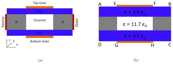
For a double-gate MOSFET [22, 83], the computational dimensions can be split into a confined direction, a transport direction and an infinite direction. Figure 1 depicts the geometric configuration and computational domain of the double-gate MOSFET. A detailed description of the involved parameters for the double-gate MOSFET is provided in section 4.1f. Along the infinite direction, the potential is assumed as translation invariant and the associated Schrödinger operator has an absolutely continuous spectrum. It can be solved with the plane waves. In the confined direction where the gate voltages are applied, the associated Schrödinger operator which includes the electrostatic potential, is essentially compact, despite that the potential may admit a finite number of point singularities. Therefore, the energy spectrum is discrete in the confined direction. The transport direction accounts for the charge carrier motion in the channel connecting the source and drain contacts. The associated Schrödinger operator also has an absolutely continuous spectrum. The corresponding scattering states can be evaluated with appropriate incoming and outgoing waves, and are subject to the potential consisting of the eigenvalues computed from the confined direction. Without the lost of generality, we denote x, y and z directions for transport, infinite and confined directions, respectively. Under this setting, the total wavefunction can be expressed as
where the index j denotes the jth eigenmode of the discrete spectrum and χky (y) = eikyy is the plane wave of given wavenumber ky. As such, the Schrödinger equation of a single electron can be split into two parts
| (13) |
| (14) |
where with Ej,kx,ky being the total energy of the system, and U(x, z) is the electrostatic potential energy satisfying the Poisson equation. The solution of Eq. (13) requires the information of U.
Figure 1.
Illustration of a double-gate MOSFET with its y-direction being infinitely long. (a) Configuration of the double-gate MOSFET; (b) Computational domain.
Note that for the double-gate MOSFET, the y direction is homogeneous, we therefore can solve the Poisson equation in two dimensions. Furthermore, on the x – z plane, due to the confinement along the z direction provided by the insulator layers, combined with the assumption that the device geometry does not change significantly along transport direction, the system yields discrete states only in the z direction. We split the wavefunction as
| (15) |
where ψj(x0; z) is the discrete eigenstate in the z direction for a given x0 label and is a scattering state in the transport direction x. The eigenvalue problem with the Dirichlet boundary condition is
| (16) |
| (17) |
where εj(x0) represents the energy of the jth discrete subband at x0. Here ∂ΩD is the boundary of the silicon layer at where the wavefunction is forced to be zero because of the confinement. Based on this formalism, one only needs to calculate the quantum transport along the x-direction. We therefore end up with a scattering problem
| (18) |
Since εj(x) varies along the x axis, it serves as the potential for the scattering problem. The superscript in the scattering wavefunction indicates that the potential is associated with the jth discrete subband. Similarly, the subband label j on Ej,kx indicates the scattering potential used in Eq. (18). From the physical point of view, the scattering energy is conserved during the scattering process. The transmission and reflection coefficients can be computed based on each given initial energy Ej,kx, which is a part of the absolute continuum spectrum.
Equation (18) can be solved in many ways, such as time dependent and time independent means. However, it is convenient to use the NEGF strategy [22] as described in Section 2.3.1, which provides not only the solution to Eq. (18), but also the desirable transport quantities.
To solve the Poisson equation for U(x, z), one needs to determine the electron density n(x, z, y) according to Eq. (4)
| (19) |
where n(r) is homogeneous in y direction. In fact, the scattering part does not need to be explicitly evaluated in the NEGF formulation. The further simplification of n(r) is discussed in Section 2.3.2.
2.2.2 Four-gate MOSFET
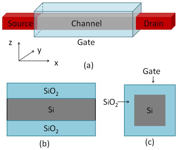
For a four-gate MOSFET, we denote x, y and z directions for the transport, confined and confined directions, respectively. In the confined y – z directions where the gate voltages are applied, the associated Schrödinger operator is essentially compact, which leads to discrete energy states for the charge carrier. Figure 2 depicts the geometric configuration and computational domain of the four-gate MOSFET. A detailed description of the four-gate MOSFET parametrs can be found in Section 4.1. As in the double-gate case, the associated Schrödinger operator has an absolutely continuous spectrum in the transport direction. The total energy is given by Ej,kx and total wavefunction is ψj,kx. By assuming , we therefore can split the Schrödinger equation as
| (20) |
| (21) |
where εj(x0) is the jth eigenvalue of the 2D problem at position x0, and ψj(x0; y, z) is the corresponding eigenfunction. Here is the scattering wavefunction associated with the scattering potential εj(x) and energy Ej,kx. The transport equation (21) is the same as that of Eq. (18) and can be solved with the NEGF method. For a given set of scattering energies, , the Poisson equation (11) is solved in 3D and its electronic density source term is
| (22) |
The further evaluation of the density is discussed in Section 2.3.2.
Figure 2.
An illustration of a four-gate MOSFET (i.e., silicon nanowire transistor). (a) Configuration; (b) Cross section at y = 0 for the computational domain; (c) Cross section at x = 0.
In both double-gate and four-gate MOSFET calculations, it is possible to consider subband interactions by using a variety of combinations of the discrete energy levels. As such, subband states belonged to different levels are used along the x axis. Obviously, this approach can lead to improved transport properties and an increase in computational cost. However, high energy modes, particularly those modes whose energies are significantly higher than the scattering barrier, do not play much role in the transport calculation.
2.3 Transport system
This section briefly describes the NEGF formalism in a setting that is consistent with the double-gate MOSFET and four-gate MOSFET studied in the present work. Additionally, a detailed description of the electron density is also given.
2.3.1 The NEGF formalism
Without the loss of generality, we consider the NEGF formalism in a multichannel setting in ℝ3−l. Here l is the number of non-scattering dimensions, it equals 2 for double-gate and four-gate MOSFETs discussed in the last subsections. We define the whole open system on the domain Ω = ΩD ∪ (∑α Ωα), which consists of the device domain ΩD and the union of (multiple) contact domains Ωα, such as the source and drain. Let Γα = ΩD ∩ Ωα denote the intersection boundaries of the device domain and contacts. Here, Ωα may extend to infinity but only the ΩD (or plus small portion of Ωα) is the computational domain of interest. In the framework of the NEGF, the Green's operator (function) on ΩD is defined as the inverse operator
| (23) |
where E is the total energy of the scattering system, I is the identity operator, H = H0 + ∑α ∑α is the full scattering Hamiltonian and H0 is the Hamiltonian of the single charge carrier associated with the scattering potential. In order to reduce the computational cost, the infinite (or large) contact domain Ωα needs to be chopped off and is restricted on the domain of interest ΩD. Each of the self-energy operators ∑α is solely defined on the corresponding Γα and reveals the coupling effect of the contacts to the device [22]. In practice, ∑α takes different forms for different numerical discretizations, and more details can be found in Ref. [49]. In the position representation
| (24) |
where m(r) is the space dependent effective mass of the charge carriers and Uscat(r) is the interaction potential for scattering and Uscat(r) = εj(x) for double-gate and four-gate MOSFETs discussed in the last subsections.
Once the Green's function/operator is defined, all quantities of interest can be calculated. Among these quantities, the scattering wavefunction is given by
| (25) |
where φE is the incoming wavefunction of energy E. The scattering wavefunction satisfies the Schrödinger equation HψE = EψE. Additionally, the non-equilibrium charge carrier density operator is given by
| (26) |
In the NEGF theory, each contact is assumed in equilibrium state and α is for contact index, μα is the contact Fermi level for each contact, and f is the Fermi-Dirac distribution. Here Hfull = H+Hns is the full Hamiltonian of the electron system with Hns being the Hamiltonian of the non-scattering system. The spectral function Aα (E) in Eq. (26) is given by
| (27) |
where Γα (E) is the broadening operator, which reflects the dissipative effects on the transport from contact region Ωα, and is defined by
| (28) |
Moreover, the number density of charge in the system is given by the position representation of the density operator (26)
| (29) |
where < ·| and |· > are Dirac notations.
Furthermore, the current in the quantum device from the source (S) to drain (D) is calculated via
| (30) |
where μS and μD are the Fermi levels of source and drain, respectively. The Tr is the trace and TDS(E) is the transmission operator
| (31) |
Finally, the number density contributed from the scattering process can also be computed by using the NEGF formalism. This aspect is elaborated in the next subsection.
2.3.2 Electron density
Electron density is an important quantity in the coupled Poisson-Schrödonger theory and is used in the Poisson equation to compute the potential. The general expression of the density is given in Eq. (29). Due to the subband decomposition, the evaluation of density becomes slightly subtle. One needs to distinguish the subband degree of freedom, the scattering degree of freedom, and the degree of freedom due to the infinity dimensions. In particular, the energy associated with infinity dimensions should be integrated. Whereas the discrete subband energies serving as the potentials for the scattering system and the discrete subband states are summed over. We illustrate the density evaluation in the double-gate MOSFET and the four-gate MOSFET.
As shown in Eq. (29), the electron density is given by the position representation of the density operator n(r)scat =< r|ρ|r >. For the double-gate MOSFET, the y direction is infinity and homogeneous. The total energy Ej,kx,ky is distributed to the plane wave, the eigenstate, and the scattering kinetic energy. Since the eigenstate energy acts as the scattering potential energy, the total energy available to the scattering system in Eq. (23) is . The energy associated with the plane wave can be integrated. To evaluate ρ, we need to use some notation and identities
| (32) |
and
| (33) |
for a function g(k). We therefore write the electron density of the double-gate MOSFET as
| (34) |
| (35) |
| (36) |
| (37) |
where . Since ky is continuous, we should change the summation into an integral
| (38) |
| (39) |
where is the Fermi integral of order given by
| (40) |
From Eq. (29), we have
| (41) |
| (42) |
From this expression one can identify that .
At each given location along the x direction, Ej,kx is given by . Based on this expression and Eq. (15), the density n(r) given in Eq. (41) can be calculated. The Schrödinger equation and the Poisson equation are completely coupled and their solutions have to be pursued iteratively.
For the four-gate MOSFET, the density can be evaluated as the follow
| (43) |
| (44) |
where is given by
| (45) |
Note that in Eqs. (42) and (45), the integrations over energy Ej,kx are carried out at each given position x.
2.4 Electrostatic system
The electrostatic system is governed by the Poisson equation. The solution of the Poisson equation, i.e., electrostatic potential, provides the potential energy landscape for the electron to scatter through according to the Schrödinger equation. However, the solution of the Poisson equation depends, in turn, the electron density, dopants, and material interfaces. This subsection discusses new doping model and interface model used in the Poisson equation.
2.4.1 Individual dopant model
Introducing appropriate impurity atoms (known as dopants) into a semiconductor provides electron reservoirs and can increase the electrical conductivity by many orders of magnitude. By doping a semiconductor device, we can engineer its electrical properties, i.e, its conductivity, electrostatic potential and its charge carrying mode. Doping is a key to our understanding of semiconductor devices and a strategy for the design and manufacture of desirable devices [41, 43, 42].
In continuum modeling, dopants have either been described as continuous distributions in p-n regions or been formulated as a change in the dielectric effect, leading to different dielectric values in different p-n regions. These treatments work mostly well for the prediction of device properties. However, when the channel length reduces to about 10 nm, the quantum effect becomes important, thus, each doping atom may have a dramatical impact to the quantum state of nearby electrons. Atomistic model for dopants becomes indispensable. Wong and Taur [97] provided a classical study of discrete random dopants. Recently, quantum random dopant models are applied to the channel of sub-0.1 μm [7] and 25nm [50] MOSFETs for threshold voltage lowering and fluctuations. The impact of random dopant aggregation in source and drain is studied via the NEGF formalism [71]. It is found in these studies that doping is only macroscopically controllable when the discrete microscopic dopant distribution is also controlled. Macroscopically, identical devices may suffer from strong performance variations because of the microscopic differences. Therefore, it is important to understand individual dopant effect in nano electronic devices.
In earlier individual models, the discrete dopants are approximated by either dilated Gaussian functions [50] or constant charges supported by small regions. All these models are parameter-dependent. In this paper, we propose a point doping model for individual dopants and define the doping density as
| (46) |
where where β = n-dopants and p-dopants, cβ are charges of doping atoms and δ(r − rjβ) is the Dirac delta function at position rjβ. Theoretically, this doping charge source can be added to the total energy functional, Eq. (10). This model provides a better description for microscopic dopants. In fact, it has a connection to the usual Gaussian function model characterized by the influence domain (σβ) of each dopant
| (47) |
The point doping model is recovered if the influence domains are set to zero. Computationally, the delta functions give rise to unbounded electrostatic values locally and is numerically difficult to deal with. This singularity can be alleviated by the Dirichlet to Neumann mapping (DNM) method, which analytically resolves the delta functions and leads to a set of flux jump conditions at the interface. The effective use of the DNM method requires the careful enforcement of additional flux jump conditions. To this end, the MIB framework developed for the Poisson equation will be used. Tens of thousands of atoms can be handled in this approach.
2.4.2 Interface modeling
Material interfaces, such as semiconductor-to-insulator interfaces, are crucial features of MOSFETs. Semiconductors with better electrical properties than silicon, such as gallium arsenide, that do not form distinct semiconductor-to-insulator interfaces, are unsuitable for MOSFETs. Typically, dielectric constants of different components in MOSFETs vary dramatically. For example, the dielectric constant of the silicon dioxide insulator is a few times smaller than that of the buck silicon substrate. The ratio of dielectric constants in different layers is also important to the device scaling. According to device scaling physics [37], the scale length Λ of the device, for the first order approximation, depends on the insulator thickness (TI) and the ratio (∊Si/∊I) of dielectric constants of the silicon and the insulator in the way
where Wdm is the maximum channel depletion depth relating to the channel doping concentration. The above theory predicts that the proper minimum design length lies between Λ and 2Λ. It is clear that smaller value of TI and larger value of ∊I help device scaling. Replacing the silicon dioxide gate dielectric with a high-k material allows increased gate capacitance without the concomitant leakage effects. The proper formation of distinct interfaces is a stringent requirement for ultimate CMOSs and functional electronic devices to suppress leakage currents due to tunneling, as the thickness scales much below 2 nm. Computationally, it is important to be able to simulate the interface roughness and irregularity due to the device fabrication processes [56]. The use of interface description is indispensable for modeling of ultimate and functional CMOSs.
The recognition of material interfaces in MOSFETs implies the acknowledgment of discontinuous material properties or coefficients across the interfaces. This has profound consequences in the well-posedness and numerical convergence of the Poisson equation. For simplicity, the electron is assumed as the majority of charge carriers and then the hole density is neglected. In the present work, we consider the Poisson equation of the form
| (48) |
| (49) |
| (50) |
where un = (∇u) < n with n being the interface normal direction, letters “A” and “D” denote acceptor and donor, respectively, and MA and MD are numbers of discrete acceptors and donors, respectively. Being a multi-scaled model, some doping regions in the device may still be modeled as continuum, and thus the continuous doping functions NA and ND are reserved for these specific parts. This treatment is reasonable. For example, when the doping in the channel is small and the system is dominated with electron ballistic transport, the continuum doping treatment is a good approximation. Another case is that when the voltage threshold lowering effect is studied, individual dopants are used for the channel region while continuum doping treatment can be used in the source and drain regions. The computational domain Ω is divided into silicon ΩSi and insulator ΩSiO2 layers. The interface is defined as ΓSi/SiO2, i. e., Ω = ΩSi ∪ ΩSiO2, ΓSi/SiO2 = ΩSi ∩ ΩSiO2. It follows that the dielectric constant ∊ is set to as ∊Si and ∊SiO2 in corresponding regions. The solution of the Poisson equation u(r) is restricted to the silicon (Si) and insulator (SiO2) regions, and denoted as uχΩSi and uχΩSiO2 respectively, where χΩ is the characteristic function on set Ω. Models (49) and (50) indicate that the Poisson equation is subject to the jump conditions along the Si/SiO2 interface, where the jump conditions reveals the continuities of the potential landscape and its flux.
Although the jump conditions are trivial in physical sense, if no specific numerical algorithm is applied, the discontinuity induced non-smoothness in the solution will be smeared. As such, the numerical scheme is of low accuracy and convergence. A novel numerical scheme, the matched interface and boundary (MIB) method will be illustrated in the next section. The boundary conditions of the Poisson equation are the following: it takes Dirichlet boundary conditions where the gate voltages are applied and Neumann boundary conditions for the rest of the device.
3 Computational algorithms
In this section, we discuss computational algorithms used in this work. We first give a brief description of the MIB method used for simulating the interface problem formulated in Section 2.4.2. Secondly, the Dirichlet-to-Neumann mapping (DNM) formalism is introduced to achieve an accurate and efficient account of randomly distributed dopants formulated in Section 2.4.1.
3.1 Matched interface and boundary (MIB) method
As stated in the previous sections, the proposed interface and individual dopant models involve elliptic equations with arbitrary interface shapes, discontinuous coefficients and singular sources. The design of numerical schemes for these problems is a challenging task in scientific computing. To achieve designed numerical convergence for elliptic equation with discontinuous coefficients and regular source term, all the continuity conditions(homogeneous jump conditions) have to be enforced at the interface. For those elliptic equations with singular source like delta functions, the singularity may be removed and the whole systems is converted to interface problem with inhomogeneous jump conditions. In the past decades, there are continuous efforts in developing mathematical techniques for this class of problems. In this work, the MIB method will be utilized to deal with these problems. There are two reasons for us to choose the MIB technique. First, as a modification of the standard finite difference (FD) scheme, the MIB achieves the second order convergence in solving the Poisson equation with interfaces and discontinuous coefficients. Additionally, the individual dopants in our model are solved analytically by using the Dirichlet-to-Neumann mapping (DNM) technique, which yields inhomogeneous jump conditions along the interface. Although the second order convergence of the overall solution may be slightly undermined by the nonlinear self-consistent iterations, as the following example shows, the MIB method still offers better accuracy than the standard FD method does. Furthermore, inhomogeneous jump conditions derived from the DNM technique must be incorporated with interface method in order to obtain the correct solution. On requirement of good accuracy and correctness in the numerical implementation of the proposed model, the MIB scheme is the most important recipe, from which more reliable results can be expected with relatively coarse grids.
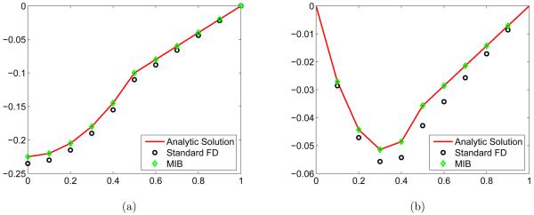
For the numerical simulation of semiconductor devices, the grid resolution can not be too high due to the computational burden. Figure 3 show a simple example on the solution accuracy of the MIB against that from the standard FD scheme. The sample problem is
| (51) |
where
| (52) |
Figure 3.
Comparison of solutions of the Poisson equation obtained by using the standard FD and the MIB methods. (a) Solutions to problem (51) with mixed boundary conditions; (b) Solutions to problem (51) with Dirichlet boundary conditions.
The graph in Fig. 3(a) is subject to the mixed boundary condition u′(0) = 0, u(1) = 0 and that in Fig. 3(b) is subject to the Dirichlet boundary condition u(0) = u(1) = 0. The example is simple but represents the profiles of the transport and confined directions in the device-related Poisson equation and the analytical solution can be easily derived. It is clear that, no matter under what boundary conditions, even at coarse grid of spacing h = 0.1, the MIB solution agrees with the analytical solution very well. Whereas the standard FD solution does not match the analytical one. Higher grid resolution, which also means more computational cost, is needed for the standard FD to obtain a similar level of accuracy. The reader is referred to Refs. [100, 108] for more details about high-order MIB schemes and their other applications.
3.2 Dirichlet-to-Neumann mapping
The proposed interface and individual dopant models (48) treat the dopants as Dirac delta functions, which poses computational difficulties. As an approximation, delta functions can be distributed to the neighboring grid points [99]. However, due to the application of the interface techniques, the interference of the interface treatment and the distributed delta functions leads to the reduction of accuracy to the first order. As such, the combination of an interface technique and a Dirichlet-to-Neumann mapping (DNM) strategy becomes necessary [40]. This combination can substantially improve computational accuracy and the speed of convergence. The essence of the DNM technique is to split the solution into certain parts, such that the singular source terms can be accounted in one part of the solution analytically. Such a treatment will in general produce an additional Neumann condition either on the interface or on the boundary.
In the present problem of nonlinear iterations, we can further take the advantage of the solution splitting to accelerate the convergence of the iterations. It is also noted that in the Poisson equation, only the electron density n(r) is directly involved in the loop of self-consistent iterations and it is a regular function. Therefore, we first decompose the solution of the Poisson equation into two parts, a slow varying part and a fast varying part: u = uslow + ufast. The fast varying part is up-dated during the iterations and solves
| (53) |
where ΓSiO2/Gate is the interface between the insulator and the metal contact. At the Si/SiO2 interface ΓSi/SiO2, Eq. (53) is subject to the jump conditions
| (54) |
| (55) |
The slow varying part uslow solves
| (56) |
subject to jump conditions
| (57> |
| (58) |
Here uslow is solely contributed from the fixed doping terms, either continuous doping or individual dopants. It is noticed that jump conditions in both (53) and (56) are decoupled. Therefore, solutions uslow and ufast are decoupled too. As such, we only need to undate ufast during the nonlinear iterations.
For a given n(r), the system (53) with its jump condition is readily to be solved with the MIB method. Whereas, uslow should be further decomposed as
where ucont and udisc are the solution associated with continuous doping and individual doping, respectively. Since there is no doping in ΩSiO2, we set u1 = ucontχΩSi + (ucont + udisc)χΩSiO2 and u2 = udiscχΩSi. Here u1 solves
| (59) |
subject to jump conditions
| (60) |
| (61) |
Similarly, u2 solves
| (62) |
subject to the jump conditions
| (63) |
| (64) |
In this manner, we have decomposed uslow into two systems (59) and (62) with corresponding boundary conditions and jump conditions (60-61) and (63-64), respectively. The boundary conditions appear trivial, following the homogeneous Dirichlet and Neumann boundary conditions from uslow. However, it can be seen that the jump conditions, specifically the flux jump conditions in Eqs. (61) and (64), have been revised. They need to be carefully evaluated.
Since u2 is zero on ΩSiO2, we can restrict u2 on ΩSi. As such, interfaces Si/SiO2 play the role of boundaries, where the homogeneous Dirichlet boundary conditions are applied, which also results in homogeneous jump conditions in Eqs. (60) and (63). However, one cannot generally have the homogeneous Dirichlet condition and the Neumann boundary condition simultaneously. The Neumann boundary of u2 on Si/SiO2 interfaces creates nonhomogeneous jump conditions in Eqs. (61) and (64), which is denoted by ϕ and is computed as the follow.
For u2 = u2χΩSi, it can be written as u2 for simplicity and it satisfies:
| (65) |
To solve equation (65), we set u2 = u* + u0, in which
| (66) |
for 2D simulation, and
| (67) |
for 3D cases. Finally, u0 solves the harmonic equation with the corresponding boundary condition
| (68) |
It follows that the jump ϕ in Eqs. (61) and (64) reads
| (69) |
Note that Eqs. (66) and (67) are actually the fundamental solutions of the Laplacian operator with the δ function source in an unbounded domain. Harmonic equation (68) is used to restrict the fundamental solution in the bounded domain and match the boundary conditions. This procedure of rendering a Neumann boundary condition on the interface from the original Dirichlet boundary condition u* is called Dirichlet-to-Neumann mapping. Meanwhile, the is used as the jump at Si/SiO2 interfaces of the flux of u2, if the whole domain Ω = ΩSi ∪ΩSiO2 is considered. It is easy to identify that the δ functions for individual dopants are exactly treated without any approximation by this decomposition of the whole problem in to sub-systems (53), (59) and (62) with corresponding boundary conditions. Other than the naturally induced homogeneous interface jump conditions, the decomposition of the problem also introduces nonhomogeneous jump conditions. Systems (53), (59) and (62) are typical interface problems and are to be solved by the MIB method.
4 Numerical implementation and device simulation
Multigate MOSFETs have become an important means to alleviate channel tunneling and gate leaking in ultimate CMOSs. In this section, we consider two multigate MOSFETs, the double-gate MOSFET and the four-gate MOSFET. The proposed interface model and individual doping model are evaluated in this section.
4.1 Device configurations
In the following sections, the proposed model and numerical implementation are used to examine the effects of random individual dopants and material interface. The impact of individual dopant random fluctuation was first recognized by Hoeneisen and Mead in 1970s and has been studied for many years via semiclassical or quantum mechanical means. Among the quantum models, Martinez et al [71] explored the impact of random dopant aggregation in the source and drain. Jiang et al [50] studied the gate threshold voltage lowering and fluctuation induced by random dopants in the channel. These studies are based on the smooth function approximation of individual dopants. The results from this treatment depend on empirical parameters and discretization mesh sizes. By using the Dirichlet-to-Neumann mapping, it can be found in the numerical simulation that the Dirac function model proposed in this work treats the individual dopants exactly, is of parameter free and does not require fine grids.
Multi-gate MOSFETs will play a dominant role in quantum devices because their ability to suppress channel tunneling and gate leaking effects. A variety of related investigations are carried out for such device models. We consider multi-gate MOSFETs in this work. Figure 1(a) gives an illustration of the 2D double-gate MOSFET and Fig. 1(b) is the corresponding computational domain. All relevant components of the device are presented in the graph. The x-direction is taken as the transport direction, the z-direction as the confined direction and all physical profiles are assumed invariant along y-direction. In the gray region, the source and drain are heavily doped while the channel is assumed near ballistic therefore no doping is imposed. It is noticed from Fig. 1 (b) that the dielectric constants are different in the silicon and silicon dioxide layers, which are separated by the interfaces. For the Poisson equation on the computational domain, Dirichlet boundary conditions are taken at the double-gate region (EF and GH). For other boundaries (AE, FB, BC, CH, DG and AD), homogeneous Neumann boundary conditions are employed. The parameters of the device are the following: The total length (AD) of the device is 30 nm, with 10nm for each doping area and channel. The thickness of the silicon layer is 3nm, while the upper and lower silicon dioxide layers are 1nm each.
Figure 2(a) is the 3D sketch of the silicon nanowire transistor (SNWT), which is a MOSFET with all-around gates. The x-direction is the transport direction, while the other two are confined directions, where insulator layers exist and gate voltages are applied. In our simulation, for simplicity, the cross-section of the SNWT is taken as square, so it is also called a four-gate MOSFET. Figure 2(b) gives the cross-section of the SNWT in the y-direction (y = 0). It is similar to the structure of the planar double-MOSFET. Figure 2(c) presents the cross-section of the SNWT in x-direction (x = 0). The total length of the device is 30 nm, with 10nm for each doping area and the channel. The thickness of the silicon layer is 3nm. The thickness of the upper and lower silicon dioxide layers is 1nm each. Treatments that are similar to those for the double-gate MOSFET are taken for the boundary condition. If the slice has gate all around it, the Dirichlet boundary condition is imposed, otherwise homogeneous Neumann boundary condition is imposed.
The strategies of placing individual dopants are as following: The discrete dopants are located for the 5nm long region right before the channel in the source contact and 5nm long region right after the channel in the drain contact. These regions are called discrete regions. The rest areas of the source/drain are self-averaging areas with continuum doping because a sufficient number of doping is necessary [71]. The number of individual dopants MD and each dopant charge quantity cj are chosen to match the self-averaging doping concentration in the sense of an integration
| (70) |
where ND(r) is the continuous doping. Individual dopants are randomly and evenly distributed in the discrete region, i.e. the x- and y-coordinates of the dopants are independently generated by a uniform quasi-random number generator.
4.2 Numerical implementation of the self-consistent iterations
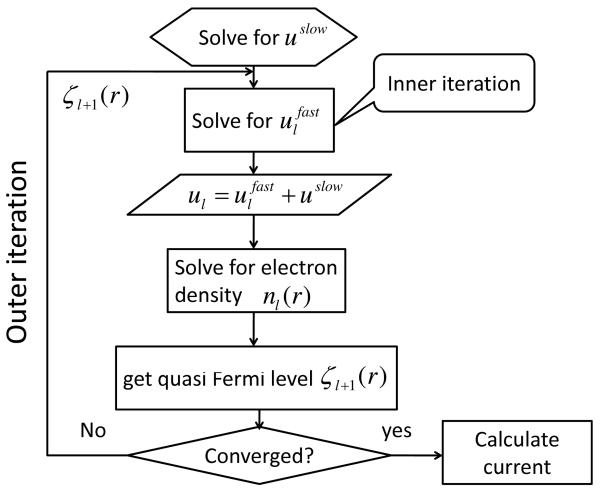
To achieve efficient convergence, we present an inner-outer iteration procedure in this section. The Gummel iterative scheme was proposed in [26] for solving nonlinear coupled equations in all kinds of device applications. The numerical implementation of the iteration scheme for the nano device simulation is provided below.
Step 0 (Solution of uslow) : This step is out of the main iteration loop to solve for uslow, which is related to the fixed discrete and continuous doping functions. u*, the singular part of uslow, is calculated by using Eq. (66) for 2D or Eq. (67) for 3D. The Harmonic part u0 is solved on the silicon region by using Eq. (68). Therefore, u* + u0 is the part of uslow from the discrete doping, and their corresponding interface jump ϕ is derived via Eq. (69). The continuous doping part, u1, is solved from via Eq. (59) and the corresponding jump condition (60). Finally one obtains uslow = u1 + u* + u0.
- Step 1 (Inner iteration for the Poisson equation): Given the quasi-Fermi level function in lth step, ζl, and the calculated uslow, solve the nonlinear Poisson equation for
where n0 is the intrinsic density-of-state of an electron system(71)
where ℱ1/2(x) is the Fermi-Dirac integral of order 1/2, which takes the form of(72)
Here, ζ(r) is the quasi-Fermi potential and will be used as an index function to determine the convergence. The initial value ζ0(r) is obtained via a linear interpolation of the source and drain Fermi levels (voltages) over the channel. This initial guess is found to be very effective in our numerical simulations.(73) - Step 2 (Inner iteration for the Schrödinger equation): The outcome of the Step 1 is the electronic potential at lth step, . Along the transport direction (say x-direction), we slice the electronic potential for each fixed x0, and solve the eigenvalue problem either in 1D for the double-gate MOSFET or in 2D for the four-gate MOSFET
where ul(r) = ul(r)(−q). Results from this step are set of and .(74) - Step 3 (Update density and quasi-Fermi potential): With the available of subband energies , we calculate the 3D electron density nl(r) by using Eq. (42) or Eq. (44) at the lth step. Once nl(r) is obtained, one can update the quasi-Fermi level to the (l + 1)th step ζl+1 by inverting the expression nl(r) = n0ℱ1/2(ζl+1(r) − ul(r))
(75) Step 4 (Convergence check): The convergence is checked by the criterion of ∥ζl+1(r) − ζl(r)∥ < ε, where ε is a given small positive number. If the inequality is satisfied, one calculates the current via Eq. (30), otherwise go to Step 1.
Figure 4 gives the work flow of the present self-consistent iteration scheme.
Figure 4.
Work flow of Gummel-like self-consistent iterations.
Remark 1: The reason of a nonlinear Poisson equation applied here is that, during the outer self-consistent iteration loop, the fluctuation of n(r) may undermine the iteration convergence, according to [93]. The use of the Fermi-Dirac integral will average or normalize this kind of fluctuations and thus lead to efficient convergence.
Remark 2: There is no analytical form for the Fermi-Dirac integral of order 1/2. Ref. [60] provides a very accurate approximation to the integral by polynomials. It is based on these approximations in this algorithm that all the related calculations are carried out.
Remark 3: Once the nonlinear Poisson equation is employed, it is noted that the initial guess for the whole self-consistent iteration is the quasi-Fermi potential ζ(r). The choice of the initial guess is based on the physical assumption that ζ(r) are constants of the voltages at the source/drain and taken as a linear interpolation of two constants along the channel. This initial guess is found to be very effective in our numerical simulations.
4.3 Analysis of the model well-posedness
For simplicity, the present analysis is based on the double-gate MOSFET. The analysis of the four-gate MOSFET is similar. The parameters of the device are the following: The source and drain voltage bias is VDS = 0.4V, the double gate voltage is VG = 0.4V. Three subbands are accounted for electron density calculations. In the double-gate MOSFET simulation, the electron effective mass is taken as mx = 0.50m0 in the transport direction and as mz = 0.20m0 in the confined direction. The dielectric constants for silicon layer and silicon dioxide layer are ∊Si = 11.7∊0 and ∊SiO2 = 3.9∊0, respectively, where ∊0 = 8.85 × 10⁻¹²Fm−1. The reference continuous n-doping is taken as ND(r) = 2 × 10²⁰/cm3 in the source and drain. For individual dopants in channel tests, the p-doping is take as NA(r) = −1 × 10²⁰/cm3. Room temperature of T = 300K is assumed.
The well-posedness of the numerical implementation consists of the analysis of the outer iteration loop and inner solution of the nonlinear Poisson equation. We define the Ks, Us and Ns as the spaces to which the quasi-Fermi functions ζ(r), electrostatic function u(r), and electron density n(r) belong, respectively. For the whole self-consistent Poisson-NEGF system, it can be interpreted as the application of the fixed point map 𝒯 : Ks → Ks to the quasi-Fermi potential function
| (76) |
To characterize the details of the map 𝒯 : Ks → Ks, we have the operator ℒ : Ks → Us, which indicate the action of the inner iteration (71) from the quasi-Fermi potential to the system potential landscape. Then it is followed by 𝒢 : Us → Ns, the procedure of using the NEGF scheme and subband decomposition to calculate the electron density from potential. Finally the map represents the step that recovers the new quasi-Fermi level from the obtained electron density. The composition of the actions of the above operators yields the definition of the operator 𝒯, representing the outer iteration
| (77) |
We define a closed convex set
| (78) |
where C1 and C2 are lower and upper bounds of ζ in Ω. By analyzing the continuities of these operators and assuming the continuous selection hypothesis, one can prove the existence of the fixed point of the map 𝒯 by the Schauder fixed point theorem [27].
Another way to check the existence of the solution is the equivalence of the problem with the Poisson-Schrödinger system [82]. The existence of the Poisson-Schrödinger system is proved in [81] and the solution is unique with the constraint of the positivity of carrier concentration.
For the nonlinear Poisson equation, the approximation of the Fermi-Dirac integral has no stronger nonlinearity than the polynomial of order 2 [60]. In this approximation, writing the equation in a variational form, standardly checking the Palais-Smale condition and applying the Soblov embedding theorem, one can easily get the well-posedness analysis.
During the numerical implementation, the Newton-Raphson method guaranteed the convergence of the inner iteration, by picking a reasonable quasi-Fermi level. For the outer iteration, the nonlinearity is too complicated to analyze and no specific analyzing scheme has been designed so far. Many simple potential-density self-consistent loops are employed and proved numerically efficient in many engineering applications. In our model, the convergence of the scheme needs to be re-examined since the introduction of the interface and delta function in the Poisson equation significantly reduce the regularity of the solution.
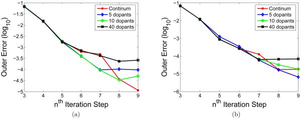
Figure 5 records the outer loop iteration of the system. The left one lists the situation when discrete dopants occur in source and drain ends, and the right one is for individual dopants in the channel. Results for a different number of dopants are compared to the continuous doping model. The horizontal axis is for the iteration loop steps. The first two steps are considered as starting steps and therefore skipped. The vertical axis is the log10 of the absolute convergence error of the potential. Generally, one can conclude that the convergence pattern of the individual dopants model follows that of the continuous model. It is found that the convergence is slight better for the situation that there are dopants in the channel, the reason might be that the gate voltage is applied on the channel part. The δ functions cause high variation of the potential landscape and Dirichlet boundary condition gives stronger suppress to these potential variations than the Neumann boundary condition does.
Figure 5.
Computational errors in simulating a double-gate MOSFET. (a) Individual doping in the source and drain with the dopant distribution shown in the lower panel of Fig. 6(a); (b) Individual doping in the channel.
In our numerical experiments, it is also noticed that for certain number of randomly located dopants, some specific dopant configurations fail the simple self-consistent outer iteration loop. The reason of the convergence failure, although not completely clear, might be the relative positions of the discrete dopants. Locally crowded individual dopants may lead to local significant variation of the potential landscape and undermine the convergence efficiency. Although the map (76) issues a fixed point, it promises no contraction property. Therefore the usually used outer iteration
| (79) |
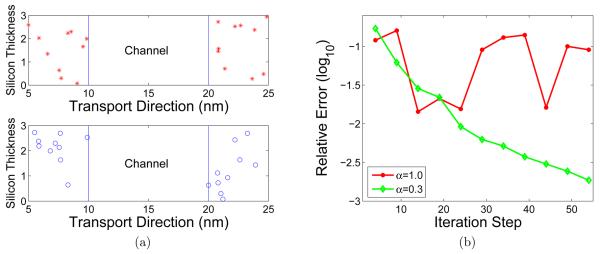
may not converge. It is difficult to verify the contraction or construct contract mapping based on these operators because of the complex nonlinearity of the NEGF calculation 𝒢. Figure 6(a) reveals these situations: The upper panel is one of the position distribution of 10 dopants that one can easily reach the steady state. The convergence behavior of the position configuration in upper panel of Fig. 6(a) can be found in Fig. 5(a). However, the distribution in the lower panel of Fig. 6(a) may lead to convergence failures. It can be seen that in the lower panel, dopants are very crowdedly distributed near the left top corner in the source. To deal with this numerical difficulty, we convert Eq. (79) into the steady-state problem of an ordinary differential equation (ODE) [5]
| (80) |
Therefore many ODE related techniques such as the Runge-Kutta method can be used to improve the convergence properties. One simple treatment is the discretization of Eq. (80) as
| (81) |
which leads to a self-consistent iteration with a relaxation factor α
| (82) |
The traditionally used outer loop iteration actually is the special case of Eq. (82) with α = 1. By carefully choosing the relax factor α, one can reach the steady state (fix point) by the self-consistent iteration for arbitrarily distributed individual dopants.
Figure 6.
Dopant distributions and iteration errors for the double-gate MOSFET. (a) Two distributions of 10 dopants. The distribution in the lower panel may lead to a divergence in the iteration. While the distribution in the upper panel leads to convergence; (b) Relaxation-factor-dependent convergence behaviors for the dopant distribution shown in the left-lower panel.
Figure 6(b) compares the convergence of the self-consistent iterations with different relaxation factors corresponding to the situation in the upper panel of Fig. 6(a). It indicates that α = 1 does not work for the convergence loop, while α = 0.3 leads to the convergence of the electron current within 0.2% relative error in around 50 steps.
One can easily come to the conclusion that although smaller relaxation factors promise the convergence, they result in more iteration steps. The exact reason of the position-dependent convergence and the choice of the optimal relaxation factor need to be further analyzed in the future.
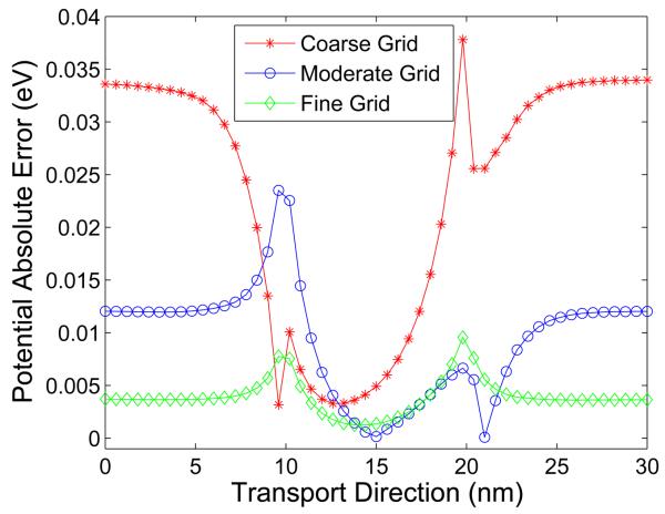
The numerical solutions of the system are supposed to converge to the real solutions as meshing grids get smaller and smaller. The standard finite difference method is of second order convergence for the inner iteration. However, the strong outer nonlinearity may ruin this theoretical rate. Moreover, the discontinuity of the dielectric constant and δ source function singularities in the Poisson equation further reduce the regularity of the solution. The standard FD method will not maintain its second order convergence. It may even diverge. The MIB scheme is designed not only for facilitating the Dirichlet-to-Neumann mapping but also for maintaining the high order convergence in interface problems. For the following convergence analysis, the numerical result obtained with a fine resolution of hx = 0.075nm, hz = 0.025nm is considered as a reference solution, where hx and hz are for the grid step along the transport and confined direction, respectively. Three sets of mesh sizes of (hx, hz) =(0.15nm, 0.05nm), (0.3nm, 0.1nm), and (0.6nm,0.2nm) are denoted as fine, moderate and coarse, respectively.
Figure 7 gives the errors under different grids resolutions in the central line of the silicon layer. Numerical results suggest the convergence of the present MIB method.
Figure 7.
Errors of simulating the double-gate MOSFET in the line of y = 0 and z = 0.
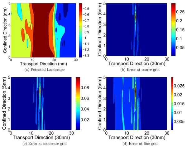
Furthermore, we examine the 2D errors of the simulation. Figure 8 presents the 2D errors for the situation when the dopant number is 10 in both the source and the drain. Combined with Figs. 7 and 8, one can conclude that the major convergent errors occur at the junctions of discrete and continuous doping regions. Errors decrease as the grid is refined.
Figure 8.
Contour plot of the electrostatic potential (a) and its absolute errors obtained with three sets of meshes(b, c, d) (10 dopants).
Finally, the L∞ norm error (Eh) is considered and the convergence order is defined as log2(Eh/Eh/2) for three sets of meshes. The numerical convergence orders are calculated for several cases with different dopants numbers and listed in Table 1. The targeted second order of the MIB method is not achieved, partially because the strong nonlinearity of the coupled equation system.
Table 1.
Computational error of the model with MIB scheme
| 5 dopants | L∞ error | order | 10 dopants | L∞ error | order | 40 dopants | L∞ error | order |
|---|---|---|---|---|---|---|---|---|
| Coarse | 0.3504 | - | Coarse | 0.3010 | - | Coarse | 0.2183 | - |
| Moderate | 0.2221 | 0.7 | Moderate | 0.1230 | 1.3 | Moderate | 0.1338 | 0.7 |
| Fine | 0.0892 | 1.3 | Fine | 0.0381 | 1.7 | Fine | 0.0475 | 1.5 |
4.4 Numerical simulation of the double-gate MOSFET
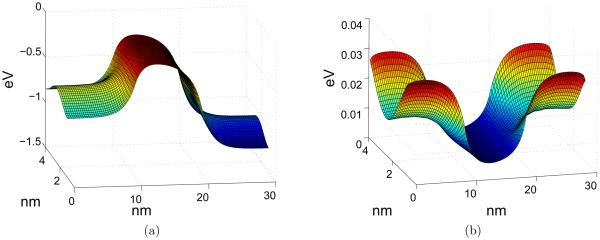
In this section, we investiagte the impact of the proposed interface model and the random individual doping model using the double-gate MOSFET. Before proceeding to the numerical results of the discrete dopant model, we show in Fig. 9(a) the landscape of the device electrostatic potential calculated from the standard finite difference method without the interface technique. The difference of the electrostatic potentials between obtained from the standard finite difference method and from the MIB method is plotted in Fig. 9(b). It is seen that two methods have about 3-4% of differences. The larest difference occurs around the interface region near insulator layers. Based on the evidence in Section 3.1, we believe that the MIB scheme gives a more accurate calculation of potential landscape. Although the advantage of the MIB scheme over the standard FD scheme is not that tremendous in this case because of the relatively simple interface geometry, the MIB technique also has the ability of handling more complex interfaces which may occur in the future MOSFET design. Additionally, the DNM treatment of the discrete dopants can not be realized without the MIB scheme.
Figure 9.
Electrostatic potential energy and difference of potentials for the double-gate MOSFET. (a) Potential landscape obtained with the standard finite difference method; (b) Difference of electrostatic potentials between computed with the standard finite difference method and with the MIB method.
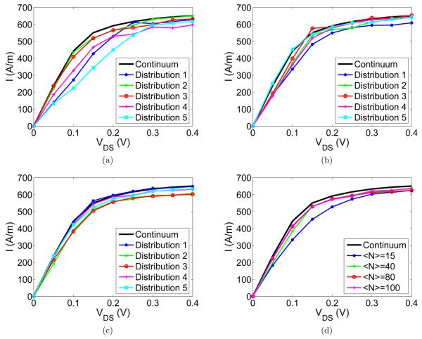
We next study the physical profiles of fluctuations under different amount of dopants and positions. The individual dopants in source or drain are anticipated to produce discrete aggregation effects: The on-state current fluctuates due to individual dopants and their relative positions. The fluctuations are not directly caused by the spatially resolved individual dopant atoms but mesoscopically by the self-consistent electrostatic potential. Physical parameters are taken as stated in the previous section. To validate the individual dopant model, we employ the constraint of Eq. (70). This constraint may appear unphysical. However, it is useful in verifying the validity of the present model. It is expected that simulation profiles of discrete dopants will converge to those of the continuous doping when the number of dopants is large. The reason is that as the number of dopants increases, the amplitude of each dopant becomes smaller and the doping becomes evenly distributed.
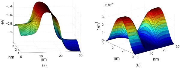
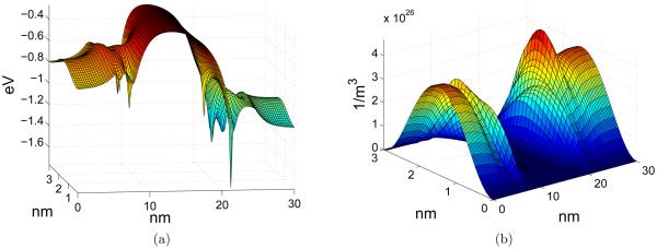
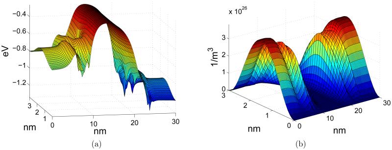
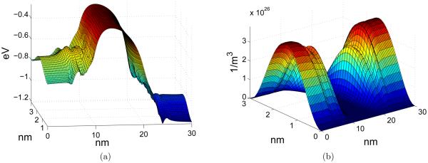
For a comparison, Fig. 10 illustrates the steady-state potential and electron density obtained using the continuum doping approximation. It is predictable that the presence of the individual dopants will drag down the potential landscape and therefore trap the electron where a discrete dopant presents. This fact is revealed in our simulations: if there were no individual dopants in the region 5-10nm and 20-25nm along the x-direction, the potential landscape and electron density there would be similar to those in the channel (10-20nm in the transport direction). Due to the presence of discrete dopants, the potential landscape is dragged down and becomes flat, as that presented in the continuous doping region (0-5nm or 25-30nm in the transport direction). As a consequence, the electron probability distribution (density) is increased near the discrete dopant site, comparing to the distribution profile of the continuous regions. Figures 11, 12 and 13 depict the potential landscapes and electron densities obtained with 5, 10 and 40 discrete dopants, respectively. Furthermore, it is observed that the more individual dopants presented in the field, the smoother the potential is, and the closer to the continuum doping model the present discrete doping will be. This is consistent with our expectation.
Figure 10.
Profiles of electrostatic potential and electron density obtained with the continuous doping approximation. (a) Potential function; (b) Electron density.
Figure 11.
Profiles of electrostatic potential energy and electron density obtained with 5 individual dopants (N = 5). (a) Potential function; (b) Electron density.
Figure 12.
Profiles of electrostatic potential energy and electron density obtained with 10 individual dopants (N = 10). (a) Potential function; (b) Electron density.
Figure 13.
Profiles of electrostatic potential energy and electron density obtained with 40 individual dopants (N = 40). (a) Potential function; (b) Electron density.
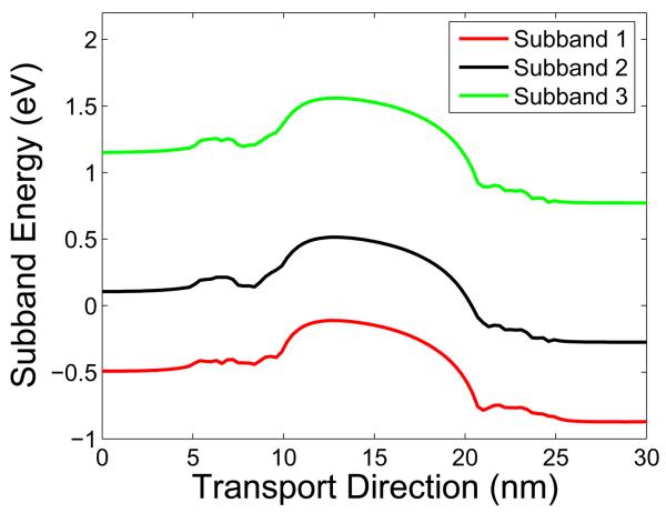
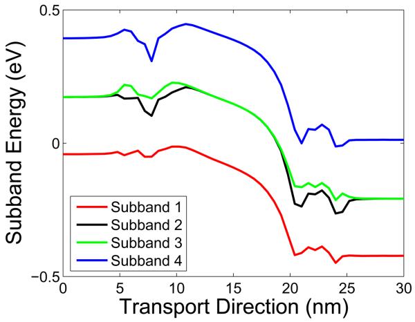
Detailed physical profiles of the device can be demonstrated by the subband energy. Figure 14 provides one of the subband energy profiles of the double-gate MOSFET with discrete dopants in the source and drain. The electron density is calculated based on the first three subband energies. Due to the Fermi-Dirac distribution, the higher the subband is, the less it contributes to the total amount of the electron density. From the subband energies profiles one can also find the flatting out effect of the individual dopants to the potential in the discrete region. Different from the continuous doping, the ‘flatting’ is oscillatory.
Figure 14.
Subband energies of the double-gate MOSFET obtained with individual dopant model.
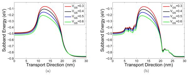
Figure 15 illustrates the first subband energy profiles of the double-gate MOSFET at different gate voltages. The increase in the gate voltage will push down the potential barrier in the device channel and thus lead to larger charge current. In this study the source/drain bias is fixed under 0.4V.
Figure 15.
Subband energy profiles under different gate voltage biases. (a) Continuum dopant; (b) Discrete dopants (10).
Figure 16 shows the first subband energy of the double-gate MOSFET under different source/drain voltage biases. The differences in the subband profiles at two ends reflect the voltage biases. The width of potential barrier is reduced when the voltage bias is increased. The increase of the voltage bias leads to the increase of charge current in the double-gate MOSFET. The gate voltage is fixed at 0.4V in this study.
Figure 16.
Subband energy profiles under different source/drain voltage biases. (a) Continuum Dopant; (b) Discrete Dopants (10).
Macroscopically, the individual dopants introduce the fluctuation in on-state currents. Figures 17(a), (b) and (c) demonstrate the current fluctuations with 5, 10 and 40 dopants, respectively. It can be observed that the fluctuation is about 10% when there are 5 dopants in different positions. The fluctuation decreases gradually when there are more dopants. From Fig. 17(d), one can draw the conclusion that the fluctuation is small when there is a large number of discrete dopants with small charge amplitude, as expected.
Figure 17.
The dependence of I-V profiles on the number of individual dopants. (a) Fluctuation of 5 dopants; (b) Fluctuation of 10 dopants; (c) Fluctuation of 40 dopants; (d) Fluctuation of different number of dopants.
Another interesting aspect of the individual dopants is the lowering effect of the device voltage threshold.
The voltage threshold of a MOSFET is defined as the gate voltage applied in order to generate the inversion layer between the insulator layer and the silicon layer, then electron current follows. The presence of the atomistic, or individual dopants has an effect of lowering the voltage threshold. In order to check the ability of our model to detect this effect, we introduce the p-type doping to the equivalent concentration of −2×10¹⁹/cm3 in the channel and compare the I-V curves obtained form the continuous model and individual dopants model.
To obtain the I-V curve presented in Fig. 18, we set the source/drain voltage biases as 0.2V (left) and 0.4V (right), and gradually increase the gate voltage from 0 to 0.4V. It is clear from Fig. 18 that, to attain the same amount current, the present individual dopants model requires less amount of gate voltage than the continuous model does. State differently, the same gate voltage gives a higher charge current in the present individual model than that in the continuous model. This fact reveals the individual dopant induced voltage threshold lowering effect.
Figure 18.
The comparison of I-V profiles under different doping models revealing the individual dopant induced voltage threshold lowering effect. (a) VS/D = 0.2V; (b) VS/D = 0.4V.
It is noted that without using the constraint of Eq. (70), the impact of individual dopants and impurity can be very significant for small nano devices. The proposed Dirac delta function model can be used for the further investigation of this aspect.
4.5 Numerical simulation of the four-gate MOSFET
In order to achieve good device performance, more effective gate control strategy is required for nano-scale MOSFETs. In this section, the four-gate MOSFET, one kind of silicon nanowire transistors (SNWTs) which resemble multi-gate or gate-all-around devices, is explored. The transport profile of an electron in the SNWT is similar to that of the double-gate MOSFET and is simulated via the NEGF as well. While being different from the planar double-gate MOSFET, the charge and potential profiles in the transverse direction are no longer invariant. 3D simulations of the SNWT with discrete dopants are implemented in this section by using the technique of the subband decomposition. The MIB method and the Dirichlet-to-Neumann mapping in 3D versions described in the previous sections are employed. The configuration of the SNWT is given in Fig. 2 and the detailed parameters are almost the same as those in the double-gate MOSFET, except that the y-direction width is 5nm, with 3nm for the silicon layer and 1nm for each SiO2 layer. The effective mass in the y-direction is taken as mz = 0.318m0.
The main difference of the present simulation and the simulation of the double-gate MOSFET is that one needs to solve the Schrödinger eigenvalue problem in 2D for each slice of the device. Additionally, the Green's formula for δ– functions takes a different form, as discussed in an earlier section.
Main results from simulating the four-gate MOSFET are quite similar to those of simulating the double-gate MOSFET. For example, the relation between the subband energy and S/D bias (or gate voltage) are generally similar to those of the double-gate MOSFET. Figure 19 shows the first 4 subband energies of the SNWT with 15 discrete dopants in source and drain under 0.4V S/D bias and gate voltages. Because a 2D eigenvalue problem is solved, the second and third subbands are almost identical (they are identical for continuous dopants). The fourth and fifth subbands are very similar too. Only the fourth subband is plotted.
Figure 19.
Subband energies for the four-gate MOSFET. The dopants break the symmetry and energy degeneracy in the second and third subbands.
Figure 20 presents the potential profile in the four-gate MOSFET at certain slice in the source region. It is found from Fig. 20(a) that the profile is symmetric due to the uniform doping and the symmetry of the device. While due to the presence of the randomly distributed individual dopants, the potential profile is no longer symmetric.
Figure 20.
Cross-section of potential profiles for the four-gate MOSFET obtained with (a) Continuum doping; (b) Discrete dopants (10).
Finally, as in the last section, the current fluctuation of the four-gate MOSFET with individual dopants is studied and the I-V characteristics is presented in Fig. 21. For comparison to previous section, the current is re-scaled to current density according to the device geometry. Figures 21 (a), (b) and (c) are I-V curves of the SNWT with 15, 40 and 80 dopants in different positions, respectively. While Fig. 21(d) shows the fluctuations with different numbers of dopants. For each number of dopants, the current values are averaged out with different positions. It can be concluded that as the number of individual dopants increases, the I-V curve is getting closer to the profile of the continuous doping. This verifies the validity of our modeling for the same reason stated in the last section.
Figure 21.
Current fluctuations of the four-gate MOSFET with (a) 15 dopants; (b) 40 dopants; (c) 80 dopants; (d) Different number of dopants.
5 Concluding remarks
This paper presents mathematical modeling and computational algorithms to nano-scale electronic devices, or ultimate metal oxide semiconductor field effect transistors (MOSFETs). MOSFETs are the elementary building blocks of integrated circuits, such as microcircuits, microchips, or silicon chips, which are used in almost all electronic devices or equipments presently in use and have revolutionized the world of electronics in the past few decades. For years, MOSFETs are designed and functioning according to classical mechanical laws. The continuous miniaturization of nano transistors has led to a new era in design, manufacture, modeling and simulation of nano electronic devices where the quantum effects start to play a very important role. The benefits from the success of these new devices can be tremendous: On one hand, the new generation of ultimate MOSFETs will dramatically advance current semiconductor technology and still operate with the classical principle after suppressing severe quantum effects. On the other hand, functionally enhanced MOSFETs, or nano-quantum transistors, that utilize the fundamental properties of nature which do not have direct analogs in classical physics, will lead to new breakthroughs in device science and technology. However, enormous degrees of freedom of nano electronic devices make their first principle quantum mechanical modeling and simulation essentially intractable. Efficient mathematical modeling, approximation, and computation for this class of problems promise an important topic in applied and computational mathematics. This work addresses a few important issues in the modeling and simulation of nano electronic devices.
A simple and perhaps the most popular model is the effective mass description of a single electron in band structures governed by the Schrödinger equation with an electrostatic potential solved from the Poisson equation. Even at this level of description, current modeling and simulation hardly take into account the significant impact of individual dopants, irregular geometric designs and material interfaces, due to the complexity and challenge of the problem. Additionally, inconsistence in many approximations undermines their performance. The present work addresses the above mentioned problems. First, we introduce a two-scale variational framework that, upon energy optimization, generates new self-consistently coupled Poisson-Kohn-Sham equations, or Poisson-Schrödinger equations. In this framework, the quantum dynamics of microscopic particles is determined by a nano-scale environment, which models the continuum electrostatics governed by the classical Maxwell's equation. As such, classical theory and quantum mechanics are put in an equal footing at nano-scale. Additionally, the magic and art of semiconductors are, by and large, due to the manipulation of layered structures. Such structures have great impact in electrostatic potentials and thus, electronic properties. In this work, we introduce material interfaces in coupled Poisson-Schrödinger equations to properly describe the interface effect to the electrostatic potential. Finally, random dopants and impurity have a dramatical impact to the electronic structures and electronic transport. We present a new individual dopant model by utilizing the Dirac delta function. Unlike previous individual dopant models [97, 7, 71, 50] that depend on tunable parameters, the proposed model is free of computational parameters.
This work also introduces two computational algorithms for the simulation of nano electronic devices. An efficient elliptic interface method, the matched interface and boundary (MIB) method [104, 108, 107, 101, 100], is employed for solving the Poisson equation with semiconductor interfaces. Although the MIB method is of arbitrarily high-order accuracy in principle, we only utilize the second order MIB scheme in the present work. However, due to the strong nonlinearity of the coupled Poisson-Schrödinger equations, the numerical order was found to be about 1.5 in the present Gummel-like iteration. The other computational algorithm employed in the present work is the Dirichlet to Neumann mapping (DNM). This approach provides a rigorous treatment of the singular charges sources in the Poisson equation due to the individual dopant model proposed in the present work. The basic idea of the DNM is to separate the singular part of the solution from the regular part, and then solve the singular part analytically. The analytical treatment of the singular part gives rise to a Neumann interface condition or boundary condition for the regular part of the Poisson equation. By splitting the Poisson equation, we have taken the advantage that the amplitudes of the both discrete dopants and continuum doping are fixed, while those of the electronic density is changing during the Gummel-like iteration. The DNM technique works well in the present device simulation.
Two multi-gate MOSFET systems, a double-gate MOSFET and a four-gate MOSFET, are considered in the numerical simulations of the present work. Both problems are modeled in the three-dimensional (3D) setting. The subband decomposition approach is utilized to simplify the computation of the electronic structures. The non-equilibrium Green's functions (NEGF) formalism is employed for the description of electronic transport. The convergence and well-posedness of the present models are analyzed. A relaxation technique is developed to improve the convergence of the iteration scheme which is subject to possible numerical divergence induced by the charge aggregation of randomly distributed individual dopants. In our double-gate MOSFET simulations, the basic characteristics and the quantum effect of the I-V curves are similar to those in the literature. The impact of randomly distributed individual dopants to electronic structure and transport is studied. In particular, individual dopant induced voltage threshold lowering effect is clearly demonstrated. In our fourgate MOSFET simulations, individual dopants effectively break the symmetry of the device. Due to the 2D quantum confinement, the density of quantum states that are relevant to the electronic transport become larger than that of the double-gate MOSFET. Effects of multigate voltage settings and irregular device geometry are under our investigation.
Acknowledgments
This work was supported in part by NSF grants DMS-0616704 and CCF-0936830, and NIH grants CA-127189 and GM-090208.
Footnotes
Publisher's Disclaimer: This is a PDF file of an unedited manuscript that has been accepted for publication. As a service to our customers we are providing this early version of the manuscript. The manuscript will undergo copyediting, typesetting, and review of the resulting proof before it is published in its final citable form. Please note that during the production process errors may be discovered which could affect the content, and all legal disclaimers that apply to the journal pertain.
Literature cited
- 1.Adams L, Li ZL. The immersed interface/multigrid methods for interface problems. SIAM J. Sci. Comput. 2002;24:463–479. [Google Scholar]
- 2.Ahmed SS, Ringhofer C, Vasileska D. Parameter-free effective potential method for use in particle-based device simulations. IEEE Tran. Nanotech. 2008;4:456–471. [Google Scholar]
- 3.Ahmend S, Vasileska D. Modelling of narrow-width soi devices. Semicond. Sci. Technol. 2004;19:S131–133. [Google Scholar]
- 4.Ancona MG, Iafrate GJ. Quantum correction to the equation of state of an electron gas in a semiconductor. Physical Review B. 1989;39:9536–9540. doi: 10.1103/physrevb.39.9536. [DOI] [PubMed] [Google Scholar]
- 5.Anderson CR. Efficient solution of the schrödinger-poisson equations in layered semiconductor devices. J. Comput. Phys. 2009;228:4745–4756. [Google Scholar]
- 6.Andrei P, Mayergoyz I. Analysis of fluctuations in semiconductor devices through self-consistent poisson-schrodinger computations. J. Applied Physics. 2004;96:2071–2079. [Google Scholar]
- 7.Asenov A. Random dopant induced threshold voltage lowering and fluctuations in sub-0.1 μm mosfet: A 3-d ‘atomistic’ simulation study. IEEE TRansactions on Electron Devices. 1998;45:2505–2513. [Google Scholar]
- 8.Ayyadi AE, Jüngel A. Semiconductor simulations using a coulped quantum drift-diffusion schrödinger-poisson model. SIAM J. Appl. Math. 2005;66:544–572. [Google Scholar]
- 9.Babuška I. The finite element method for elliptic equations with discontinuous coefficients. Computing. 1970;5:207–213. [Google Scholar]
- 10.Barraud S. Quantization effects on the phonon-limited electron mobility in ultrathin soi, ssoi and geoi devices. Semiconductor Scienec and Technology. 2007;22:413–417. [Google Scholar]
- 11.Bednarek S, Szafran B, Adamowski J. Solution of the poisson-schrodinger problem for a single-electron transistor. Zeitschrift fur Angewandte Mathematik und Physik. 2000;61:4461–4464. [Google Scholar]
- 12.Ben Abdallah N, Mouis M, Negulescu C. An accelerated algorithm for 2d simulations of the quantum ballistic transport in nanoscale mosfets. J. Comput. Phys. 2007;225:74–99. [Google Scholar]
- 13.Borli H, Kolberg S, Fjeldly TA, Iniguez B. Precise modeling framework for short-channel double-gate and gate-all-around mosfets. IEEE T Electron Devices. 2008;55:2678–2686. [Google Scholar]
- 14.Bramble J, King J. A finite element method for interface problems in domains with smooth boundaries and interfaces. Adv. Comput. Math. 1996;6:109–138. [Google Scholar]
- 15.Bufler FM, Schenk A, Fichtner W. Efficient monte carlo device modeling. IEEE T Electron Devices. 2000;47:1891–1897. [Google Scholar]
- 16.Cai W, Deng SZ. An upwinding embedded boundary method for maxwell's equations in media with material interfaces: 2d case. J. Comput. Phys. 2003;190:159–183. [Google Scholar]
- 17.Caughey DM, Thomas RE. Carrier mobilities in silicon empirically related to doping and field. IEEE Proc. 1967;55:2192–2193. [Google Scholar]
- 18.Chen D, Wei GW, Cong X, Wang G. Computational methods for optical molecular imaging. Communications in Numerical Methods in Engineering. doi: 10.1002/cnm.1164. in press. [DOI] [PMC free article] [PubMed] [Google Scholar]
- 19.Cheng Y, Gamba IM, Majorana A, Shu C-W. A discontinuous galerkin solver for boltzmannpoisson systems in nano devices. Computer Methods in Applied Mechanics and Engineering. 2009;198:3130–3150. [Google Scholar]
- 20.Cui Y, Zhong Z, Wang D, Wang WU, Lieber CM. High performance silicon nanowire field effect transistors. Nano Letters. 2003;3:149–152. [Google Scholar]
- 21.Curatola G, Doornbos G, Loo J, Ponomarev YV, Iannaccone G. Detailed modeling of sub-100-nm mosfets based on schrodinger dd per subband and experiments and evaluation of the performance gap to ballistic transport. IEEE Trans. Electron Devices. 2005;52:1851–1858. [Google Scholar]
- 22.Datta S. Nanoscale device modeling: the green's function method. Superlattices and Microstructures. 2000;28:253–278. [Google Scholar]
- 23.Datta S. Electronic Transport in Mesoscopic Systems. Cambridge University Press; 1995. [Google Scholar]
- 24.de Falco C, Gatti E, Lcacaita AL, Sacco R. Quantum-corrected drift-diffusion models for transport in semiconductor devices. J. Comput. Phys. 2005;204:533–561. [Google Scholar]
- 25.de Falco C, Jerome JW, Sacco R. A coupled schrödinger drift-diffusion model for quantum semiconductor devices simulations. J. Comput. Phys. 1964;181:222–259. [Google Scholar]
- 26.de Falco C, Jerome JW, Sacco R. A self-consitent iterative scheme for the one-dimensional steady-state transistor calculations. IEEE Trans. Ele. Dev. 1964;11:455–465. [Google Scholar]
- 27.de Falco C, Jerome JW, Sacco R. Quantum-corrected drift-diffusion models: Solution fixed point map and finite element approximation. J. Comput. Phys. 2009;204:533–561. [Google Scholar]
- 28.Degond P, Gallego S, Mehats F. An entropic quantum drift-diffusion model for electron transport in resonant tunneling diodes. J. Comput. Phys. 2007;221:226–249. [Google Scholar]
- 29.Doyle BS, Datta S, Doczy M, Hareland S, Kavalieros BJ, Linton T, Murthy A, Rios R, Chau R. High performance fully-depleted tri-gate cmos transistors. IEEE Trans. Electron Devices. 2003;24:263–265. [Google Scholar]
- 30.Duan XF, Huang Y, Ciu Y, Wang JF, Lieber CM. Indium phosphide nanowires as building blocks for nanoscale electronic and optoelectronics devices. Nature. 2001;409:66–69. doi: 10.1038/35051047. [DOI] [PubMed] [Google Scholar]
- 31.Fedkiw RP, Aslam T, Merriman B, Osher S. A non-oscillatory Eulerian approach to interfaces in multimaterial flows (the ghost fluid method) J. Comput. Phys. 1999;152:457–492. [Google Scholar]
- 32.Ferrier M, Clerc R, Ghibaudo G, Boeuf F, Skotnicki T. Analytical model for quantization on strained and unstrained bulk nmosfet and its impact on quasi-ballistic current. Solid-State Electrons. 2006;50:69–77. [Google Scholar]
- 33.Fiori G, Di Pascoli S, Lannaccone G. Three-dimensional simulations of quantum confinement and random dopants effects in nanoscale nmosfets. J. Comput. Theor. nanoscience. 2008;5:1115–1119. [Google Scholar]
- 34.Fiori G, Lannaccone G. Three-dimensional simulation of one-dimensional transport in silicon nanowire transistors. IEEE T Nanotechnology. 2007;6:524–529. [Google Scholar]
- 35.Fischetti MV. Master-equation approach to the study of electronic transport in small semiconductor devices. Phys. Rev. B. 1999;59:4901–4917. [Google Scholar]
- 36.Fixel DA, Hitchon WNG. Convective scheme solution of the boltzmann transport equation for nanoscale semiconductor devices. J. Comput. Phys. 2007;227:1387–1410. [Google Scholar]
- 37.Frank DJ, Taur Y, Wong HSP. Generalized scale length for two-dimensional effects in mosfets. IEEE Electron Dev. Lett. 1998;10:385–387. [Google Scholar]
- 38.Galler M, Schurrer F. A deterministic solver for the transport of the algan/gan 2d electron gas including hot-phonon and degeneracy effects. Jounal of Computational Physics. 2005;210:519–534. [Google Scholar]
- 39.Galler M, Schurrer F. Mathematical properties of a kinetic transport model for carriers and phonons in semiconductors. Zeitschrift fur Angewandte Mathematik und Physik. 2007;58:907–925. [Google Scholar]
- 40.Geng W, Yu S, Wei GW. Treatment of charge singularities in implicit solvent models. Journal of Physical Chemistry. 2007;127:114106. doi: 10.1063/1.2768064. [DOI] [PubMed] [Google Scholar]
- 41.Gross W, Vasileska D, Ferry D. A novel approach for introducing the electron-electron and electron-impurity interations in partical-based simulations. IEEE Electron Device Letters. 1999;20(9):463–465. [Google Scholar]
- 42.Gross W, Vasileska D, Ferry D. Three-dimensional simulations of ultrasmall metal-oxide-semiconductor field-effect transistors: The role of the discrete impurities on the device terminal characteristics. Journal of Applied Physics. 2002;91(6):3737–3740. [Google Scholar]
- 43.Gross WJ, Vasileska D, Ferry DK. Ultrasmall mosfets: The importance of the full coulomb interaction on device characteristics. IEEE Transactions on Electron Devices. 2000;47(10):1831–1837. [Google Scholar]
- 44.Han ZY, Goldsman N, Lin CK. Incorporation of quantum corrections to semiclassical two-dimensional device modeling with the wigner-boltzmann equation. Solid-State Electronics. 2005;49:145–154. [Google Scholar]
- 45.Harbola U, Mukamel S. Superoperator nonequilibrium green's function theory of many-body systems; applications to charge transfer and transport in open junctions. Physics Report - Review Section of Physics Letters. 2008;465:191–222. [Google Scholar]
- 46.Hohenberg P, Kohn W. Ihnomogeneous electron gas. Phys. Rev. 1964;136:B864B871. [Google Scholar]
- 47.Hu H, Lu ZY, Elstner M, Hermans J, Yang WT. Simulating water with the self-consistent-charge density functional tight binding method: From molecular clusters to the liquid state. Journal of Physical Chemistry A. 2007;111:5685–5691. doi: 10.1021/jp070308d. [DOI] [PMC free article] [PubMed] [Google Scholar]
- 48.Ishikuro H, Hiramoto T. Hopping transport in multiple-dot silicon single electron mosfet. Solid-State Electronics. 1998;42:1425–1428. [Google Scholar]
- 49.Jiang HY, Shao SH, Cai W, Zhang PW. Boundary treatments in non-equilibrium green's function (negf) methods for quantum transport in nano-mosfets. J Comput. Physics. 2008;227:6553–6573. [Google Scholar]
- 50.Jiang X, Deng HX, Luo JW, Li SS, Wang LW. A fully three-dimensional atomistic quantum mechanical study on random dopant-induced effects in 25-nm mosfets. IEEE T Electron Devices. 2008;55:1720–1726. [Google Scholar]
- 51.Jiang Y, Cai W. Effect of boundary treatments on quantum transport current in the green's function and wigner distribution methods for a nano-scale dg-mosfet. J. Comput. Phys. 2009 Submitted. [Google Scholar]
- 52.Jin S, Park YJ, Min HS. A three-dimensional simulation of quantum transport in silicon nanowire transistor in the presence of electronphonon interactions. J. Appl. Phys. 2006;99:123719–10. [Google Scholar]
- 53.Jogai B. Influence of surface states on the two-dimensional electron gas in algan/gan heterojunction field-effect transistors. J. Applied Physics. 2003;93:1631–1635. [Google Scholar]
- 54.Kadanoff L, Byam G. Quantum Statistical Mechanics. 1962 [Google Scholar]
- 55.Khan HR, Vasileska D, Ahmed S. Modeling of finfet: 3d mc simulation using fmm and unintentional doping effects on device operation. Journal of Computational Electronics. 2004;3:337–340. [Google Scholar]
- 56.Khan T, Vasileska D, Thornton T. Effect of interface roughness on silicon-on-insulator-metal-semiconductor field-effect transistor mobility and the device low-power high-frequence operation. J. Vac. Sci. Technol. B. 2005;23(4):1782–1784. [Google Scholar]
- 57.Kim B, Kwon W, Baek C, Jin S, Song Y, Kim DM. Three-dimensional simulation of dopant-fluctuation-induced threshold voltage dispersion in nonplanar mos structures targeting flash eeprom transistors. IEEE T Electron Devices. 2008;55:1456–1463. [Google Scholar]
- 58.Kohn W, Sham LJ. Self consistent equations including exchange and correlation effects. Phys. Rev. 1965;140:A1133A1138. [Google Scholar]
- 59.Lake R, Klimeck G, Bowen RC, Jovanovic D. Single and multiband modeling of quantum electron transport through layered semiconductor devices. Journal of Applied Physics. 1997;81:7845–7869. [Google Scholar]
- 60.Lether FG. Analytical expansion and numerical approximation of the fermi-dirac integrals of order -1/2 and 1/2. J. Sci. Comput. 2000;4:479–497. [Google Scholar]
- 61.LeVeque RJ, Li ZL. The immersed interface method for elliptic equations with discontinuous coefficients and singular sources. SIAM J. Numer. Anal. 1994;31:1019–1044. [Google Scholar]
- 62.Li G, Aluru NR. Hybrid techniques for electrostatic analysis of nanoelectromechanical systems. J. Applied Physics. 2004;96:2221–2231. [Google Scholar]
- 63.Li G, Aluru NR. A lagrangian approach for quantum-mechanical electrostatic analysis of deformable silicon nanostructures. Engineering Analysis with Boundary Element. 2006;30:925–939. [Google Scholar]
- 64.Li ZL, Ito K. Maximum principle preserving schemes for interface problems with discontinuous coefficients. SIAM J. Sci. Comput. 2001;23:339–361. [Google Scholar]
- 65.Liu HY, Elstner M, Kaxiras E, Frauenheim T, Hermans J, Yang WT. Quantum mechanics simulation of protein dynamics on long timescale. Proteins-Structure Function and Genetics. 2001;44:484–489. doi: 10.1002/prot.1114. [DOI] [PubMed] [Google Scholar]
- 66.Liu WK, Liu Y, Farrell D, Zhang L, Wang X, Fukui Y, Patankar N, Zhang Y, Bajaj C, Chen X, Hsu H. Immersed finite element method and its applications to biological systems. Computer Methods in Applied Mechanics and Engineering. 2006;195:1722–1749. doi: 10.1016/j.cma.2005.05.049. [DOI] [PMC free article] [PubMed] [Google Scholar]
- 67.Liu XD, Fedkiw RP, Kang M. A boundary condition capturing method for Poisson's equation on irregular domains. J. Comput. Phys. 2000;160:151–178. [Google Scholar]
- 68.Loussier X, Munteanu D, Autran JL, Tintori O. Impact of geometrical and electrical parameters on speed performance characteristics in ultimate double-gate metal-oxide-semiconductor field-effect transistors. Japanese J Applied Physics. 2008;47:3390–3395. [Google Scholar]
- 69.Luscombe JH, Bouchard AM, Luban M. Electron confinement in quantum nanostructure - self-consistent poisson-schrodinger theory. Physical Review B. 1992;46:10262–10268. doi: 10.1103/physrevb.46.10262. [DOI] [PubMed] [Google Scholar]
- 70.Majumdara K, Bhat N. Band structure effects in ultra-thin-body double-gate field effect transistor: A fullband analysis. J Applied Physics. 2008;103:114503. [Google Scholar]
- 71.Martinez A, Barker JR, Svizhenko A, Anantram MP, Asenov A. The impact of random dopant aggregation in source and drain on the performance of ballisitic dg nano-mosfets: A negf study. IEEE TRansactions on Nanotechnology. 2007;6:438–445. [Google Scholar]
- 72.Mayo A. The fast solution of Poisson's and the biharmonic equations on irregular regions. SIAM J. Numer. Anal. 1984;21:285–299. [Google Scholar]
- 73.McKinnon WR. Fokker-planck approach to extending the one-flux method of carrier transport in semiconductors to variable energies. J. Applied Phys. 2003;94:4986–4994. [Google Scholar]
- 74.Natori K. Ballistic metal-oxide-semiconductor field effect transistor. J. Appl. Phys. 1994:4879–4890. [Google Scholar]
- 75.Oevermann M, Klein R. A cartesian grid finite volume method for elliptic equations with variable coefficients and embedded interfaces. Journal of Computational Physics. 2006;219:749–769. [Google Scholar]
- 76.Park JT, Colinge JP. Multiple-gate soi mosfets: Device design guidelines. IEEE Trans. Electron Devices. 2002;49:2222–2229. [Google Scholar]
- 77.Parr R, Yang W. Density Functional Theory of Atoms and Molecules. 1989 [Google Scholar]
- 78.Peskin CP, McQueen DM. A 3-dimensional computational method for blood-flow in the heart. 1. immersed elastic fibers in a viscous incompressible fluid. J. Comput. Phys. 1989;81:372–405. [Google Scholar]
- 79.Peskin CS. Numerical analysis of blood flow in the heart. Journal of Computational Physics. 1977;25(3):220–52. [Google Scholar]
- 80.Peskin CS. Lectures on mathematical aspects of physiology. Lectures in Appl. Math. 1981;19:69–107. [Google Scholar]
- 81.Pisani L, Siciliano G. Note on a schrödinger-poisson system in a bounded domain. App. Math. Lett. 2008;21:521–528. [Google Scholar]
- 82.Polizzi E, Ben Abdallah N. Subband decomposition approach for the simulation of quantum electron transport in nanostructures. J. Comput. Phys. 2005;202:150–180. [Google Scholar]
- 83.Ren Z, Venugopal R, Goasquen S, Datta S, Lundstrom MS. nanomos 2.5: A two-dimensional simulator for quantum transport in double-gate mosfets. IEEE Trans. Elec. Dev. 2003;50:1914–1925. [Google Scholar]
- 84.Romano V. 2d numerical simulation of the mep energy-transport model with a finite difference scheme. J. Comput. Phys. 2007;221:439–468. [Google Scholar]
- 85.Saito T, Saraya T, Inukai T, Majimi H, Nangumo T, Hiramoto T. Suppression of short channel effect in triangular parallel wire channel mosfets. IEICE Trans. Electron. 2002;E85C:1073–1080. [Google Scholar]
- 86.Scaldaferri S, Curatola G, Iannaccone G. Direct solution of the boltzmann transport equation and poisson-schrodinger equation for nanoscale mosfets. IEEE T. Electron Devices. 2007;54:2901–2909. [Google Scholar]
- 87.Schwinger J. Brownian motion of a quantum oscillator. J. Math. Phys. 1961;2:407–432. [Google Scholar]
- 88.Shao SH, Cai W, Tang HZ. Accurate calculation of green's function of the schrodinger equation in a block layered potential. J Comput. Physics. 2006;219:733–748. [Google Scholar]
- 89.Slater JC. A simplification of the hartreefock method. Phys. Rev. 1951;81:385–390. [Google Scholar]
- 90.Snider RF. Quantum-mechanical modified boltzmann equation for degenerate internal states. J. Chem. Phys. 1960;32:1051–1060. [Google Scholar]
- 91.Svizhenko A, Anantram M, Govindan TR, Biegel B, Venugopal R. Two-dimensional quantum mechanical modeling of nanotransistors. J Applied Phys. 2002;91:2343–2354. [Google Scholar]
- 92.Trellakis A, Galick AT, Pacelli A, Ravaioli U. Iteration scheme for the solution of the two-dimensional schrodinger-poisson equations in quantum structures. J. Appl. Phys. 1997;81:7880–7884. [Google Scholar]
- 93.Venturi F, Smith R, Sangiorgi EC, Pinto MR, Ricco B. A general purpose device simulator coupling poisson and monte carlo transport with applications to deep submicron mosfets. IEEE Trans. Computer-Aided Design. 1989;8:360. [Google Scholar]
- 94.Venugopal R, Ren Z, Datta S, Lundstrom MS. Simulating quantum transport in nanoscale transitors: Real versus mode-space approaches. J. App. Phys. 2002;92:3730–3739. [Google Scholar]
- 95.Waldmann L. Die boltzmann-gleichung fur gase mit rotierenden molekulen. Z. Naturforsch. Teil A. 1957;12:660–662. [Google Scholar]
- 96.Wang J, Polizzi E, Lundstrom M. A three-dimensional quantum simulation of silicon nanowire transistors with the effective-mass approximation. J. Appl. Phys. 2004;96:2192–203. [Google Scholar]
- 97.Wong HSP, Tuar Y, Frank DJ. Microelectronics reliability. SIAM J. Appl. Math. 1998;38:1447–1456. [Google Scholar]
- 98.Yang WT, Lee TS. A density matrix divide and conquer approach for electronic structure calculations of large molecules. J. Chem. Phys. 1995;103:5674–5678. [Google Scholar]
- 99.Yu S, Geng W, Wei GW. Treatment of geometric singularities in implicit solvent models. Journal of Chemical Physics. 2007;126:244108. doi: 10.1063/1.2743020. [DOI] [PubMed] [Google Scholar]
- 100.Yu S, Wei GW. Three-dimensional matched interface and boundary (MIB) method for treating geometric singularities. Journal of Computational Physics. 2007;227:602–632. [Google Scholar]
- 101.Yu S, Zhou Y, Wei GW. Matched interface and boundary (MIB) method for elliptic problems with sharp-edged interfaces. Journal of Computational Physics. 2007;224(2):729–756. [Google Scholar]
- 102.Yu SN, Xiang Y, Wei GW. Matched interface and boundary (MIB) method for the vibration analysis of plates. Communications in Numerical Methods in Engineering. in press. [Google Scholar]
- 103.Zhao S. High order vectorial analysis of waveguides with curved dielectric interfaces. IEEE Microwave and Wireless Components Letters. 2009;19:266–268. [Google Scholar]
- 104.Zhao S, Wei GW. High-order FDTD methods via derivative matching for maxwell's equations with material interfaces. Journal of Computational Physics. 2004;200(1):60–103. [Google Scholar]
- 105.Zhao S, Wei GW. Matched interface and boundary (mib) for the implementation of boundary conditions in high-order central finite differences. Int. J. Numer. Meth. Engng. 2009;77:1690–1730. doi: 10.1002/nme.2473. [DOI] [PMC free article] [PubMed] [Google Scholar]
- 106.Zheng Y, Rivas C, Lake R, Alam KT, Boykin B, Klimeck G. Electronic properties of silicon nanowires. IEEE Trans. Electron Devices. 2005;52:1097–1103. [Google Scholar]
- 107.Zhou YC, Wei GW. On the fictitious-domain and interpolation formulations of the matched interface and boundary (MIB) method. Journal of Computational Physics. 2006;219(1):228–246. [Google Scholar]
- 108.Zhou YC, Zhao S, Feig M, Wei GW. High order matched interface and boundary method for elliptic equations with discontinuous coefficients and singular sources. Journal of Computational Physics. 2006;213(1):1–30. [Google Scholar]


