Abstract
This paper describes the design of an active, integrated CMOS sensor array for fluorescence applications which enables time-gated, time-resolved fluorescence spectroscopy. The 64-by-64 array is sensitive to photon densities as low as 8.8 × 10⁶ photons/cm2 with 64-point averaging and, through a differential pixel design, has a measured impulse response of better than 800 ps. Applications include both active microarrays and high-frame-rate imagers for fluorescence lifetime imaging microscopy.
Index Terms: Biosensor, fluorescence, CMOS image sensor, microarray
I. INTRODUCTION
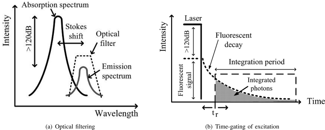
Fluorescence techniques find wide application in life sciences and are ideally suited for biomolecular detection both in vivo and in vitro. Targets molecules of interest, difficult to detect otherwise, are labeled with fluorophores. When optically excited, these fluorescent labels emit light at a longer wavelength than the excitation source. The difference in peak wavelengths between excitation and emission is referred to as the Stokes shift, typically 50nm–100nm. Precise optical filtering (of typically more than 160 dB) must be employed in almost all fluorescence applications for background rejection, filtering out the excitation light as shown in Fig. 1(a). Sensitive photodetection approaches, including cooled CCD imagers and photomultiplier tubes (PMTs), then measure the fluorescent signal.
Fig. 1.
Excitation/background rejection in fluorescence detection.
One of the most pervasive in vitro applications of fluorescence is in surface-based biomolecular (DNA, protein) assays [1]. In this case, fluorescently-labeled analyte targets from solution bind to complementary probe molecules immobilized on a passive solid support. Confocal laser scanners are then employed to image these arrays. In traditional microarrays, issues of sensitivity, accuracy, specificity, and reproducibility limit the reliability of the platform. Fluorescent techniques are also widely employed in vivo to observe the location of labelled molecules [2]. Imaging systems in this case include both wide-field epifluorescent microscopes and confocal laser-scanning microscopes.
Fluorophores have associated with them a characteristic lifetime, which defines the exponential fluorescent decay transient after the removal of the excitation source, as shown in Fig. 1(b). Fluorescent lifetimes are sensitive to excited-state reactions such as fluorescent resonant energy transfer (FRET) [4], enabling a growing field of fluorescent lifetime imaging microscopy (FLIM) [5]. The ability to time resolve fluorescent lifetimes on the same platform also enables detection of multiple fluorescent dyes simultaneously, similar to multi-color detection. Lifetimes, on the order of nanoseconds for organic dyes and longer for quantum dots [6], can be imaged spatially with detectors capable of fast time-gating. Such time-gated, time-resolved fluorescence detection also provides additional advantages in improved background rejection.
Time-resolved applications require a detector that is fast, as determined by the time-constant(s) of the impulse response, and sensitive, as determined by the minimum detectable integrated photon flux (photons/cm2). In most commercial time-resolved systems, time-correlated single photon counting (TCSPC) is employed with PMT detectors and laser scanning, with time resolution limited by jitter and sensitivity limited by dark count [7]. Frame rates are typically limited to fewer than 0.2 frames/s [8]. Alternate time-resolved fluorescence detectors rely on CCD imagers and gated intensifiers [9]. Frame rates of up to 100 frames/s have been achieved for a small imager (120-by-60) [10] if only two points of the decaying exponential are sampled, which is suitable for some monoexponential lifetime characterization.
Our previous effort [11] at a CMOS time-resolved imager was specifically directed toward active microarray applications. This imager had quantization-noise limited sensitivities of more than 108 photons/cm2 and an impulse-response time constant of more than 1.1 ns, limited by a long ”tail” in the photocurrent response of the diode. In this work, we consider the design of a time-resolved 64-by-64 CMOS imager specifically targeted for high-frame-rate FLIM applications [12], which improves on our earlier efforts in several significant ways. Differential photodiodes (PD) are implemented to improve photocurrent impulse response and noise immunity while preserving fast time gating. Thirteen-bit data conversion produces read-noise-limited sensitivities. Correlated double sampling (both digital and analog) reduces 1/f noise, and active reset is employed to reduce pixel reset noise. These combined techniques produce an imager with sensitivities approaching 8.8×10⁶ photons/cm2, a timing resolution of better than 150 ps, impulse-response time constants of better than 800 ps, and frame rates of better than 300 frames/s with two points per transient waveform.
In Section II, we review the design issues associated with implementing a time-resolved imager based on a CMOS photodiode sensor. Section III describes design details of our time-resolved CMOS imager. A quantitative analysis of read noise is presented in Section IV. Section V presents measured characterization of the sensor and Section VI concludes.
II. TIME-RESOLVED FLUORESCENCE DETECTION WITH CMOS ACTIVE PIXEL SENSORS
The issues in utilizing CMOS active pixel sensors (APS) for time-resolved fluorescence detection include impulse response, background rejection, sensitivity, and dynamic range.
A. Impulse response
A fast impulse response is a necessary attribute for any time-resolved detector. The measured time-resolved response of a fluorophore is the convolution of the fluorophore response with the detector impulse response,
| (1) |
where hdet(t) is the impulse response of the detector and ifluor(t) is the fluorophore’s response to an ideal impulse excitation source. If the detector impulse response is significantly slower than the fluorophore response, this deconvolution cannot be done accurately. A slow detector impulse response also increases the requirement on optical filtering in order to achieve equivalent background rejection as described below.
B. Background rejection
Traditionally, fluorescence detection [13] requires external, dye-specific filters to achieve high SBR in non-time-resolved applications. Time-gated operation of the pixel, however, provides immediate enhancement to the signal-to-background ratio (SBR) without additional hardware. By gating the excitation source in the time domain and collecting only the photons emitted by the fluorescent dyes after the laser has been turned off, as shown in Fig. 1(b), it is possible to achieve a high SBR without external filters. The SBR in such time-gated operation can be written as
| (2) |
where tr denotes the start of the integration period after the excitation has been turned off, and isignal(t) and ibackground(t) are the resulting transient photocurrents due to the fluorescent signal and excitation background, respectively. Assuming the employed fluorophore exhibits an exponential decay that can be characterized by a single time constant, τfluor, the fluorescent emission after the removal of the excitation can be generalized as
| (3) |
where Φ is the incident excitation light flux, and K1 is a fluorophore-specific coefficient which indicates the percentage of incident photons being absorbed and converted into fluorescent photons under the condition of constant incident photon flux. This coefficient is generally the product of the absorption cross section, quantum yield, and surface concentration of the fluorophores, as well as the photo collection efficiency and quantum efficiency of the photodetector. The characteristic lifetime can range from a few hundred picoseconds for organic fluorophores to several tens of nanosecond for quantum dots.
Assuming the detector impulse response exhibits a dominant time constant, τdet, that is much larger than the excitation turn-off time. The collected background signal can be written as
| (4) |
where coefficient K2 determines the percentage of the total charge, caused by the excitation, actually collected by the photodetector, discounting any reflection and both fluorescent and non-fluorescent absorption in the optical path.
The SBR can then be approximated by
| (5) |
τdet must be much smaller than τfluor in order to increase SBR. If a fluorophore with a short lifetime is used such that τdet approaches τfluor in magnitude, tr must be increased to delay the start of the integration period in order to increase SBR. Unfortunately, this causes the sensor to miss integrating the bulk of the total fluorescent signal, degrading the signal-to-noise ratio (SNR).
C. Sensitivity
Most fluorescence systems relying on high-gain detectors such as photo-multiplier tubes (PMTs). In contrast, CMOS photodiodes have no inherent gain and must rely on low-noise amplification through an active pixel sensor (APS) design. In conventional CMOS imagers, long integration times [14] can be employed to increase SNR. In a time-resolved imager, however, a fixed transient photocurrent is available during each measurement cycle and averaging with multiple measurements must be employed to reduce temporal noise. For one measurement, the SNR is given by
| (6) |
where is the input-referred reset noise sampled in each measurement, is the sum of input-referred noise from all circuits employed while reading the signal in the pixel, and is the input-referred photon shot noise. Averaging of N measurements increases the SNR by a factor of , and can in principle, be used to reduce the noise floor to quantization noise limits. In practice, frame-rate requirements generally require other approaches to noise reduction to limit the amount of averaging required.
D. Dynamic range
While sensitivity is the most important design metric for fluorescence imagers, dynamic range (DR) is a consideration. The upper bound of the system DR in conventional CMOS APS imager is often determined by pixel non-linearity before saturation. In a time-resolved measurement, the DR of the system can be extended by delaying the beginning of the integration window (increasing tr as shown in Fig. 1(b)) such that the signal decays sufficiently to ensure non-saturation of the pixel. If the measured response is dominated by a single time constant, it is possible to extrapolate the time-resolved data back to the same initial time across different measurements independent of tr extending the system DR.
III. SYSTEM DESCRIPTION
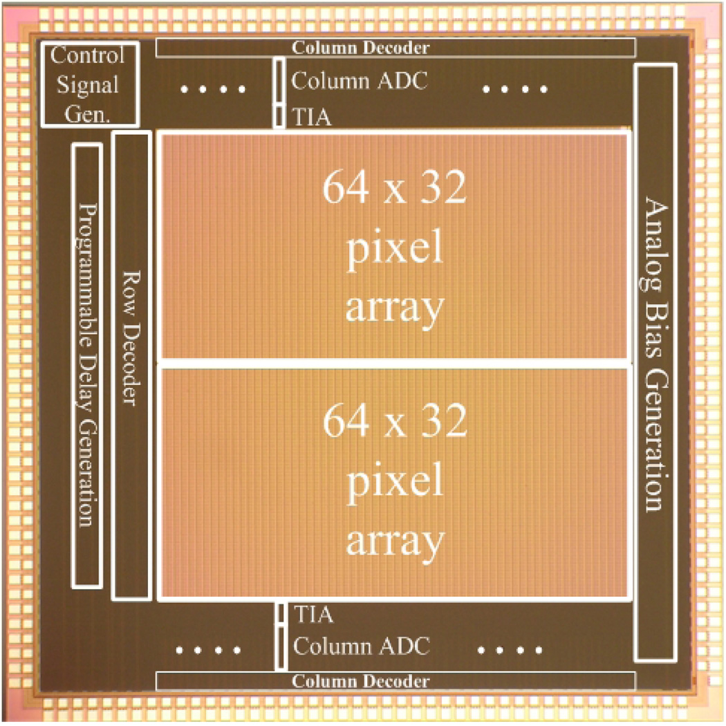
The chip micrograph of the 5-mm-by-5-mm array sensor as fabricated in a standard mixed-signal 0.18-µm process is shown in Fig. 2 [12]. The chip has 128 columns, each containing 32 active pixel sensors, one transimpedance amplifier (TIA), and one integrating analog-to-digital converter (ADC). These 128 columns are halved and end-abutted to form a square imager. Digital results from each ADC conversion are stored at the end of the conversion cycle, and each column decoder time-multiplexes and transmits stored data while the ADCs convert the next set of signals.
Fig. 2.
Chip micrograph of the array sensor.
A programmable delay generator controls the arrival time of the reset signal relative to the laser pulse. An on-chip digital controller generates appropriate signals for the TIAs and ADCs and synchronizes the excitation source and gated integration. To avoid noise from the digital circuitry, the pixel circuitry, TIA and most of the ADC have a separate dedicated set of supply voltages. Double guard rings are also placed around the analog circuits and pixel array to mitigate the effects of substrate noise. All analog signals are routed through one side of the chip while digital signals are separated and routed on the other three sides. We now consider the design of the pixel, TIA, and ADC in more detail. Overall design specifications are summarized in Table I.
TABLE I.
Chip Specifications and Measured Performance
| Item | Value |
|---|---|
| Technology | 0.18 µm |
| Die size | 5 mm × 5 mm |
| Pixel size | 50 µm × 50 µm |
| Array size | 64 × 64 |
| Active photodiode area | 576 µm2 |
| Quantum efficiency (at 650nm) | 0.42 |
| Delay line resolution | 150 ps |
| Signal path gain | 2 × 10⁻⁶ DN/(photons/cm2) |
| Sensitivity (with 64-point averaging) | 8.8 × 10⁶ photons/cm2 |
| Simulated pixel input-referred noise (with 64-point averaging) | 23.4 e− |
| Measured pixel input-referred noise (with 64-point averaging) | 21.3 e− |
| Simulated pixel impulse response time constant | 860 ps |
| Measured pixel impulse response time constant | 796 ps |
| ADC conversion time (single-ramp) | 102 µs |
| ADC conversion time (dual-ramp) | 1.6 µs |
| Frame rate (dual-ramp) | 310 frames/s |
| Power Consumption | 250 mW |
A. Differential Pixel
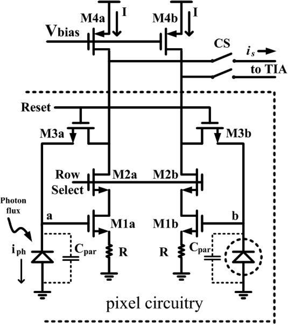
Each pixel contains a differential photodiode (PD) and a differential transconductance amplifier which amplifies and transmits the integrated signal current-mode to the column TIA as shown in Fig. 3. Photocurrent iph collected within the integration period Tint appears as a differential voltage between node a and node b in Fig. 3, where . Cpar is the total capacitance at node a and node b, and is approximately 198.7 fF for this pixel design. Active reset-noise suppression is performed by the transconductor (M1a, M1b) through the negative feedback switch (M3a, M3b).
Fig. 3.
Schematic of the differential pixel and column amplification.
Differential PD
In this design, the photodiodes are implemented with n-well/p-substrate junctions to maximize the quantum efficiency in the optical range. The impulse response of the diode is determined by by the convolution of the intrinsic photocurrent response and the RC time constant determined by the reset transistor and the diode capacitance, both of which must be made faster. Each pixel is 50-µm-by-50-µm with a total photodiode area of 576-µm2, leading to a fill factor of 23%.
For the pixel shown in Fig. 3, the equivalent RC time constant at the diode node during reset τD,reset, as determined by the equivalent triode-region conductance (gd,M3a) of the reset devices (M3a, M3b) and the total capacitance at the diode node, is given by
| (7) |
where CPD is the diode junction capacitance, CM1a,gate is the gate capacitance of transistor M1, and CM3a,drain is the drain capacitance of transistor M3. In this design the reset devices have and τD,reset is approximately 250 ps, making the diffusive component of the photocurrent impulse response the dominant factor in determining the overall pixel impulse response.
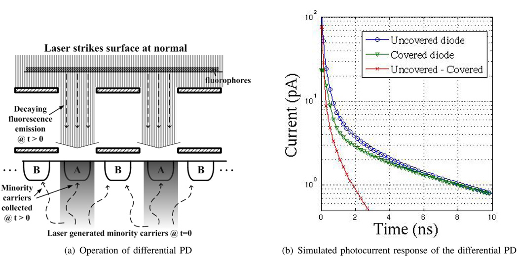
In conventional CMOS PDs, the photocurrent impulse response is determined by minority carriers generated within a diffusion length of the depletion region of the PD, which create a long ”tail” as they diffuse and are collected. To attenuate this diffusive component, a fingered differential PD is used, as shown in Fig. 4(a), in which alternating fingers are covered with metal [15], rendering the diffusive component of the photocurrent common-mode. The size of these fingered pixels is limited by n-well spacing rules, with the number of fingers determined by common-mode rejection requirements. In this design, each pixel contains a total of eight PD fingers; each finger is 3.2 µm wide and 45 µm long. Finger periodicity, defined as the sum of finger width and spacing, is 4.8 µm. For a given PD type and size, this common-mode rejection of the diffusive tail improves with increasing wavelength as the absorption depth increases. It can also be expected to improve with technology scaling as minimum n-well spacing decreases. Fig. 4(b) shows the simulated photocurrent response of the covered and uncovered diode. The resulting differential impulse response is also shown. The impulse response time constant of the differential diodes, or τdet in Eqn. 5, is expected to be approximately 860 ps from these simulations, compared with over 9 ns for a single-ended diode.
Fig. 4.
Differential PD.
Active reset
Reset noise is usually the most dominant component of temporal noise in a typical CMOS APS [16]. However, it is possible to reduce reset noise, , with an active reset [17] which in this design is implemented through a common-source amplifier (transistors M1a and M1b) that negatively feeds back to the PD during reset [18][19]. This pixel circuit is similar to a current-mode sample-and-hold (S/H) circuit [20], the noise performance advantages of which [21] are similar to CMOS APS active reset implementations [17][18][19]. In order to suppress reset noise effectively, the bandwidth of the transconductance amplifier, formed by transistor M1 and resistor R, must be larger than the the diode bandwidth, during reset. Since we seek and gm,M1 is the transconductance of transistor M1 during reset, this leads to the requirement that Gm,pixel >> gd,M3a=0.8 mS.
Differential transconductor
The pixel transconductors, which implement the active reset also perform differential voltage-to-current conversion with gain Gm,pixel for the pixel during integration. Nonsilicided polysilicon resistors are added to linearize the transconductor through source degeneration. The differential current signal from the transconductor is routed to the column-wise TIA. For intensity measurements, correlated double sampling (CDS), as described below, is used to mitigate the fixed pattern noise (FPN) that results from mismatch. In time-resolved measurements, such offsets do not affect performance since time series results are numerically differentiated.
B. Transimpedance Amplifier
The column TIA converts the differential current from the pixel into a voltage, with a resistance of for subsequent column-level data conversion, where Gm,OTA is the transconductance of the operational transconductance amplifier (OTA) shown in Fig. 5(a). Direct current-mode data conversion can also be configured, in which case the TIA is configured to operate as a current-mode sample-and-hold. The resistance RTIA can be adjusted to provide an overall conversion gain of
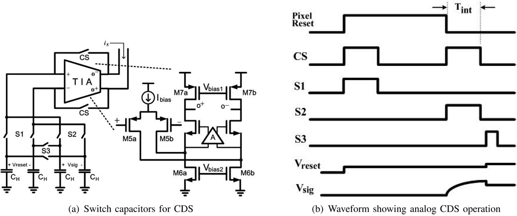
| (8) |
Large MOS capacitors CH of 1 pF are used to hold the value of the converted differential voltage as shown in Fig. 5. The settling time at the holding capacitor RTIACH, typically 1.2 ns, does not affect the detector impulse response as it is much shorter than typical integration times. Large capacitors CH keep the temporal noise in the column circuits significantly below that of the pixel reset. Correlated double sampling (CDS) is implemented in both analog and digital forms with the circuits shown in Fig. 5(a). To implement analog CDS, switched capacitors are used to store signals captured during reset (Vreset) and after photocurrent integration (Vsig) as shown in Fig. 5(b). The difference between these two signals is taken when switch S3 closes, after the second sampling period has completed, yielding a differential voltage equivalent to . CDS can also be performed digitally, in which both samples are converted to digital values right after each of the integration periods and the difference taken digitally. In digital CDS, S1 and S2 are always on and S3 is always off such that sampling capacitance is twice that of analog CDS, lowering sampled kTC noise. Digital CDS works best for this system, allowing 1/f to be reduced to the data converter quantization noise limit and exploiting the larger values for the sampling capacitors. Analog CDS could allow 1/f noise to be reduced below these quantization noise limits, but this has no practical import in this case because of the integrated data conversion.
Fig. 5.
Circuits and operations of CDS.
C. Analog-to-Digital Converter
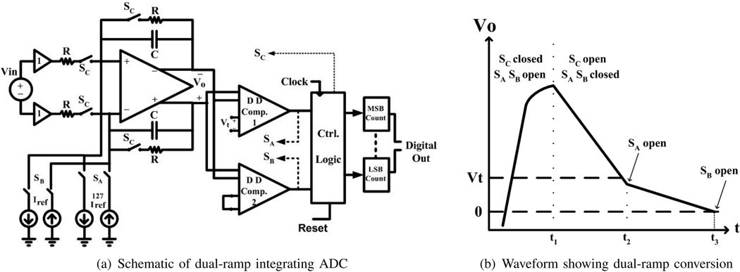
A per-column integrating ADC is employed due to its relatively small area, low power, and high resolution. The conversion time of a conventional single-ramp, single-slope integrating ADC is limited by both ADC resolution and comparator speed. In our design, we seek a 13-bit resolution. We have a comparator capable of detecting a minimum (LSB) input voltage difference of 24.4 µV in 12.5 ns. In a single-ramp architecture this results in a 102 µs conversion time, which is insufficient for FLIM applications at video rate, where multiple conversions must also be performed for a single pixel in order to achieve noise-reducing objectives. In order to achieve at least 300 frames-per-second frame rates while allowing for 32-row-multiplexing, 64-point-averaging, and lifetime resolution of at least two points per transient, a differential dual-ramp, single-slope ADC architecture [22] is implemented as shown in Fig. 6(a). This dual-ramp ADC architecture delivers a conversion time of 1.6 µs, 64-times faster than the single-ramp implementation using the same counter clock period, Tclock, requiring only an additional set of comparators and reference current sources. This exact speed up is given by one-half the ratio of coarse to fine reference currents, as described below.
Fig. 6.
Circuits and operations of ADC.
Dual-ramp operation starts each conversion by closing switches SC and opening switches SA and SB, sampling the input voltage at the output of the differential amplifier as shown in Fig. 6(b). At the start of the discharge/integration phase, the SC switches are open while both SA and SB are closed, discharging the output with coarse current, 128·Iref. The differential voltage VO decreases until it falls below the comparator threshold voltage Vt, at which time the top comparator in Fig. 6(a) signals the disconnection of switch SA at the start of the next clock period. To utilize the counters efficiently, Vt is set to the voltage level discharged by 128Iref in one clock period. Fine integration continues with fine reference current Iref until the differential voltage at the output of the amplifier drops below zero. The most-significant-bit (MSB) counter stores the number of clock cycles required for coarse integration, as defined by the number of clock cycles between t1 and t2 in Fig. 6(b), while the least-significant-bit (LSB) counter measures the number of cycles required for fine integration, defined by the time between t2 and t3. Accuracy in the dual ramp operation is degraded by any mismatch between coarse and fine reference current sources. The ADC can operate as a single-ramp converter for better accuracy (but lower conversion rate) by combining both counters as a single counter and leaving SA open during the entire integration phase. With a column conversion gain, Acolumn of eight and ADC fine reference current, Iref, of 0.74 nA, the overall gain of the entire sensor path is approximately 2 × 10⁻⁶ DN/(photons/cm2).
IV. NOISE ANALYSIS
Although averaging can reduce overall temporal noise, a frame rate requirement of at least 300 frames/s in real-time FLIM applications limits the amount of averaging per frame to 64. Efforts must to be made to reduce temporal noise to reduce averaging requirements. The dominant noise components include pixel reset noise, pixel transconductor noise, TIA sample-and-hold noise, and the quantization noise of the ADC. Read noise sources are calculated below and summarized in Table II.
TABLE II.
Summary of Calculated Read Noise Without Averaging
| Item | Input-referred noise (rms) |
|---|---|
| Reset noise | 186.4 e− |
| Pixel readout noise | 12.9 e− |
| Quantization noise | 0.4 e− |
| Total | 187.9 e− |
Pixel Reset Noise
With the use of active reset, the reset noise on Cpar in Fig. 3 is reduced by a factor equal to where go,M3a is 0.8 mS. The mean-squared noise voltage at the differential inputs of the pixel transconductor due to reset is, therefore,
| (9) |
The reset noise at this node can also be expressed as the average noise charge
| (10) |
leading to an rms input-referred noise charge of 186.4 e− (see Table II).
Pixel Transconductor and TIA Noise
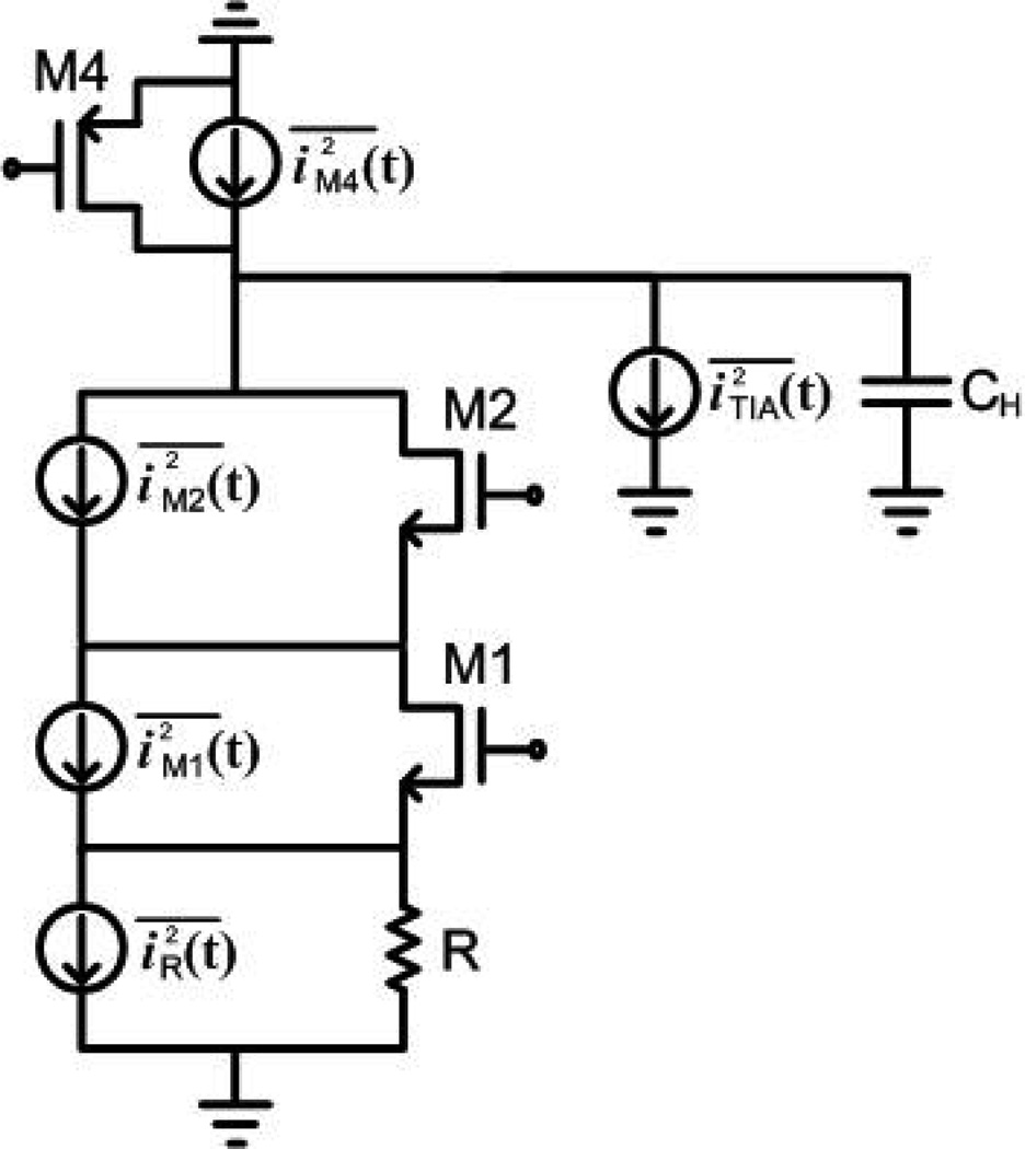
The pixel transconductor noise is dominated by the thermal noise of transistors M1a and M2a and the biasing device M4a shown in Fig. 3. The equivalent half-circuit model for noise analysis during signal amplification is shown in Fig. 7, in which iR(t), iM1(t), iM2(t), iM4(t) are thermal noise sources associated with each device in the pixel transconductor and iTIA(t) represent the sum of all thermal noise sources in the OTA of Fig. 5(a) where is defined as for comparison with noise sources from the pixel. noise effects are rendered insignificant due to CDS and are excluded in this calculation. Assuming steady state operation, it can be shown that the constituent output-referred mean-squared differential noise voltages due to pixel readout are given by
| (11) |
| (12) |
| (13) |
| (14) |
| (15) |
where gm,M1 and go,M1 are the transconductance and output conductance of M1, gd,M2 is the channel conductance of M2, and gm,M4 is the transconductance of transistor M4 in Fig. 3. is given by
| (16) |
which includes the noise contributions of the transistors in the OTA as shown in Fig. 5(a) during readout. Since only one set of CH capacitor is shared among the pixels in a column, they can be made much larger than Cpar, suppressing the effect of pixel transconductor noise on overall read noise. If digital CDS is employed, CH becomes 2CH in these expressions as the two holding capacitors are configured in parallel and the total input-referred mean-squared noise voltage from the pixel transconductor during readout is calculated to be
| (17) |
Fig. 7.
Small-signal model for noise analysis during readout.
The total input-referred mean-squared noise charge is then
| (18) |
leading to an rms input-referred noise charge of 12.9 e− (see Table II).
Quantization Noise
Since we expect to employ averaging to reduce total temporal noise, the ADC must be able to set the LSB to be much lower than the calculated temporal noise in order to gain the benefits of averaging. The input-referred quantization step size at the pixel can be calculated as . Assuming quantization error is not correlated, the input-referred mean-squared quantization noise voltage and charge are calculated as
| (19) |
| (20) |
leading to an rms input-referred noise charge of 0.4 e− (see Table II) and allowing more than 240000 samples to be taken for averaging to reduce the dominant temporal noises before this quantization noise limit is reached.
V. RESULTS
In this section, we present measured characteristics of the array sensor (summarized in Table I) as well as results using the array for time-resolved fluorescence detection.
A. Array characteristics
Quantum efficiency
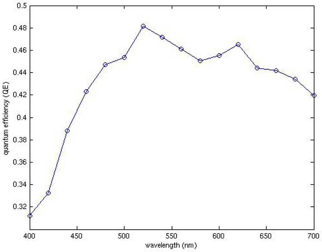
Fig. 8 shows the measured external quantum efficiency (QE) using a standard measurement setup including a monochromator, integrating sphere, and calibrated photodiode. Measured QE peaks just slightly above 40% for incident wavelengths between 600 nm and 650 nm.
Fig. 8.
Quantum efficiency of fingered n-well/p-sub photodiode sensor.
Time domain characterization
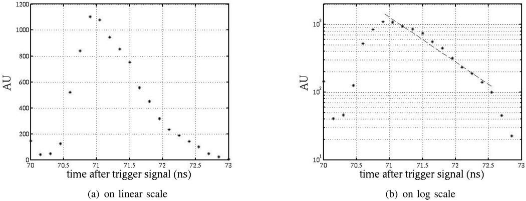
Fig. 9 is the measured impulse response of the pixel. A PiLas Picosecond Laser Diode System with a 406-nm laser diode head is used for this measurement. This gain-switched laser is capable of producing laser pulses of less than 50-ps FWHM with peak collimated beam power as high as 150 mW. The laser pulses are synchronized with the chip. Results come from 4096-point averaging and numerically differentiating the resulting imager response. The data show that the system has an impulse response with a time constant of less than 800 ps. With fingered PD periodicity of 4.8 µm, this result agrees with both our simulated results shown in Fig. 4(b) and that found in [15] for similar finger periodicity.
Fig. 9.
Differentiated time-resolved detection of laser turn-off edge.
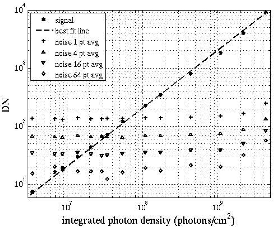
Sensitivity characterization
Fig. 10 shows measured sensor sensitivity, taken by integrating the entire laser pulse by positioning the reset turnoff before the laser pulse. Neutral density filters are added to vary the intensity of the laser signal. The noise floors are shown for different amounts of averaging. Simulation predicts a reset-noise-limited sensitivity of approximately 188 e− without any averaging, which corresponds to a photon density of 7.3 × 10⁷ photons/cm2, assuming 45% quantum efficiency. Measured noise floors determine a sensitivity of approximately 7.0 × 10⁷ photons/cm2 (SNR of 0 dB) without averaging, which is within 10% of the simulated results. Measurements also show 64-point averaging improves this sensitivity by a factor of eight, as expected, to 21.3 e− or 8.8 × 10⁶ photons/cm2.
Fig. 10.
Measured sensor system sensitivity.
B. Applications
Preliminary results are presented using the array in two applications, as an active substrate for microarray applications and as a FLIM imager in epi-fluorescent microscopy. In the former case, fluorescent labels are directly immobilized on the chip surface. Time-gating is relied upon to achieve the required SBR. In the later case, the imager acts as a camera and relies on the optics of the microscope for image acquisition. Filter cubes are employed for additional background rejection.
Microarray measurements
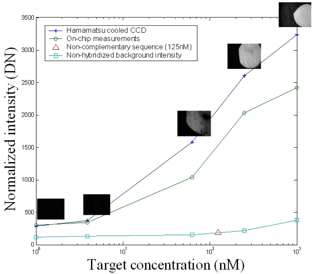
The chips are packed in ball-grid packages which are ”doughnut” epoxy encapsulated, providing access to the sensor area while protecting the bond wires. The chip surface is cleaned and epoxy-derivatized with 3-glycidoxypropyltrimethoxysilane. Aminated DNA probes with a length of 21 nucleotides are immobilized on top of the detector area through contact-pin spotting. DNA hybridizations are carried out with analyte solutions containing different concentrations of matching DNA (target 1) strands, which are end-labeled with biotin molecules. Hybridizations with non-complemetary (target 2) sequences are also carried out as a control. Probe and target sequences are given in Table III. After hybridization, streptavidin-conjugated Qdot-655 (Invitrogen) solution is used to label and quantify the amount of hybridization and thus the concentration of matching target DNA molecules in the original analyte solution. Data from on-chip detection is verified by also imaging the chip surface in an epi-fluorescence microscope with a Hamamatsu cooled CCD imager and 500nm long-pass filter cube. The results from different target concentrations in the hybridization analyte solutions are shown in Fig. 11, and show correlation between chip and CCD measurements. Hybridization sensitivity is primarily limited by non-specific binding of either target DNA molecules or fluorescent labels to the substrate surface, rather than the sensitivity of the sensor.
TABLE III.
Oligonucleotide Sequences Used in Active Microarray Experiments
| Label | Sequence |
|---|---|
| Probe | 5’-CTGAACGGTAGCATCTTGAC-3’ |
| Target1 | 5’-GTCAAGATGCTACCGTTCAG-3’ |
| Target2 | 5’-CAATACTTCGGTGGCATGAC-3’ |
Fig. 11.
Measured DNA hybridization for various target concentrations.
Lifetime imaging application
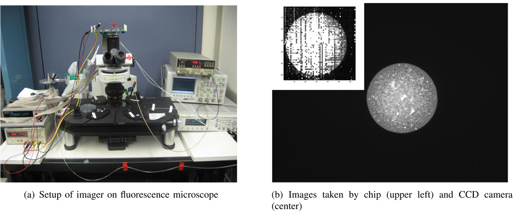
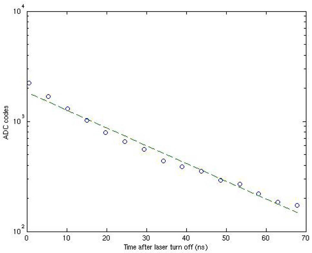
This chip can also function as a fluorecence lifetime imager when it is attached to the standard c-mount camera port of an Olympus BX51W1 fluorescence microscope as shown in Fig. 12a. Using an integration period of 16 ms, a fluorescence image of an immobilized spot of Qdot-655, conjugated with streptavidin on top of epoxy-derivitized glass, is taken with the chip and shown in the insert of Fig 12b. The same fluorescent spot is also taken with a Hamamatsu ORCA-ER cooled CCD camera using the same exposure time, and shown in the same figure for comparison. A 10X objective lens is used and the diameter of the fluorescent spot is estimated to be 300 µm. The surface coverage of Qdot-655 is estimated to be 3.2 × 1013 cm−2. Fig. 13 shows a measured lifetime response at a single pixel. This measurement shows this particular fluorophore exhibits a lifetime of 19.6 ns.
Fig. 12.
Images of a fluorescent spot taken on a microscope.
Fig. 13.
Measured fluorescence lifetime of Qdot-655.
VI. CONCLUSION
In this paper, we have described the implementation of a CMOS imager specifically designed for fluorescence lifetime imaging through a time-gated differential pixel design. These pixels possess an impulse response of less than 800 ps through an optically differential photodiode. The array has a measured sensitivity of 21.3 e-/pixel with 64-pt averaging. Future work involves demonstrating the imager in a high frame rate FLIM application as well as demonstrating an active microarray application of gene expression profiling with clinical samples. Demonstration of the device, as an active substrate in fluorescence-based surface bioassay detecting genetic material from physiological samples, will be reported in a biotechnology journal.
ACKNOWLEDGMENT
The authors would like to thank UMC for chip fabrication.
The project described was supported in part by Award Number R33HG003089 from the National Human Genome Research Institute. This work was also supported in part by the NSF under grant BES-428544, by NYSTAR, and by the C2S2 Focus Center Research Program.
Biographies

Ta-chien D. Huang Ta-chien D. Huang received the B.S. degree in electrical engineering from Columbia University, New York, NY, in 1997 and the M.S. degree in electrical engineering from Stanford University, Stanford, CA, in 1999. From 1999 to 2003, he was a member of technical staff with Sun Microsystems Inc., Velio Communications Inc. and Netlogic Microsystems Inc., designing high speed I/O and mixed-signal integrated circuits. Since 2003, he has been pursuing the Ph.D. degree in electrical engineering at Columbia University. His research interests include integrated circuit design for biosensing applications, computational systems biology, and high performance analog/mixed-signal integrated circuit design.
Mr. Huang received the Myril B. Reed Best Paper Award of the 49th MWSCAS in 2007.

Sebastian Sorgenfrei Sebastian Sorgenfrei received the B.A. degree in physics from Williams College, Williamstown, MA in 2005 and the B.S. and M.S. degree in electrical engineering from Columbia University, New York, NY in 2005 and 2006. Since 2006, he has been pursuing the Ph.D. degree in electrical engineering at Columbia University.
His research interests include analog/mixed-signal integrated circuit design, carbon nanotube devices and novel interfaces for biosensor applications. He has held internship positions at Porsche AG, Infineon Technologies AG and Robert Bosch LLC.

Ping Gong Ping Gong received the B.S. degree in chemistry from Peking University,Beijing, China in 1999 and the Ph.D. degree from Colorado State University, Fort Collins, CO in 2006 in analytical chemistry. She has since worked as a postdoctoral research associate at Columbia University in the Departments of Chemical and Electrical Engineering. Her research interests include the development of electrochemical methods in the characterization and quantification of surface DNA hybridization behavior for biosensing applications and the development of bio-conjugation, microarray surface fabrication,characterization, and fluorescence quantum dot detection methods for integratedCMOS biosensor applications.
Dr. Gong is a member of the American Chemical Society and the American Vacuum Society.

Rastislav Levicky Rastislav Levicky holds a PhD degree in chemical engineering from the University of Minnesota, Minneapolis (1996), and a BS in chemical engineering from Columbia University, New York, NY (1991). His PhD thesis focused on self-organized polymer assemblies at solid-liquid interfaces and in thin films. From 1996 to 1998 he was a National Research Council Postdoctoral Associate with the National Institute of Standards and Technology (NIST) in Gaithersburg, MD, where he studied the interfacial organization and biological activity of polynucleic acids with neutron beam and optical techniques. In July 1998 he joined the Chemical Engineering faculty at Columbia University, from where he moved to the Department of Chemical and Biological Engineering at Polytechnic Institute of New York University in July 2006. His current research interests encompass biointerfacial engineering, biomolecular diagnostics, kinetics of interfacial reaction networks, and electrochemistry. Dr. Levicky is a member of the American Institute of Chemical Engineers, the American Chemical Society, the American Physical Society, and the American Vacuum Society. He is a recipient of the National Science Foundation CAREER Award for Young Investigators, and the 2001 Distinguished Faculty Teaching Award from Columbia University Engineering Alumni Association.

Kenneth Shepard Kenneth L. Shepard (M’91-SM’03-F’08) received the B.S.E. degree from Princeton University, Princeton, NJ, in 1987 and the M.S. and Ph.D. degrees in electrical engineering from Stanford University, Stanford, CA, in 1988 and 1992, respectively. From 1992 to 1997, he was a Research Staff Member and Manager with the VLSI Design Department, IBM T. J. Watson Research Center, Yorktown Heights, NY, where he was responsible for the design methodology for IBM’s G4 S/390 microprocessors. Since 1997, he has been with Columbia University, New York, where he is now Professor. He also was Chief Technology Officer of CadMOS Design Technology, San Jose, CA, until its acquisition by Cadence Design Systems in 2001. His current research interests include design tools for advanced CMOS technology, on-chip test and measurement circuitry, low-power design techniques for digital signal processing, low-power intrachip communications, and CMOS mixed-signal design for biological applications.
Dr. Shepard was Technical Program Chair and General Chair for the 2002 and 2003 International Conference on Computer Design, respectively. He has served on the Program Committees for ISSCC, VLSI Symposium, ICCAD, DAC, ISCAS, ISQED, GLS-VLSI, TAU, and ICCD. He received the Fannie and John Hertz Foundation Doctoral Thesis Prize in 1992, a National Science Foundation CAREER Award in 1998, and the 1999 Distinguished Faculty Teaching Award from the Columbia Engineering School Alumni Association. He has been an Associate Editor of IEEE TRANSACTIONS ON VERY LARGE-SCALE INTEGRATION (VLSI) SYSTEMS and is current an Associate Editor for the IEEE JOURNAL OF SOLID-STATE CIRCUITS.
Contributor Information
Ta-chien D. Huang, Email: tachien@cisl.columbia.edu, Columbia Bioelectronics Systems Laboratory, Department of Electrical Engineering, Columbia University, New York, NY 10027 USA.
Sebastian Sorgenfrei, Email: sorgenfrei@cisl.columbia.edu, Columbia Bioelectronics Systems Laboratory, Department of Electrical Engineering, Columbia University, New York, NY 10027 USA.
Ping Gong, Email: gongping@cisl.columbia.edu, Columbia Bioelectronics Systems Laboratory, Department of Electrical Engineering, Columbia University, New York, NY 10027 USA.
Rastislav Levicky, Email: rlevicky@poly.edu, Department of Chemical and Biological Engineering. Polytechnic University, Brooklyn, NY 11201 USA.
Kenneth L. Shepard, Email: shepard@cisl.columbia.edu, Columbia Bioelectronics Systems Laboratory, Department of Electrical Engineering, Columbia University, New York, NY 10027 USA.
REFERENCES
- 1.Schena M, et al. Microarrays: Biotechnology’s discovery platform for functional genomics. Trends Biotechnology. 1998 Jul.vol. 16:301–316. doi: 10.1016/s0167-7799(98)01219-0. [DOI] [PubMed] [Google Scholar]
- 2.Sekar R, Periasamy A. Fluorescence resonance energy transfer (FRET) microscopy imaging of live cell protein localizations. J. Cell. Biology. 2003 Mar.vol. 160(no. 5):629–633. doi: 10.1083/jcb.200210140. [DOI] [PMC free article] [PubMed] [Google Scholar]
- 3.Draghici S, Khatri P, Ehlund AC, Szallasi Z. Reliability and reproducibility issues in DNA microarray measurements. Trends in Genetics. 2006 Feb.vol. 22(no. 2):101–109. doi: 10.1016/j.tig.2005.12.005. [DOI] [PMC free article] [PubMed] [Google Scholar]
- 4.Chen Y, Mills J, Periasamy A. Protein localization in living cells and tissues using FRET and FLIM. Differentiation. 2003 Dec.vol. 71(Iss. 9–10):528–541. doi: 10.1111/j.1432-0436.2003.07109007.x. [DOI] [PubMed] [Google Scholar]
- 5.Bastiaens PIH, Squire A. Fluorescence lifetime imaging microscopy: Spatial resolution of biochemical processes in the cell. Trends Cell Biology. 1999 Feb.vol. 9:58–52. doi: 10.1016/s0962-8924(98)01410-x. [DOI] [PubMed] [Google Scholar]
- 6.Michalet X, et al. Quantum Dots for living cells, in vivo imaging, and diagnostics. Science. 2005 Jan.vol. 307:538–544. doi: 10.1126/science.1104274. [DOI] [PMC free article] [PubMed] [Google Scholar]
- 7.Yotter RA, Wilson DM. A review of photodetectors for sensing light-emitting reporters in biological systems. IEEE Sensors J. 2003 Jun.vol. 3(no. 3):288–303. [Google Scholar]
- 8.Becker W, et al. Fluorescence lifetime imaging by time-correlated single-photon counting. Microscopy Research and Techniques. 2004;vol. 63:58–66. doi: 10.1002/jemt.10421. [DOI] [PubMed] [Google Scholar]
- 9.Mitchell AC, Wall JE, Murray JG, Morgan CG. Direct modulation of the effective sensitivity of a CCD detector: a new approach to time-resolved fluorescence imaging. J. Microscopy. 2002 Jan.vol. 206(pt. 3):225–232. doi: 10.1046/j.1365-2818.2002.01029.x. [DOI] [PubMed] [Google Scholar]
- 10.Agronskaia AV, Tertoolen L, Gerritsen HC. Fast fluorescence lifetime imaging of calcium in living cells. Journal of Biomedical Optics. 2004 Nov.vol. 9:1230–1237. doi: 10.1117/1.1806472. [DOI] [PubMed] [Google Scholar]
- 11.Patounakis G, Shepard KL, Levicky R. Active CMOS array sensor for time-resolved fluorescence detection. IEEE JSSC. 2006 Nov.vol. 41(no. 11):2521–2530. [Google Scholar]
- 12.Huang T, Sorgenfrei S, Shepard KL, Gong P, Levicky R. A CMOS array sensor for sub-800-ps time-resolved fluorescence detection. IEEE CICC. 2007 Sep.:829–832. doi: 10.1109/JSSC.2009.2016994. [DOI] [PMC free article] [PubMed] [Google Scholar]
- 13.Sander D, et al. Low-noise CMOS fluorescence sensor. IEEE ISCAS. 2007 May [Google Scholar]
- 14.Eltoukhy H, Salama K, El Gamal A. A 0.18 µm CMOS bioluminescence detection lab-on-chip. IEEE JSSC. 2006 Mar.vol. 41(no. 3):651–662. [Google Scholar]
- 15.Genoe J, et al. Calculation of the current response of the spatially modulated light CMOS detector. IEEE Trans. Electron Devices. 2004 Nov.vol. 48(no. 9):1891–1902. [Google Scholar]
- 16.Tian H, Fowler B, El Gamal A. Analysis of temporal noise in CMOS photodiode active pixel sensor. IEEE JSSC. 2001 Jan.vol. 36(no. 1):92–101. [Google Scholar]
- 17.Fowler B, Godfrey MD, Balicki J, Canfield J. Low noise readout using active reset for CMOS APS. Proc. SPIE. 2000 May;vol. 3965:126–135. [Google Scholar]
- 18.Kozlowski LJ, et al. Pixel noise suppression via SoC management of tapered reset in a 1920×1080 CMOS image sensor. IEEE JSSC. 2005 Dec.vol. 40(no. 12):2766–2776. [Google Scholar]
- 19.Yang J, et al. A 3Mpixel low-noise flexible architecture CMOS image sensor. ISSCC Dig. Tech. Papers. 2006 Feb.:496–497. [Google Scholar]
- 20.Daubert SJ, Vallancourt D, Tsividis YP. Current copier cells. Electron. Lett. 1988 Oct.vol. 24:1560–1562. [Google Scholar]
- 21.Daubert SJ, Vallancourt D. A transistor-only current-mode ΣΔ modulator. IEEE JSSC. 1992 May;vol. 27(no. 5):821–830. [Google Scholar]
- 22.van de Plassche R. Analog-To-Digital and Digital-To-Analog Converters. New York: Springer; 1994. [Google Scholar]


