Microelectronic systems utilizing organic materials afford many advantages over traditional silicon-based systems. Organic electronic devices have potential manufacturing advantages including solution processing and large scale fabrication with reduced cost. Organic devices can also be easily fabricated on polymeric substrates, which are suitable for a broad range of flexible electronics applications including conformal devices and displays, and would also be potentially suitable for roll-to-roll fabrication strategies. For example, many types of organic devices including transistors, sensors, and photovoltaic cells have been fabricated on both natural and synthetic flexible polymers including poly(ethylene terepthalate),[1-3] poly(imide),[4] poly(ether sulfone),[5] cellulose,[6, 7] and silk fibroin.[8] Various organic polymeric systems composed of biodegradable polymers[9] have demonstrated utility in many applications including temporary medical implants[10, 11] and compostable products.[12] For example, thermoplastic polyesters such as poly(L-lactide-co-glycolide) (PLGA) are commonly used biodegradable polymer for drug delivery systems and medical implants while poly(4-hydroxybutyrate) (P4HB) is commonly used as a biodegradable plastic for disposable products.[13] Water soluble polymers such as dextran and poly(vinyl alcohol) have been used for a variety of biomedical applications including tissue engineering scaffolds[14] and environmental applications.[15] Recent progress in the design and synthesis of organic semiconductors have led to the realization of molecules that can operate stably in hydrated or oxidative environments[16] including p-channel materials based on thiophenes[17] or fluorenes,[18] and n-channel materials based on perylene diimides.[19] These concomitant advancements in organic electronics and biodegradable polymers processing suggest that there is the potential for the use of biodegradable polymeric systems for the development of biodegradable electronic devices for potential use in biomedical or environmental applications. Toward this end, we investigated materials and fabrication strategies for the realization of organic thin film transistor using a small molecule semiconductor in combination with a biodegradable polymeric substrate and dielectric. We demonstrate that these devices perform stably after exposure to water and since they consist of nearly entirely biodegradable materials, these devices are resorbable in an in vitro degradation environment.
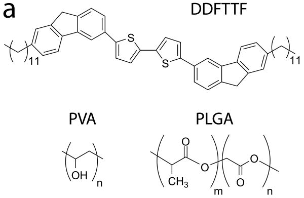
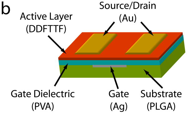
A schematic of the device is shown in Figure 1. The strategy for material selection focused on utilizing materials that are biocompatible and biodegradable yet would also exhibit adequate electronic properties and suitable device processing capability. The biomaterials selected for the substrate and dielectric layer should exhibit a unique intersection of biological and electronic properties that would also be compatible with a variety of polymer processing techniques. From a biomaterial perspective, the materials should be resorbable, exhibit excellent biocompatibility profiles, and ideally would have been previously utilized in biomedical devices that have been approved by the United States Food and Drug Administration (FDA). These polymers should be soluble in orthogonal solvent systems to promote facile processing methods including casting and spin coating. These constraints on material properties led to the selection of PLGA and PVA polymers to be used as the substrate and gate dielectric, respectively, in this device. PLGA and PVA polymers are inexpensive, commercially available, and have been previously used in a wide array of biomedical devices for clinical applications.
Figure 1.
Materials Selection and Device Configuration of Organic Thin Film Transistors. (a) The chemical structures of the semiconductor (DDFTTF), the dielectric (PVA), and the substrate (PLGA) are shown. (b) These materials are processed into devices in top-contact configuration as shown. Briefly, PLGA was melt-processed into substrates approximately 1 × 1 cm2 in area and 2 mm in thickness. Silver gate contacts were evaporated through a shadow mask. PVA dielectrics were spin coated from solution followed by thermal evaporation of DDFTTF semiconducting layers and gold source-drain contacts. The final device geometry contained channel lengths of 50 μm and a W/L ratio of 20.
The semiconducting molecule utilized in this study consists primarily of a large core consisting of conjugated substituents. 5,5′-bis-(7-dodecyl-9H-f luoren-2-yl)-2,2′-bithiophene (DDFTTF) is a robust small molecule p-channel semiconductor that exhibits excellent device performance is resistant to harsh environments including aqueous conditions.[17] Although the biodegradation of DDFTTF has not been explicitly studied, degradation mechanisms that are used to decompose melanin,[20, 21] a conjugated amorphous semiconductor,[22, 23] could potentially be expanded in a similar manner to DDFTTF. Therefore, we elected to deposit DDFTTF as the active layer through thermal evaporation. The choice of conducting metals for electrical contacts was based primarily on process considerations, yet both are potentially suitable for use in medical devices. Silver exhibits suitable biocompatible in vitro and in vivo and has been used as an antimicrobial agent in biomedical implants for a variety of clinical applications.[24, 25] Gold is an inert biomaterial that has exhibited reduced biofouling in vivo for various biomedical implants including cardiovascular[26] and BioMEMS devices.[27]
The substrate, which composes 99.89% of the total mass of the device, was chosen to consist of PLGA, a linear biodegradable thermoplastic polyester. PLGA with a high relative amount of lactic acid was chosen (PLGA 85:15) because of the elevated Tg, which allows for processing at elevated temperatures. The surfaces of melt processed PLGA substrates were extremely smooth with Rms roughness of 0.46 nm, which facilitated subsequent device fabrication. However, the physical properties of thermoplastic PLGA provided limitations in downstream device processing due to: (1) low melting point (Tm) and glass transition temperatures (Tg), and (2) solubility in common organic solvents. These properties suggest the use of mild downstream processing conditions and the use of water-soluble PVA as a solution processable dielectric, respectively. PVA is water-soluble environmentally biodegradable polymer[15] that has also demonstrated reasonable utility in organic electronics.[28] PVA exhibits a large dielectric constant and is processable into thin films with a small free volume: these properties would ultimately serve to reduce operating voltages and gate leakage currents. PVA also has the ability to be photocrosslinked by incorporating ammonium dichromate (ADC) and irradiating films with UV, which enables the possibility of photolithographically defined features. High molecular weight electrical grade PVA (Mw ∼ 205,000 Da) was processed into relatively thick PVA films (1.3 μm) for two primary reasons: (1) to reduce the gate leakage current and (2) to mask this roughness and prevent electrical short defects between the gate and source-drain electrodes. Although they exhibit relatively lower capacitance values, PVA dielectrics on the order of 1 μm have been shown to serve as effective dielectric layers (Table 1).[29, 30] Non-crosslinked PVA (nPVA) and photo-crosslinked PVA (xPVA) films exhibited Rms roughness of 0.31 and 0.24 nm, respectively.
Table 1.
Summary of Device Performance for DDFTTF-based transistors on PVA dielectrics with PLGA substrates. Devices fabricated on non-crosslinked poly(vinyl alcohol) (nPVA) exhibited higher mobilities, higher on-off ratios, and smaller threshold voltages compared to devices fabricated on photocrosslinked poly(vinyl alcohol) (xPVA). Frequency distributions are shown in Figure S3.
| Dielectric Material | Dielectric Constant, k | Capacitance, Cd [nF-cm-2] | Mobility, μ [cm2-sec-1-V-1] | Threshold Voltage, VT [V] | On-off Ratio, Ion/Ioff |
|---|---|---|---|---|---|
| nPVA | 7.6 | 5.20 | 0.207 ± 0.069 | -15.4 ± 1.7 | 5.5 ± 2.1 × 10³ |
| xPVA | 6.7 | 4.56 | 0.057 ± 0.018 | -18.9 ± 4.9 | 3.2 ± 0.69 × 10³ |
DDFTTF films evaporated at 50 °C on both nPVA and xPVA exhibited island morphologies with extremely high aspect ratio features (Figure S1). Enhanced performance is observed in DDFTTF if the substrate is maintained at approximately 95 °C during deposition.[17] However, the maximum substrate temperature that could be achieved using PLGA substrates was nominally 50 °C. This lower temperature could lead to relatively reduced transistor performance as compared to previous studies.[17] This resulted in rough films with Rms roughness values of 21.14 and 19.45 nm, respectively. Conductive gate electrodes fabricated through rapid thermal deposition of silver enabled the formation of films nominally 15-20 nm in thickness without macroscopic defects. Rapid deposition simultaneously produced silver films with relatively large roughness with an Rms roughness of 4.32 nm. Silver was used as the gate electrode because of the ability to achieve high deposition rates, which resulted in relatively smooth films on the PLGA substrate. Gold films of similar thickness deposited at a rate of 1 Å-sec-1 for 200 sec exhibited micron scale roughness and precluded subsequent dielectric processing. However, gold was suitable for use in the source-drain contacts.
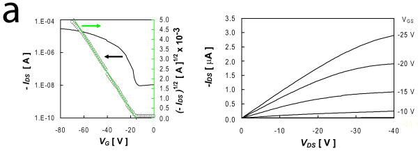
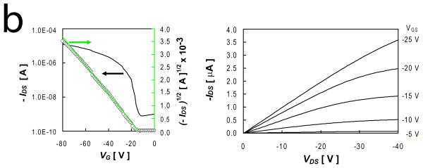
Thin film transistors based on p-channel DDFTTF active layers and PVA dielectrics exhibited electron mobilities as high as 0.253 cm2-sec-1-V-1 and on-off current ratios (Ion/Ioff) up to 9.4 × 10³ (Table 1, IFigure 2). Devices fabricated on nPVA films exhibited generally enhanced performance compared to similar devices fabricated on xPVA dielectrics (Fig. S3). This includes enhanced mobility, increased Ion/Ioff, and reduced VT (Table 1, *** p < 0.001 for all metrics). The origin of the effect on crosslinking PVA dielectric films on resulting mobility is likely to be through the alteration of the dielectric constant. The dielectric constants of nPVA and xPVA films, 7.6 and 6.7 respectively, were observed to be comparable with other solution-processed PVA films.[29-31] This reduction is likely due to the conversion of free hydroxyl groups into ether groups upon free radical polymerization. Furthermore, this reduction is comparable to previous reports.[30, 31] Other reports have demonstrated that only slight alterations in dielectric constant can result in up to three-fold alterations in mobility,[32] a similar span that was roughly observed in this work. The pendant hydroxyl groups at the interface could serve as the primary reason for the reduced observed mobilities. Additionally, the hydroxyl groups at the PVA interface could also limit the ability to achieve saturation in the output characteristics of the device (Figure 2), an effect that was observed in other devices that employ PVA as a dielectric material.[30] PVA dielectrics exhibited leakage currents on the order of 10-5 A-cm2 and < 10-5 A-cm2 at VGS = -20 V for nPVA and xPVA films, respectively. These higher leakage currents could serve to reduce the maximum drain current and ultimately result in lower Ion/Ioff than previous reports that employed DDFTTF semiconducting channels.[17]
Figure 2.
Electrical Performance of Representative DDFTTF-Based Transistors Fabricated on PLGA Substrates. Transistors fabricated from thermally evaporated DDFTTF semiconducting layers exhibited relatively high mobilities and on-off ratios on both (a) nPVA and (b) xPVA dielectrics. The device performance metrics for the device depicted in (a) are μ = 0.153 cm2-sec--1-V-1, Ion/Ioff = 3.49 × 10³, and VT = -15.6 V. The device performance metrics for the device depicted in (b) are μ = 0.060 cm2-sec--1-V-1, Ion/Ioff = 2.93 × 10³, and VT = -13.6 V.
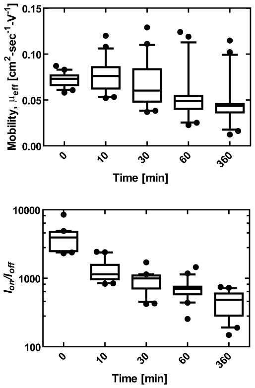
Future potential applications of these devices in biomedical or environmental applications presupposes the possibility of stable device operation after exposure to aqueous conditions. Transistors fabricated on xPVA dielectrics exhibited adequate performance after direct exposure of the semiconducting layer to liquid water for extended periods of time (Figure 3). Exposure of the device to water led to reduced effective mobility (μeff), reduced Ion/Ioff, and a shift in VT from approximately 18.9 ± 4.9 V to 2.82 ± 7.3 V. Exposure of the DDFTTF semiconductor material led to a dramatic increase in the off current, which is likely due to high concentrations of hydroxide and hydronium ions entering the semiconductor-dielectric interface. Similar trends were observed for exposure of DDFTTF on poly(4-vinyl-phenol) dielectrics as well.[17] It should be noted that exposure of device to water using nPVA dielectrics resulted in immediate device failure due to delamination of the structure. Devices fabricated on both nPVA and xPVA substrates also immediately failed after exposure to phosphate buffered saline, which can likely be attributed to the high concentration of inorganic ionic species (∼ 160 mM). The sensitivity of device performance to ionic species suggests that appropriate encapsulation and packaging of the device must be achieved before the possibility of utilizing this device in aqueous environments with high ion concentrations.
Figure 3.
Effect of Aqueous Exposure to Device Performance. The kinetics of electrical performance as a function of cumulative time exposed to ddH2O is shown for a set of 20 devices. Effective mobility (μ,eff) was measured to decrease gradually over the course of 6 hr. Ion/Ioff was immediately reduced upon exposure to liquid water and then very gradually decreased over the remainder of the time course.
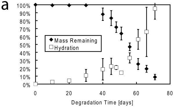
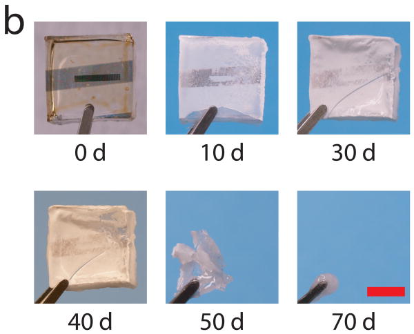
In vitro biodegradation studies were performed to investigate device resorption characteristics. Our primary goal was not to make a device that would operate in the presence of a harsh environment. Rather, we wanted to show that these devices can indeed degrade under biological conditions. Exposing devices to citrate buffer led to the irreversible loss of device functionality in less than 2 days as the DDFTTF layer of the device delaminated from the dielectric. The mass loss kinetics of the device, which is composed primarily of the PLGA substrate, was characterized thereafter (Figure 4a). The mass loss progression of devices fabricated on PLGA 85:15 substrates observed in this study was similar to that of previous studies of PLGA mass loss through hydrolysis mechanisms.[33-35] The devices were relatively resistant to mass loss and water uptake for approximately 30 days. After this time, there was a significant decrease in mass and corresponding increase in hydration as the device began undergoing rapid autocatalytic hydrolysis and bulk erosion. The observed degradation time scale was consistent with previous reports as well for this particular PLGA formulation.[33, 36] The mass loss kinetics exhibited a significant lag time, during which water infiltration into the device, followed by rapid degradation. Significant mass loss and water uptake was observed thereafter. Structural integrity was lost at approximately 50 days of degradation time at which point the device was primarily composed of a viscous gel composed of low molecular weight PLGA (Figure 4b).
Figure 4.
In Vitro Degradation of Devices. a) A plot of mass remaining and water uptake by mass (hydration) demonstrates that devices fabricated on PLGA substrates were initially resistant to mass degradation and water uptake. However, after 30 days, significant mass loss and water uptake was initiated. Near total mass loss and 100% device hydration was observed at 70 days. b) Photographs from representative devices at various stages of the degradation time line suggest that device integrity was intact up until 40 days with near total device resorption at 70 days. Devices also transitioned from being initially optically transparent (0 days) to opaque within 10 day. Scale bar represents 5 mm for all panels.
Herein we describe the design, fabrication, and characterization of water-stable organic thin film transistors fabricated using biodegradable and biocompatible polymers. These devices maintained functionality after direct exposure to water and are principally resorbable as demonstrated through in vitro degradation studies. The potential utilization of resorbable organic electronics could serve as a motivating factor for the development of high performance dielectrics and semiconducting molecules with the additional properties of biocompatibility and biodegradability into non-toxic and environmentally safe monomers. These degradation products than could then be incorporated into metabolic pathways in order to undergo subsequent degradation steps. For example, recent work has examined the possibility of using DNA-based dielectrics for organic electronic applications.[37] The future development of advanced encapsulation materials and techniques based on resorbable materials would help to expand the set of operating environments for this class of devices to include in vivo environments. One could design different encapsulation schemes to expand the operating conditions and control the rate of degradation of electronic as well as physical properties. Tailoring the packaging of these structures could also lead to pre-programmed device lifetimes by virtue of temporally mediating exposure of critical device components to caustic environments. The device functionality presented in this work is the first step towards realizing more complex biodegradable and compostable electronic devices. Subsequent design, fabrication, and integration of other simple electronic components fabricated from resorbable electronically active materials could be utilized in the realization of temporary medical implants with electronic functionality. For example, resorbable implants with electronic capability could be utilized as next generation electroactive drug delivery systems[38, 39] or tissue engineering scaffolds.[40] Biodegradability could also be advantageous in utilizing compostable electronic devices in environmentally sensitive settings.
Experimental
Device Fabrication
All materials were used as received unless otherwise noted. Poly(L-lactide-co-glycolide) (85:15, Mw = 50,000-70,000 Da, Sigma-Aldrich, St. Louis, MO USA) was melted and cast into substrates with dimensions of approximately 1 cm × 1 cm × 2 mm (W × L × t) using fluoropolymer-coated silicon substrates heated to approximately 200 °C using a hot plate. A conductive gate electrode was deposited by thermal evaporation of silver (Ag) through a shadow mask at 15-20 Å-sec-1 for 10 sec to create a conductive film 15-20 nm in thickness. Poly(vinyl alcohol) (PVA, Moliol 40-88, Sigma-Aldrich) solutions at a concentration of 10% (w/v) in double distilled water (ddH2O) were spin coated to form the gate dielectric layer. Ammonium dichromate (ADC, Sigma-Aldrich) was used as a photocrosslinking agent by dissolving into PVA solutions at a mass ratio of 1:6 ADC:PVA. Solutions were filtered using a 0.45 μm poly(vinylidene fluoride) filter (Millipore, Billerica, MA USA) prior to spin coating. PVA solutions were spin coated on to substrates at 3000 RPM for 40 sec. PVA films with ADC were photocrosslinked at λ = 254 nm for 10 min followed by rinsing with ddH2O to remove residual ADC. All films underwent a dehydration bake at 50 °C for 18 h under 27 in Hg vacuum. 5,5′-bis-(7-dodecyl-9H-f luoren-2-yl)-2,2′-bithiophene (DDFTTF) was chosen as the semiconductor for its stability in aqueous environments. DDFTTF was synthesized and purified as previously reported [17]. DDFTTF films were deposited by thermal evaporation (Angstrom Engineering, Kitchener, Ontario, Canada) at a rate of 0.2– 0.4 Å-sec-1 under a pressure of 5.0 × 10⁻⁷ Torr. The temperature of the substrates was kept at 50 °C during deposition. Gold source-drain electrodes were thermally deposition through a shadow mask to form device channels 50 μm in length with a W/L ratio of 20.
Physical Device Characterization
PVA dielectric films were fabricated into metal-insulator-metal capacitors with gold as the top and bottom contacts. Film morphology was characterized by atomic force microscopy (AFM) (NanoScope IV, Digital Instruments, Plainview, NY USA) operated in tapping mode (300-kHz frequency, Si tip). Film thicknesses were determined by profilometry (Dektak 150 Profilometer, Veeco, Plainview, NY USA)
Electronic Device Characterization
The electrical measurements were carried out in ambient by using a Keithley 4200SCS semiconductor parameter analyzer equipped with KITE Interactive and a standard probe station setup. Values for mobility (μ) and threshold voltage (VT) were calculated by operating devices in the saturation regime and applying Equation 1:
| (1) |
Dielectric capacitance (Cd) measurements were performed by using a Hewlett–Packard 4192 LF Impedance Analyzer for frequencies ranging between 20 Hz and 100 KHz. Samples Unpaired Student's t-tests were performed where appropriate with significance values set at * p < 0.05, ** p < 0.01, and *** p < 0.001 (GraphPad Prism, La Jolla, CA USA). All values are reported as mean ± s.d. unless otherwise stated. Box-whisker plots indicate lower and upper quartiles with 10-90 percent confidence interval, respectively. Outliers beyond this range are shown as discrete points. At least 60 devices were characterized for dry performance characteristics and at least 20 devices were characterized at each time point for water exposure experiments.
Degradation Studies
Devices with xPVA dielectrics were dedicated for biodegradation studies (n = 4) and were incubated in citrate buffer (pH = 4.0) at 37 °C. Macroscopic photos were taken with an Olympus E520 camera. Devices were removed at predetermined time points, washed with ddH2O, pat dried, and weighed to obtain mwet(t). Samples were then dried under vacuum for 4 days at 35 °C to remove all moisture and the devices were measured again to obtain mdry(t). Mass loss and device hydration were determined from Equations 2 and 3 as follows:
| (2) |
| (3) |
where m(t) is the mass at a given time t and m(to) is the initial mass.
Supplementary Material
Acknowledgments
The authors would like to acknowledge the assistance of Debbie Lin and Anatoly Sokolov for assistance in sample preparation and instrumentation. Financial support for this project was provided by the National Institutes of Health (Grant #1F32NS064771-01) and the Office of Naval Research (N000140810654) MURI project. CJB was funded by a Ruth L. Kirschstein NIH fellowship.
References
- 1.Roberts ME, Mannsfeld SCB, Stoltenberg RM, Bao Z. Org Electron. 2009;10:377. [Google Scholar]
- 2.Briseno AL, Tseng RJ, Ling MM, Falcao EHL, Yang Y, Wudl F, Bao Z. Adv Mater. 2006;18:2320. [Google Scholar]
- 3.Rogers JA, Bao Z, Baldwin K, Dodabalapur A, Crone B, Raju VR, Kuck V, Katz H, Amundson K, Ewing J, Drzaic P. Proc Nat Acad Sci USA. 2001;90:4835. doi: 10.1073/pnas.091588098. [DOI] [PMC free article] [PubMed] [Google Scholar]
- 4.Someya T, Kato Y, Sekitani T, Iba S, Noguchi Y, Murase Y, Kawaguchi H, Sakurai T. Proc Nat Acad Sci USA. 2005;102:12321. doi: 10.1073/pnas.0502392102. [DOI] [PMC free article] [PubMed] [Google Scholar]
- 5.Kushto GP, Kim W, Kafafi ZH. App Phys Lett. 2005;86:093502. [Google Scholar]
- 6.Fortunato E, Correia N, Barquinha P, Pereira L, Goncalves G, Martins R. IEEE Elect Dev Lett. 2008;29:988. [Google Scholar]
- 7.Yong-Hoon K, Dae-Gyu M, Jeong-In H. IEEE Elec Dev Lett. 2004;25:702. [Google Scholar]
- 8.Kim DH, Kim YS, Kaplan JADL, Omenetto FG, Zakin M, Rogers JA. 2009 doi: 10.1063/1.3238552. [DOI] [PMC free article] [PubMed] [Google Scholar]
- 9.Gross RA, Kalra B. Science. 2002;297:803. doi: 10.1126/science.297.5582.803. [DOI] [PubMed] [Google Scholar]
- 10.Tamai H, Igaki K, Kyo E, Kosuga K, Kawashima A, Matsui S, Komori H, Tsuji T, Motohara S, Uehata H. Circulation 2000. 102:399. doi: 10.1161/01.cir.102.4.399. [DOI] [PubMed] [Google Scholar]
- 11.Middleton JC, Tipton AJ. Biomaterials. 2000;21:2335. doi: 10.1016/s0142-9612(00)00101-0. [DOI] [PubMed] [Google Scholar]
- 12.Paetau I, Chen CZ, Jane J. J Polym Environ. 1994;2:211. [Google Scholar]
- 13.Martin DP, Williams SF. Biochem Eng J. 2003;16:97. [Google Scholar]
- 14.Ferreira LS, Gerecht S, Fuller J, Shieh HF, Vunjak-Novakovic G, Langer R. Biomaterials. 2007;28:2706. doi: 10.1016/j.biomaterials.2007.01.021. [DOI] [PMC free article] [PubMed] [Google Scholar]
- 15.Chiellini E, Corti A, D'Antone S, Solaro R. Prog Polym Sci. 2003;28:963. [Google Scholar]
- 16.Mallik AB, Locklin J, Mannsfeld SCB, Reese C, Roberts ME, Senatore ML, Zi H, Bao Z. In: Organic Field Effect Transistors. Bao Z, Locklin J, editors. CRC Press; Boca Raton, FL USA: 2007. [Google Scholar]
- 17.Roberts ME, Mannsfeld SCB, Queraltó N, Reese C, Locklin J, Bao WKZ. Proc Nat Acad Sci USA. 2008;105:12134. doi: 10.1073/pnas.0802105105. [DOI] [PMC free article] [PubMed] [Google Scholar]
- 18.Locklin J, Ling MM, Sung A, Roberts ME, Bao Z. Adv Mater. 2006;18:2989. [Google Scholar]
- 19.Oh JH, Liu S, Bao Z, Schmidt R, Wurthner F. App Phys Lett. 2007;91:212107. [Google Scholar]
- 20.McGinness J, Corry P, Proctor P. Science. 1974;183:853. doi: 10.1126/science.183.4127.853. [DOI] [PubMed] [Google Scholar]
- 21.Napolitano A, Pezzella A, Vincensi MR, Prota G. Tetrahedron. 1995;51:5913. [Google Scholar]
- 22.Ito S. Pig Cell Res. 2003;16:230. doi: 10.1034/j.1600-0749.2003.00037.x. [DOI] [PubMed] [Google Scholar]
- 23.Bettinger CJ, Bruggeman JP, Misra A, Borenstein JT, Langer R. Biomaterials. 2009;30:3050. doi: 10.1016/j.biomaterials.2009.02.018. [DOI] [PMC free article] [PubMed] [Google Scholar]
- 24.Bosetti M, Massè A, Tobin E, Cannas M. Biomaterials. 2002;23:887. doi: 10.1016/s0142-9612(01)00198-3. [DOI] [PubMed] [Google Scholar]
- 25.Massè A, Bruno A, Bosetti M, Biasibetti A, Cannas M, Gallinaro P. J Biomed Mater Res B. 2000;53:600. doi: 10.1002/1097-4636(200009)53:5<600::aid-jbm21>3.0.co;2-d. [DOI] [PubMed] [Google Scholar]
- 26.Edelman ER, Seifert P, Groothuis A, Morss A, Bornstein D, Rogers C. Circulation. 2001;103:429. doi: 10.1161/01.cir.103.3.429. [DOI] [PubMed] [Google Scholar]
- 27.Voskerician G, Shive MS, Shawgo RS, Recum Hv, Anderson JM, Cima MJ, Langer R. Biomaterials. 2003;24:1959. doi: 10.1016/s0142-9612(02)00565-3. [DOI] [PubMed] [Google Scholar]
- 28.Kim SH, Yang SY, Shin K, Jeon H, Lee JW, Hong KP, Park CE. App Phys Lett. 2006:89. [Google Scholar]
- 29.Maliakal A. In: Organic Field Effect Transistors. Bao Z, Locklin J, editors. CRC Press; Boca Raton, FL USA: 2007. [Google Scholar]
- 30.Jin SH, Yu JS, Lee CA, Kim JW, Park BG, Lee JD. J Kor Phy Soc. 2004;44:181. [Google Scholar]
- 31.Singh TB, Meghdadi F, Gunes S, Marjanovic N, Horowitz G, P PL, Bauer S, Sariciftci NS. Adv Mater. 2005;17:2315. [Google Scholar]
- 32.Jang Y, Kim DH, Park YD, Cho JH, Hwang M, Choa K. App Phys Lett. 2005;87:152105. [Google Scholar]
- 33.Lu L, Garcia CA, Mikos AG. J Biomed Mater Res. 1999;46:236. doi: 10.1002/(sici)1097-4636(199908)46:2<236::aid-jbm13>3.0.co;2-f. [DOI] [PubMed] [Google Scholar]
- 34.Bettinger CJ, Bruggeman JP, Borenstein JT, Langer RS. Biomaterials. 2008;29:2315. doi: 10.1016/j.biomaterials.2008.01.029. [DOI] [PMC free article] [PubMed] [Google Scholar]
- 35.Wang Y, Kim YM, Langer R. J Biomed Mater Res A. 2003;66:192. doi: 10.1002/jbm.a.10534. [DOI] [PubMed] [Google Scholar]
- 36.Lu L, Peter SJ, Lyman MD, Lai HL, Leite SM, Tamada JA, Uyama S, Vacanti JP, Robert L, Mikos AG. Biomaterials. 2000;21:1837. doi: 10.1016/s0142-9612(00)00047-8. [DOI] [PubMed] [Google Scholar]
- 37.Stadler P, Oppelt K, Singh TB, Grote JG, Schwödiauer R, Bauer S, Piglmayer-Brezina H, Bäuerle D, Sariciftci NS. Organic Electronics. 2007;8:648. [Google Scholar]
- 38.Prescott JH, Lipka S, Baldwin S, Sheppard NF, Maloney JM, Coppeta J, Yomtov B, Staples MA, Santini JT. Nat Biotechnol. 2006;24:437. doi: 10.1038/nbt1199. [DOI] [PubMed] [Google Scholar]
- 39.Santini JT, Cima MJ, Langer R. Nature. 1999;397:335. doi: 10.1038/16898. [DOI] [PubMed] [Google Scholar]
- 40.Radisic M, Park H, Shing H, Consi T, Schoen FJ, Langer R, Freed LE, Vunjak-Novakovic G. Proc Nat Acad Sci USA. 2004;101:18129. doi: 10.1073/pnas.0407817101. [DOI] [PMC free article] [PubMed] [Google Scholar]
Associated Data
This section collects any data citations, data availability statements, or supplementary materials included in this article.


