Abstract
The release of neurotransmitters and hormones from secretory vesicles plays a fundamental role in the function of the nervous system including neuronal communication. High-throughput testing of drugs modulating transmitter release is becoming an increasingly important area in the fields of cell biology, neurobiology, and neurology. Carbon-fiber amperometry, provides high-resolution measurements of amount and time course of transmitter release from single vesicles, and their modulation by drugs and molecular manipulations. However, such methods do not allow the rapid collection of data from a large number of cells. To allow such testing, we have developed a CMOS potentiostat circuit that can be scaled to a large array. In this paper, we present two post-CMOS fabrication methods to incorporate the electrochemical electrode material. We demonstrate by proof of principle the feasibility of on-chip electrochemical measurements of dopamine, and catecholamine release from adrenal chromaffin cells. The measurement noise is consistent with the typical electrode noise in recordings with external amplifiers. The electronic noise of the potentiostat in recordings with 400 μs integration time is ~0.11 pA and is negligible compared to the inherent electrode noise.
Keywords: biosensors, transmitter release, amplifier array, post-processing, chromaffin cell, amperometry, quantal release
I. Introduction
In response to specific signals, many eukaryotic cells release pre-formed molecules packaged into secretory vesicles that fuse with the plasma membrane and release their contents into the extracellular space. This process is called exocytosis. The released contents of a single vesicle represent a unit or quantum and quantal size refers to the number of molecules released from a single vesicle. Various transmitter molecules, such as dopamine or its conversion products adrenaline and noradrenaline, are readily oxidizable, and hence quantal release events can be measured as brief current spikes using carbon-fiber-electrode (CFE) amperometry [1] with high resolution. The drug L-Dopa, which provides symptomatic relief to patients with Parkinson’s disease, increases the quantal size, while amphetamines decrease the quantal size [2]–[4]. The high-resolution amperometric current traces exhibit foot signals, that have a typical amplitude of 1–10 pA [5], and which indicate the slow flux of catecholamines through a narrow fusion pore [6]. Quantification and analysis of the foot-signal properties can lead to valuable knowledge of the fusion pore structure and dynamics. However, CFE amperometric experiments are slow and laborious requiring a large number of single-cell experiments to obtain statistically significant data on the effects of various drugs [7]. Miniaturized high-performance CMOS biosensor arrays have the potential to provide high-throughput recording of amperometric events and subsequently provide statistically significant data. In recent years, several CMOS devices have been developed for applications to such diverse fields of study as drug design, neurobiology, DNA sequence analysis and cellular metabolism [8]–[11]. CMOS potentiostats for the electrochemical detection of biomolecules, for measuring ion channel current, and for cyclic voltammetry using off-chip transducers have been developed [12]–[17]. Recently, wireless circuits for in vitro measurement of dopamine using amperometry [18], as well as in vivo detection of dopamine using fast-scanning cyclic voltammetry [19], [20] were developed. CMOS chip designs have also been developed for electrochemical on-chip recordings [21], [22]. However, for practical use a suitable polarizable working electrode material needs to be incorporated such as gold or platinum. On-chip gold electrodes have been incorporated into a four by four active sensor array for cyclic voltammetry [23], which requires measurement of large currents and which is not suitable for the resolution of sub-pA currents associated with the detection of quantal transmitter release events. We recently described a CMOS potentiostat design that is scalable to an array, that would allow simultaneous high-resolution on-chip measurement of exocytosis from a large number of cells, that meets the requirements of high time resolution, and that has an electronic noise of ~0.11 pA for a 400 μs integration period [22].
In this paper, we describe the post-CMOS deposition of polarizable electrode material on the on-chip aluminum electrodes and packaging of the chip to enable on-chip experiments. Using a single potentiostat circuit, we demonstrate the ability of the potentiostat circuit to measure electrochemical reactions and cellular exocytotic events with high sensitivity. In Section II, we describe the post-CMOS fabrication techniques employed to incorporate the transducer onto the potentiostat circuit. In Section III, we describe the experimental setup, materials, and methods used to conduct on-chip electrochemical measurements. In Section IV, we discuss the experimental results. Finally in Section V, we summarize the paper and describe our vision of developing a large-scale array for measuring electrochemical currents.
II. Post-CMOS Fabrication
Several biomolecules and neurotransmitters are oxidizable, and therefore can be measured as an amperometric current trace. In order to oxidize these molecules, an appropriate transducer electrode is required. Typical transducer electrode materials include carbon, platinum, and gold. The CMOS chip was fabricated using AMIS C5F 0.5 μm technology. The interconnect material used in this technology is Al, but Al is not a suitable material for electrochemistry. The transducer electrode that facilitates electrochemical reactions is called a polarizable electrode [25]. When a polarizable electrode is immersed in salt solution, no current flows through the electrode-liquid interface. When a voltage is applied to the polarizable electrode, excess charge accumulates on the electrode surface, and is counter balanced by the ionic charge in the electrolyte solution at a finite distance from the metal electrode called the Debye length [26]. Current does not flow through the interface when the voltage is held constant. However, when oxidizable molecules diffuse to the surface of the electrode, electrons are transferred, and a Faradaic current is generated. Therefore, the surface of the Al electrode must be covered with a polarizable electrode material. Here, we describe polarizable material deposition using two methods: focused-electron-beam deposition of platinum and physical vapor deposition of gold/platinum using photolithography.
A. Focused-Electron-Beam Deposition
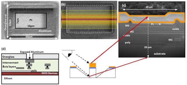
During the development phase of new CMOS circuit techniques, small-geometry dies are preferred because they are economical. However, post-CMOS fabrication of small-geometry dies present several challenges including handling the chips. On small geometry CMOS dies, platinum can be deposited with relative ease using the focused-ion-beam (FIB) or focused-electron-beam techniques. The FIB system is generally used by circuit designers to make device/circuit edits on prototype integrated circuits, in order to correct simple mistakes in and to test minor alterations to circuits without going through a whole fabrication cycle. This system facilitates making metal connections, disconnections and probe pads. The metal that can be deposited using the FEI strata 400 Dual Beam FIB system at the Cornell Center for Materials Research (CCMR) is platinum. Using a low-current (<100 pA) focused ion beam, the native oxide layer on Al is milled away. Precursor gases flowing over the chip interact with the electron column. The electron-beam-induced chemical reaction results in the deposition of Pt with sub-micron-scale resolution on the electrode surface, as shown in Fig. 1a. For electrochemical on-chip recordings, the electrode was fully covered with Pt (Fig. 1b). The composition of the deposited amorphous layer was platinum : carbon : gallium : oxide in proportions of 45 : 24 : 28 : 3, with a resistivity in the range of 70–700 μΩcm [27].
Fig. 1.
Post processed CMOS chips. (a) Top-view of Pt deposited on an Al pad using the focused electron beam. Openings in the over glass/passivation oxide layers are made at the CMOS foundry. Post CMOS processing includes the removal of the native oxide layer and deposition of the Pt layer. Only a portion of the Al pad is covered with platinum to show more clearly the contours of the deposited layer. (b, top) Al pad completely covered with a layer of 200 nm Pt as used for electrochemical on-chip detection. To inspect the chip for damage from the post-processing procedure, the central part (red box) was first covered with an additional layer of ~1 μm Pt for protection. Subsequently the areas indicated by the yellow boxes were milled away using the ion beam. (b, bottom) The resulting shape of the surface shows a central part that is exposed at its side to a depth of 10 μm and can be inspected when viewed from the side as indicated. (c) Cross-sectional view of the CMOS die after FIB processing as indicated in (b). No evidence for impurities is observed. The orange outline indicates the extra layer of platinum that was deposited to protect the sample during the processes of milling the sample. M1–M3 indicate the interconnect metal layers, oxide the SiO2 layers, and Pt is the platinized electrode surface. Poly indicates polysilicon used as conducting gate material and substrate the silicon wafer. Panel (c) was stretched vertically to show the layer structure. (d) Schematic of the CMOS die prior to post-CMOS fabrication. Openings in the overglass layer are made at the CMOS foundry.
The CMOS die is covered with a thick overglass layer, and this insulating layer gets charged under electron bombardment, which makes identification of regions of interest difficult. In order to alleviate these problems, the layout design must include alignment marks on the top metal layer, metal3, with openings in the overglass layer. In our case, the Al pads were not covered with the overglass layer, and thus were easily located. Penetration of impurities in the focused-electron-beam deposited film depends on the interaction between the electron beam and the sample, the beam current, and the grounding of the sample. The exposed Al pads could be located with a low-current electron beam without excessive charging, by properly grounding the chip. When a 5.0 kV, 25 pA electron beam was used to deposit the platinum layer, no evidence of damage was observed and the functionality of the CMOS chip was not affected. A schematic of the various layers of the circuit pre-FIB fabrication is shown in Fig. 1d, and a cross-sectional FIB image of the CMOS potentiostat circuit post fabrication is shown in Fig. 1c.
B. Photolithography
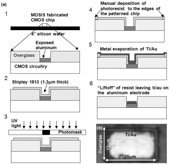
Focused-electron-beam deposition has the advantage of high resolution and ease of handling, but for larger areas and arrays with many electrodes, this method is too slow and involves chip exposure to the ion beam for extended periods to locate the electrodes, and may eventually alter the functioning of the circuit. As an alternative procedure, we investigated how physical vapor deposition of Ti/Au could be utilized for post-CMOS fabrication of the chip. A process flow diagram of the post-CMOS fabrication is shown in Fig. 2a. To allow proper handling, the small 2.5 mm × 2.5 mm CMOS die was attached to a 4″ photoresist-coated wafer and baked. Subsequently, a 1.3 μm thick photoresist (Shipley 1813) layer was spun on the chip surface. The photoresist is patterned using a tone-reversed photomask, exposing all areas except the Al electrodes. The chip was then developed (MF 321 for 60 sec) following image reversal. Photoresist spins off of the edges of the small CMOS die due to its rectangular shape, thus, the edges of the chip are initially not covered with photoresist. In some cases, the photoresist on the edges is stripped during the photomask contact. This was corrected by manual application of additional photoresist to the edges of the CMOS die (Fig. 2, step 4) before it was baked. The chip was then descummed (stripped of organic materials and residual photoresist) using GLEN 1000p plasma cleaning system in the electron-free mode. Electron-free mode prevents electrostatic damage. In the electron-free mode, the samples to be cleaned are placed on a floating shelf beneath the RF powered and ground shelf. Plasma is generated between the RF powered and ground shelf. Heavy plasma gas ions pass through the perforated ground shelf onto the samples, balancing the lighter electrons on the ground shelf and preventing surface charge buildup on the sample. The metal (Pt or Au) was vapor deposited over the entire surface. The next step was to lift-off photoresist along with the metal leaving behind only the metal in direct contact with the Al pads. The deposited metal forms the new electrode surface.
Fig. 2.
(a) Schematic of the process flow for deposition of polarizable material on Al electrodes using photolithography. There are six steps associated with the post-CMOS fabrication using photolithography. In the first step, the CMOS die is placed on a 4″ carrier wafer coated with photoresist and baked. The following steps illustrated in the figure do not show the carrier wafer. (b) Microscopic image of a single Al electrode coated with 10 nm Ti layer for adhesion and 200 nm Au layer.
C. Packaging
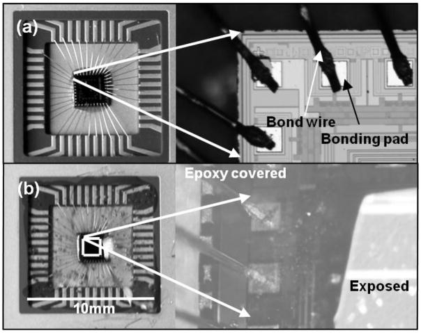
The CMOS die was epoxy glued to a dual-inline package (DIP), as shown in Fig. 3a. The package cavity along with the die was subsequently covered with epoxy (Devcon 5 minutes) to protect the sensitive bonding pads, wire bonds and connecting wires from contact with the electrolyte solution. Only the central part of the chip (inside the square in Fig. 3b) is left open, exposing only the surface of the CMOS die with electrodes (Fig. 3b). The layout of the chip is designed such that the electrodes are positioned in the center of the chip, spatially well separated from the I/O pads to avoid the epoxy encapsulating the active electrode area.
Fig. 3.
(a) A photograph of a CMOS chip in the package and a microscopic image of the bonding pads and wire bonds. (b) Photograph of the CMOS chip covered with epoxy excluding the boxed area. Microscopic image showing the epoxy covered and exposed areas
III. Materials and Methods
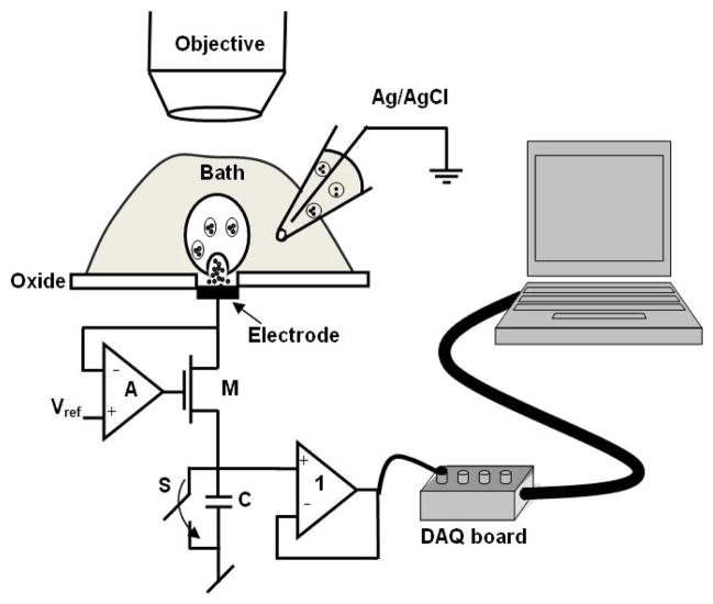
A schematic of the experimental setup is shown in Fig. 4. This schematic represents a single element of the proposed sensor array. In contrast to a conventional carbon-fiber apparatus, this device includes sensor circuits at the site of detection for improved sensitivity. A high-gain amplifier A holds the electrode at the oxidation potential of the target molecule and the transistor M conveys the electrons to the capacitor C, which is periodically reset by switch S. At the end of the integration period, the voltage on the capacitor is buffered to the data acquisition board (National Instruments PCI-6251). The recorded data is subsequently analyzed using the software program IGOR PRO (Wave Metrics, Lake Oswego, OR). The printed circuit board, along with the CMOS chip is mounted on an adjustable microscope (Ziess Axioskop 2) stage. The whole setup is housed in a properly grounded Faraday cage placed on a vibration isolation table.
Fig. 4.
Schematic of the experimental setup: The printed circuit board is mounted on an adjustable microscope stage. A pipette holder is placed on another adjustable microscope stage to position the pipette near the electrode. The microscope along with the adjustable holders is housed in a properly grounded faraday cage to eliminate power line noise. The output is connected to a 16-bit A/D converter, clocked externally to sample data at the end of the integration period. The A/D converter is connected to a computer where the data is acquired and analyzed.
A. Cell and Bath Solution Preparation
Bovine adrenal glands obtained from a local slaughterhouse were prepared according to established protocols [24]. The resulting chromaffin cells were suspended in the tissue culture medium and stored in a T-25 flask in a 10% CO2 incubator at 37 °C. Cells were used on days 1–3 in culture. On the day of the experiment, cells in the medium were transferred to a 15 mL tube and pelleted in a centrifuge at 5000 rpm for 10 minutes, and resuspended in 1–2 mL of bath solution. The bath solution contains 150 mM NaCl, 5 mM CaCl2, 5 mM KCl, 2 mM MgCl2, 10 mM HEPES buffer and 20 mM glucose. The osmolarity of the solution was measured to be 300–310 mOsm and the pH was 7.25.
IV. Experimental Results
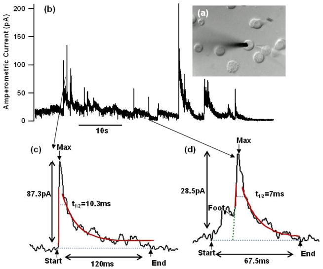
The first measurements of catecholamine release from chromaffin cells were performed with a 5 μm diameter CFE externally connected to the CMOS chip. The CFE extending from a pipette filled with 3 M KCl was positioned near a chromaffin cell (Fig. 5a). A Ag|AgCl wire placed in the same pipette translates ionic current to electronic current. The Ag|AgCl wire was connected to the input of the potentiostat circuit, which held the CFE at a potential of 0.7 V relative to a Ag|AgCl reference electrode placed in the solution bathing the cells. A second pipette filled with a bath solution containing 20 μM calcium ionophore ionomycin was positioned nearby. The cell was stimulated by ejecting ionomycin and the amperometric current that was recorded is shown in Fig. 5b. The amperometric current indicates the time course of the catecholamine release from the cell. Chromaffin cells release preferentially norepinephrine and epinephrine, which are readily oxidized when they come into contact with the CFE. The current exhibits spikes as well as considerable fluctuations. Near the end of the recording, the current approaches zero and the fluctuations cease. The rms noise at the end was ≈ 0.3 pA, which is typical electrode noise for carbon fiber microelectrodes of this diameter. The electronic noise of the potentiostat was previously reported to be 0.11 pA [22] and represents a minor contribution to the measurement noise. During the release phase, the current fluctuations had increased to ≈ 1.65 pA rms, for an integration time of 0.4 ms. The additional fluctuations presumably reflect unresolved vesicle release events or background release of catecholamines from nearby cells leading to fluctuations in local catecholamine concentration at the CFE. The measured current was analyzed using the IGOR procedure Quanta_Analysis_ver.ipf (downloadable at www.sulzerlab.org/download.html) [28]. Two events are shown on expanded scales with the fits from spike parameter analysis. The time course of an amperometric spike indicates the time course of transmitter release from an individual vesicle and is typically characterized by the amperometric spike amplitude and by its half width t1/2. The integral of the amperometric spike provides the amperometric spike charge or quantal size, which indicate the number of catecholamine molecules released in an individual event. Amperometric spikes are often preceded by a pre-spike foot signal (Fig. 5d), which reflects the flux of catecholamines through the initial narrow fusion pore. The duration of the foot signal signifies the lifetime of the narrow fusion pore and its amplitude is related to the permeability of the fusion pore for catecholamines and counterions [29]. The amperometric spike parameters (Fig. 5c, d) are within the range previously reported [4]–[6] indicating that the CMOS potentiostat provides a properly resolved record of individual release events.
Fig. 5.
Amperometric recording of catecholamine release from a chromaffin celll using a CFE connected to the CMOS potentiostat. (a) Microscopic image of the CFE touching the cell and stimulation pipette containing 20 μM ionomycin positioned close to the cell. (b) Amperometric current after ionomycin stimulation. (c, d). Two events (smoothed) of varying amplitudes and half-widths on expanded scales with fit lines from the spike parameter analysis.
A. On-Chip Dopamine Measurements
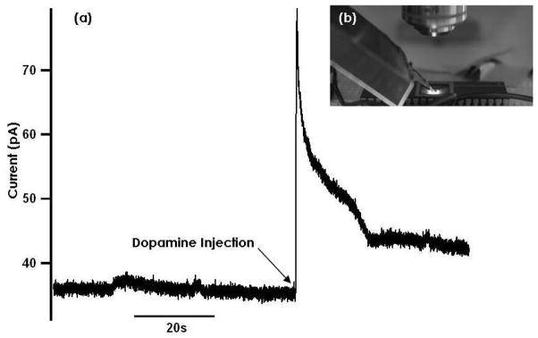
To demonstrate on-chip detection of dopamine release, the exposed cavity of the chip (white box shown in Fig. 3b) was filled with ≈ 20 μL of bath solution. Glucose was not added to the bath solution for dopamine experiments. A micropipette containing bath solution supplemented with 50 μM dopamine was immersed and positioned over the electrodes (Fig. 6b). Using a picospritzer (Picospritzer III, Parker Hannifin Corp., Fairfield, NJ), small amounts of solution were ejected from the pipette onto the 12 μm ×20 μm Pt electrode. The Ag|AgCl reference electrode was located inside the ejection pipette. Ejection of dopamine solution produced a clear amperometric response to the dopamine ejection followed by a decay, presumably reflecting dilution by diffusion. The background current of ~40 pA before the pressure pulse was applied is similar to that measured with surface patterned Pt electrodes of similar area connected to external amplifiers (manuscript in preparation). The noise in this recording was dominated by a superimposed sawtooth waveform of ≈ 20 Hz frequency, that we noticed in some recordings during preparation of the manuscript after the set-up was dismantled and the origin of which thus remains unknown. The rms noise level, after subtracting the sawtooth waveform from the original trace shown in Fig. 6b, was 0.35 pA for an integration time of 0.4 ms. The electronic noise of the potentiostat (0.11 pA rms) [22] is thus a minor contribution to the measurement noise. Shot noise associated with a current I is given by
Fig. 6.
(a) Current trace recorded by ejecting 50 μM concentration dopamine onto the chip electrode (b) Experimental setup showing the solution filled pipette containing the ground electrode ejecting solution on the electrode.
| (1) |
where q is the value of the charge of an electron e0. However, for dopamine oxidation, the unit is twice that charge, 2e0, because two electrons are transferred for every detected dopamine molecule. The noise bandwidth Δf for an averaging time interval τ is Δf = 1/(2τ). In this recording, with τ = 400 μs, the rms noise current is given by
| (2) |
For a current of ~40 pA (Fig. 6), even assuming that all the background current has a valence of 2, the rms shot noise would only be 0.18 pA, which also represents a minor contribution to the total observed noise variance in the recording. The measured 0.35 pA noise level is, however, typical for amperometric recordings of catecholamines with ~200 μm2 Pt electrodes connected to a conventional low-noise amplifier (manuscript in preparation). The noise is therefore dominated by the thermal noise of the electrode-electrolyte interface [30].
B. On-Chip Cellular Release Measurements
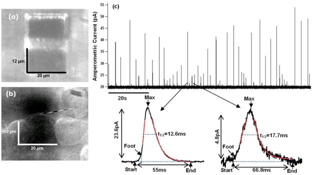
To demonstrate on-chip recording of single-release events, a pipette, approximately 100–200 μm in diameter, was filled with physiological saline containing suspended adrenal chromaffin cells and was positioned close to the electrodes, similar to the dopamine experiments described earlier. Gentle pressure was applied allowing the cells to move out of the pipette tip and settle randomly on the surface (Fig. 7b). To stimulate the cells, a small volume of a solution containing the calcium ionophore ionomycin at 20 μM concentration was added from a 10 μL pipette and amperometric currents were recorded. Most experiments showed no amperometric spikes, presumably due to cells not settling onto the recording electrode. However, amperometric spikes were recorded in a few successful experiments, as shown in Fig. 7c. The trace shows amperometric spikes as expected for a series of release events. Two events of different amplitudes are shown on expanded scale with peak currents of 23.6 pA and 4.8 pA, respectively. Event detection and analysis was performed automatically and the detection threshold for the events was set to 0.68 pA, four standard deviations of the average baseline current noise. For the two expanded events the fits for spike parameter determination are also shown in Fig. 7c. Statistical analysis of the 40 detected events revealed a median full width at half maximum of 12.8 ms and median peak current amplitude of 13.4 pA. These values are consistent with typical parameters of amperometric measurements of individual catecholamine release events from bovine chromaffin cells [4]–[6]. During the experiment, direct observation of cells through the microscope was difficult due to the curvature of the solution meniscus and the ionomycin application. However, these results suggest that a cell was presumably attached on or positioned very close to the electrode and that these events reflect single exocytotic events. However, in contrast to conventional carbon-fiber recordings, we observed few events which exhibited an extended pre-spike foot signals, which would normally be expected to occur among these events. An alternative possibility would be that the recorded events reflect release from vesicles that were liberated intact from damaged cells and which burst upon contact with the electrode. At this stage, we have demonstrated by proof of principle the feasibility of on-chip recording of single vesicle release events with high resolution.
Fig. 7.
(a) Microscope image of on-chip Pt electrode dimensions. (b) Bovine chromaffin cells dropped onto the chip surface. The image was taken for demonstration purposes only and not during actual experimentation. Cells were released onto the electrodes and a water immersion objective focused on the cells. In the background electrodes can be seen as dark shadow. (c) Amperometric current trace showing spikes of variable amplitude up to ≈ 55 pA. Two events on expanded scales with fit lines from the spike parameter analysis.
V. Conclusions
In this paper, we described the post-CMOS processing of CMOS chips to incorporate the transducer. We conclude that the layout floor plan must include considerations of the post-CMOS processing procedure. Photolithography is more desirable both for faster fabrication and for less damage to the electronics when large electrode arrays are processed. The results achieved with this process were variable because photoresist thickness was uneven across the die. However, complete coverage of the electrode with Ti/Au layer was obtained in some cases, as shown in Fig. 2b. Some of the patterning problems could be avoided by making the openings in the passivation layer larger than the Al pad area. Provisions including extra die area for handling and packaging the die, as well as placement of electrodes in the center of the die must be made to ensure high post-CMOS processing yield. We demonstrated the feasibility of on-chip recording of catecholamine release with high resolution. With this proof of concept, we envision building large-scale arrays. Furthermore, on large scale arrays, it is possible to treat the electrode areas with poly(D)-lysine to promote cell adhesion. This treatment would allow the cells to stick to the electrode during experimentation and provide high experimental yield.
Acknowledgments
We thank Dr. Qinghua Fang for preparing the cells, and Mr. Mick Thomas for assisting with the focused-electron-beam deposition of platinum. The CMOS chip was fabricated at MOSIS. Post-CMOS fabrication was performed at the Cornell Center for Materials Research (CCMR) and the Cornell Nanofabrication facility (CNF). This work was supported by the Nanobiotechnology Center (an STC program of NSF Agreement No. ECS-9876771) and by NIH (RO1 NS048826).
Biographies
 Sunitha Ayers recieved her B. Tech. degree in Electrical and Electronics Engineering with distinction from National Institute of Technology, Warangal, India (formerly known as Regional Engineering College) in May 2001. She received her M. Eng. degree in Electrical Engineering from Cornell University, Ithaca, NY, in August 2002. She recieved her Ph.D. degree in Electrical Engineering from Cornell University, Ithaca, NY, in January 2009. Her research interests include analog integrated circuit design and biomedical electronics.
 Khajak Berberian received a diploma in Electrical and Computer Engineering from the National Technical University of Athens, Greece in 2002. Following a brief internship at Olympus Optical Company, in Tokyo Japan, he joined the Ph.D. program of the Department of Biomedical Engineering at Cornell University. His research interests include developing micro- and nanoscale devices for biological and medical applications.
 Kevin D. Gillis Kevin D. Gillis received a B.S. degree in Electrical Engineering at Washington University in St. Louis in 1985. He also received a B.A. degree in Physics from St. Louis University that same year. He received M.S. and D.Sc. degrees from Washington University in 1988 and 1993, respectively, and received postdoctoral training at the Max Planck Institute for Biophysical Chemistry in Goettingen, Germany from 1993 – 1996. He is currently an Associate Professor in the Department of Biological Engineering and Department of Medical Pharmacology and Physiology, and an Investigator at the Dalton Cardiovascular Research Center at the University of Missouri, Columbia. His research interests include bioMEMS and use of biophysical assays to study the mechanisms of Ca2+-triggered exocytosis from cells.
 Manfred Lindau was trained as a physicist and received his doctorate from the Technical University of Berlin in 1983 in the field of Physical Chemistry. In 1988 he became Assistant Professor at the Free University of Berlin. From 1992 through 1997 he was an Associate Member of the Max-Planck-Institute for Medical Research and taught Biophysics at the University of Heidelberg. He joined the faculty at Cornell in 1997 where he is Professor of Applied and Engineering Physics and leads an interdisciplinary research group. Dr. Lindau has developed biophysical techniques for cell- and neurobiology including the first perforated patch recordings, improved cell-attached patch capacitance measurements, development of patch amperometry, and the first successful fabrication and application of surface-patterned amperometric electrode arrays. The central goal of his current research is to elucidate the mechanisms of exocytotic fusion and transmitter release. He is a Founding Member, Member of the Executive Committee and Program Coordinator of the Nanoscale Cell Biology Program at the Science and Technology Center for Nanobiotechnology at Cornell. He was elected as a Member of the Asian Institute of NanoBioScience and Technology. In 2003 he received a Research Award from the Alexander von Humboldt Foundation, Germany in recognition of his scientific achievements. He is active as a consultant in the areas of biophysics, physiology, and cell biology, and is a member of the Biophysical Society and the Society for Neuroscience.
 Bradley A. Minch received his B.S. degree in Electrical Engineering with distinction from Cornell University in May 1991. He received his Ph.D. degree in Computation and Neural Systems from the California Institute of Technology in June 1997. He is currently an Associate Professor of Electrical and Computer Engineering at the Franklin W. Olin College of Engineering in Needham, MA. From 1997 to 2004, he was an Assistant Professor in the School of Electrical and Computer Engineering at Cornell University. His research interests include low-voltage/low-power analog and digital integrated circuit design, translinear circuits, log-domain filters, and adaptive floating-gate MOS circuits. He received the IEEE Electron Devices Society’s Paul Rappaport Award in 1996. Dr. Minch is a member of the IEEE and of the Tau Beta Pi, Eta Kappa Nu, and Phi Kappa Phi honor societies.
Contributor Information
Sunitha Ayers, Email: sb288@cornell.edu, School of Electrical and Computer Engineering, Cornell University, Ithaca, NY.
Khajak Berberian, Email: knb6@cornell.edu, Department of Biomedical Engineering, Cornell University, Ithaca, NY.
Kevin D. Gillis, Email: gillisk@missouri.edu, Department of Biological Engineering, University of Missouri, Columbia, MO. NY
Manfred Lindau, Email: ml95@cornell.edu, School of Engineering and Applied Physics, Cornell University, Ithaca, NY.
Bradley A. Minch, Email: bradley.minch@olin.edu, Franklin W. Olin College of Engineering, Needham, MA.
References
- 1.Wightman RM, Jankowski JA, Kennedy RT, Kawagoe DT, Schroeder TJ, Leszczyszyn DJ, Near JA, Diliberto EJ, Jr, Viveros OH. Temporally resolved catecholamine spikes correspond to single vesicle release from individual chromaffin cells. Proceedings of the National Academy of Sciences of the United States of America; 1991. pp. 10754–10758. [DOI] [PMC free article] [PubMed] [Google Scholar]
- 2.Pothos E, Desmond M, Sulzer D. L-3,4-Dihydroxyphenylalanine increases the quantal size of exocytotic dopamine release in vitro. Journal of Neurochemistry. 1996;66:629–636. doi: 10.1046/j.1471-4159.1996.66020629.x. [DOI] [PubMed] [Google Scholar]
- 3.Pothos EN, Davila V, Sulzer D. Presynaptic recording of quanta from midbrain dopamine neurons and modulation of the quantal size. Journal of Neuroscience. 1998;18:4106–4118. doi: 10.1523/JNEUROSCI.18-11-04106.1998. [DOI] [PMC free article] [PubMed] [Google Scholar]
- 4.Gong LW, Alvarez De Toledo G, Lindau M. Secretory vesicles membrane area is regulated in tandem with quantal size in chromaffin cells. Journal of Neuroscience. 2003;23(21):7917–7921. doi: 10.1523/JNEUROSCI.23-21-07917.2003. [DOI] [PMC free article] [PubMed] [Google Scholar]
- 5.Chow RH, ‘Rden Lv, Neher E. Delay in vesicle fusion revealed by electrochemical monitoring of single secretory events in adrenal chromaffin cells. Nature. 1992;356:60–63. doi: 10.1038/356060a0. [DOI] [PubMed] [Google Scholar]
- 6.Albillos A, Dernick G, Horstmann H, Almers W, Alvarez de Toledo G, Lindau M. The Exocytotic Event in Chromaffin cells Revealed by Patch Amperometry. Nature. 1997;389:509–512. doi: 10.1038/39081. [DOI] [PubMed] [Google Scholar]
- 7.Colliver TL, Hess EJ, Pothos EN, Sulzer D, Ewing AG. Quantitative and statistical analysis of the shape of amperometric spikes recorded from two populations of cells. Journal of Neurochemistry. 2000;74:1086–1097. doi: 10.1046/j.1471-4159.2000.741086.x. [DOI] [PubMed] [Google Scholar]
- 8.Jenkner M, Tartagni M, Hierlemann A, Thewes R. Cell-based CMOS sensor and actuator arrays. IEEE Journal of Solid-State Circuits. 2004;39(12):2431–2437. [Google Scholar]
- 9.Eversmann B, Jenkner M, Hofmann F, Paulus C, Brederlow R, Holzapfl B, Fromherz P, Merz M, Brenner M, Schreiter M, Gabl R, Plehnert K, Steinhauser M, Eckstein G, Schmitt-Landsiedel D, Thewes R. A 128×128 CMOS biosensor array for extracellular recording of neural activity. IEEE Journal of Solid-State Circuits. 2003;38(12):2306–2317. [Google Scholar]
- 10.Schienle M, Paulus C, Frey A, Hofmann F, Holzapfl B, Schindler-Bauer P, Thewes R. A fully electronic DNA sensor with 128 positions and in-pixel A/D conversion. IEEE Journal of Solid-State Circuits. 2004;39(12):2438–2445. [Google Scholar]
- 11.Milgrew MJ, Riehle MO, Cumming DRS. A 16×16 CMOS Proton Camera Array for Direct Extracellular Imaging of Hydrogen-Ion Activity. Solid-State Circuits Conference, 2008. ISSCC 2008. Digest of Technical Papers. IEEE International; Feb, 2008. pp. 590–638. [Google Scholar]
- 12.Stanacevic M, Murari K, Thakor NV, Cauwenberghs G. VLSI Potentiostat Array With Oversampling Gain Modulation for Wide-Range Neurotransmitter Sensing. IEEE Transactions on Biomedical Circuits and Systems. 2007 March;1(1):63–72. doi: 10.1109/TBCAS.2007.893176. [DOI] [PubMed] [Google Scholar]
- 13.Narula HS, Harris JG. A Time-Based VLSI Potentiostat for Ion Current Measurements. IEEE Sensors Journal. 2006 April;2:239–247. [Google Scholar]
- 14.Narula HS, Harris JG. Integrated VLSI Potentiostat for Cyclic Voltammetry in Electrolytic Reactions. Proceedings of the IEEE Computer Society Annual Symposium on VLSI Emerging Trends in VLSI Systems Design (ISVLSI’04); 2004. pp. 268–270. [Google Scholar]
- 15.Genov R, Stanacevic M, Naware M, Cauwenberghs G, Thakor NV. 16-Channel Integrated Potentiostat for Distributed Neurochemical Sensing. IEEE Transactions on Circuits and Systems I: Regular Papers. 2006;53(11):2371–2376. [Google Scholar]
- 16.Murari K, Stanacevic M, Thakor NV, Cauwenberghs G. Wide-range, Picoampere-Sensitivity Multichannel VLSI Potentiostat for Neurotransmitter Sensing. Proceeding of the 26th Annual International Conference of the IEEE EMBS; San Francisco, CA: 2004. pp. 4063–4066. [DOI] [PubMed] [Google Scholar]
- 17.Laiwalla F, Klemic KG, Sigworth FJ, Culurciello E. An Integrated Patch-Clamp Amplifier in Silicon-on-Sapphire CMOS. IEEE Transactions on Circuits and Systems I: Regular Papers. 2006;53(11):2364–2370. [Google Scholar]
- 18.Roham M, Halpern JM, Martin HB, Chiel HJ, Mohseni P. Wireless amperometric neurochemical monitoring using an integrated telemetry circuit. IEEE Transactions on Biomedical Engineering. 2008;55(11):2628–2634. doi: 10.1109/TBME.2008.2001264. [DOI] [PMC free article] [PubMed] [Google Scholar]
- 19.Roham M, Garris PA, Mohseni P. A Wireless IC for Time-Share Chemical and Electrical Neural Recording. Dig. Tech. Papers IEEE Int. Solid State Circuits Conf. ISSCC’09; San Francisco, CA. February 8–12, 2009.pp. 430–431. [Google Scholar]
- 20.Roham M, Daberkow DP, Ramsson ES, Covey DP, Pakdeeronachit S, Garris PA, Mohseni P. A Wireless IC for Wide-Range Neurochemical Monitoring Using Amperometry and Fast-Scan Cyclic Voltammetry. IEEETransactions on Biomedical Circuits and Systems. 2008;2(1):3–9. doi: 10.1109/TBCAS.2008.918282. [DOI] [PubMed] [Google Scholar]
- 21.Hassibi A, Lee TH. A Programmable 0.18um CMOS Electrochemical Sensor Microarray for Biomolecular Detection. Proceeding of IEEE Sensors Journal. 2006;6(6):1380–1388. [Google Scholar]
- 22.Ayers S, Gillis KD, Lindau M, Minch BA. Design of a CMOS potentiostat circuit for electrochemical detector arrays. IEEE Transactions on Circuits and Systems I-Regular Papers. 2007;54(4):736–744. doi: 10.1109/TCSI.2006.888777. [DOI] [PMC free article] [PubMed] [Google Scholar]
- 23.Levine PM, Gong P, Levicky R, Shepard KL. Active CMOS Sensor Array for electrochemical biomolecular detection. IEEE Journal of Solid State Circuits. 2008;43(8):1859–1871. [Google Scholar]
- 24.Parsons TD, Coorssen JR, Horstmann H, Almers W. Docked granules, the exocytic burst, and the need for ATP hyd rolysis in endocrine cells. Neuron. 1995;15:1085–1096. doi: 10.1016/0896-6273(95)90097-7. [DOI] [PubMed] [Google Scholar]
- 25.Crow DR. Principles and applications of electrochemistry. New York: Blackie Academic & Professional; 1994. [Google Scholar]
- 26.Chow CH, Ruden . In: Single Channel Recording. Sakmann B, Neher E, editors. New York: Plenum Press; 1995. [Google Scholar]
- 27.Giannuzzi Lucille A, Stevie FA. Introduction to focused ion beams : instrumentation, theory, techniques, and practice. New York: Springer; 2005. [Google Scholar]
- 28.Mosharov EV, Sulzer D. Analysis of exocytotic events recorded by amperometry. Nat Methods. 2005;2:651–658. doi: 10.1038/nmeth782. [DOI] [PubMed] [Google Scholar]
- 29.Gong LW, Alvarez de Toledo G, Lindau M. Exocytotic catecholamine release is not associated with cation flux through channels in the vesicle membrane Na+ influx through the fusion pore. Nature Cell Biology. 9:915–922. doi: 10.1038/ncb1617. [DOI] [PMC free article] [PubMed] [Google Scholar]
- 30.Hassibi A, Navid R, Dutton RW, Lee TH. Comprehensive study of noise processes in electrode electrolyte interfaces. Journal of Applied Physics. 2004;96:1074–1082. [Google Scholar]


