Abstract
High-throughput electrode arrays are required for advancing devices for testing the effect of drugs on cellular function. In this paper, we present design criteria for a potentiostat circuit that is capable of measuring transient amperometric oxidation currents at the surface of an electrode with submillisecond time resolution and picoampere current resolution. The potentiostat is a regulated cascode stage in which a high-gain amplifier maintains the electrode voltage through a negative feedback loop. The potentiostat uses a new shared amplifier structure in which all of the amplifiers in a given row of detectors share a common half circuit permitting us to use fewer transistors per detector. We also present measurements from a test chip that was fabricated in a 0.5-μm, 5-V CMOS process through MOSIS. Each detector occupied a layout area of 35μm × 15μm and contained eight transistors and a 50-fF integrating capacitor. The rms current noise at 2kHz bandwidth is ≈ 110fA. The maximum charge storage capacity at 2kHz is 1.26 × 10⁶ electrons.
I. Introduction
NEURONAL function and behavior is determined, among other mechanisms, by the storage and release of neurotransmitters and hormones. The release of these substances, which are synthesized in the cytosol, occurs by a process of exocytosis, in which a secretory vesicle fuses with the plasma membrane. When an excitable cell is stimulated, the contents of one or more vesicles are released completely into the extracellular space. Release from a single vesicle has been termed quantal release. The current widespread interest in understanding the process of quantal release is motivated by its importance in human health and disease. Present-day techniques used to study quantal release include carbon-fiber amperometry [1], patch amperometry [2], and amperometry using microfabricated planar microelectrodes [3]. These amperometric techniques can detect quantal release of oxidizable transmitters, such as the catecholamines epinephrine and norepinephrine, using a carbon fiber or platinum microelectrode that is positioned close to the cell surface and held at a potential that is sufficiently high to oxidize the released molecules. Upon release from a vesicle, the catecholamine molecules that diffuse to the surface of the electrode are rapidly oxidized, resulting in the transfer of two electrons to the electrode [4]. The oxidation of the molecules released in a single quantal event thus generates a transient oxidation current with a duration of a few milliseconds. By integrating the transient signal, we can determine the number of molecules released and, thus, the quantal size. To understand properties of quantal events and to advance the study of their modulation by drugs, we need to develop high-throughput techniques that allow us to perform measurements of many quantal events from a large number of cells under a variety of experimental conditions.
In this paper, we describe the design of a new CMOS electrochemical detector array for high-throughput characterization of quantal events. The detector array comprises a two-dimensional array of electrodes, each of which is connected to a novel regulated cascode amplifier (RCA). To achieve cellular dimensions, each detector unit should be on the order of 10-20 μm on a side, which constrains the number of transistors per detector. The electrode potential must be stable, because an unstable electrode voltage leads to charging and discharging of the liquid junction capacitance creating excessive baseline fluctuations in current measurement. The half-width of the release events is typically a few milliseconds, which implies that the readout rate should be at least in the kHz range. The amperometric spikes are often preceded by a small foot signal of a few picoamperes in amplitude [5] that contains valuable information on the properties of the fusion pore [6]; this consideration implies that the input-referred noise current of a potentiostat detector should be less than 1pA. Some CMOS potentiostat designs have been proposed earlier [7], [8]. These designs employ current mirrors to amplify currents to the μA range, increasing power consumption. The RCA detector array is capable of measuring small currents without increasing the power consumption and layout area by eliminating amplifying circuitry. An approach discussed in [9] involves a pMOS, nMOS OTA and a dual slope comparator. Recently, time-base VLSI potentiostats [10–12], were proposed. These designs employ a pF integration capacitor and an OTA that occupies a large area. With our shared amplifier stage, we achieve similar performance while maintaining a small area. Previously, some proposed multichannel potentiostat circuits [13]. In these designs a standard differential amplifier is used to keep the potential of the electrode constant, while the readout is done using a a current-mode sigma-delta ADC with a variable oversampling ratio. While these designs are suitable for a small array, our design achieves better spatial resolution with the shared amplifier structure.
In this paper, we describe the design and implementation of the RCA potentiostat and report experimental results from a small test array that was fabricated in a 0.5-μm, 5-V CMOS process through MOSIS. In Section II, we explain the circuit operation. In Section III, we derive the noise analysis and compare the performance of our amplifier with that of a folded cascode amplifier. In Section IV, we present the schematics and operation of the output stage. In Section V, we show the measurement results. Finally in Section VI, we summarize the theory and experimental results.
II. Circuit Operation
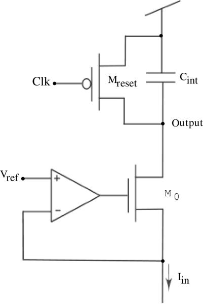
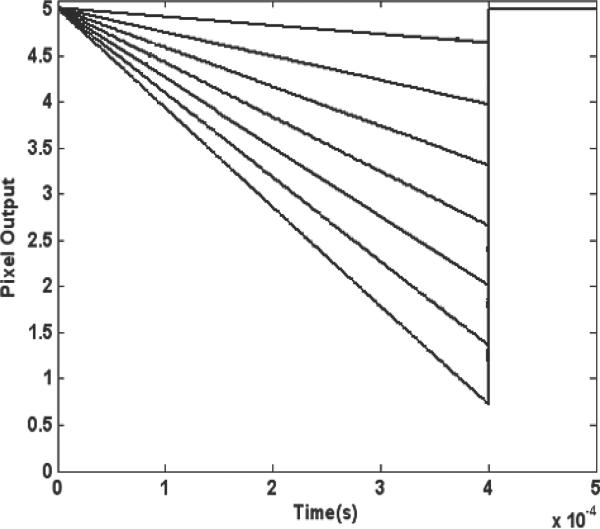
Figure 1 shows a schematic of a single potentiostat detector circuit. The circuit comprises a cascode transistor and a feedback amplifier that maintains the electrode at a stable reference voltage, Vref. The operation of the potentiostat is straightforward. The current Iin, produced as a result of oxidation events on the electrode surface, is buffered by the cascode transistor to the node labeled “Output” where it is integrated by a 50-fF integration capacitor, Cint, to produce an output voltage. Periodically, the output voltage is reset to the positive power supply rail, Vdd, through a reset transistor, Mreset. Figure 2 shows simulation results of the potentiostat for an integration time of 400μs. As we vary the input current from 50pA to 650pA in 100pA increments, the output voltage varies linearly with the input current. The input impedance of the cascode, gs0, is relatively low. When we add a high-gain amplifier, as shown in Fig. 1, to produce a regulated cascode, the input impedance is further reduced by the gain of the amplifier. In this application, we require low input impedance in order to maintain a high injection efficiency. Injection efficiency is defined as the fraction of the electrode current that is buffered by the cascode transistor to the output node. We can show that the low-frequency input impedance of the potentiostat is given by,
| (1) |
where gs0 is the incremental source conductance of the cascode transistor M0, κ is the reciprocal subthreshold slope factor, a constant with a typical value between 0.5-0.9, and A0 is the low-frequency gain of the regulation amplifier. For a typical input current level of tens to hundreds of picoamperes, this input resistance can be as low as hundreds to tens of kiloohms, which is much less than the impedance of the effective shunt capacitance formed at the liquid-solid interface of the electrode over the frequency range of interest, resulting in a very high injection efficiency.
Fig. 1.
Schematic view of a potentiostat circuit comprising the integration capacitor Cint, the feedback amplifier and reset switch Mreset.
Fig. 2.
Simulation results of the RCA circuit. The output voltage varies linearly with various input current values.
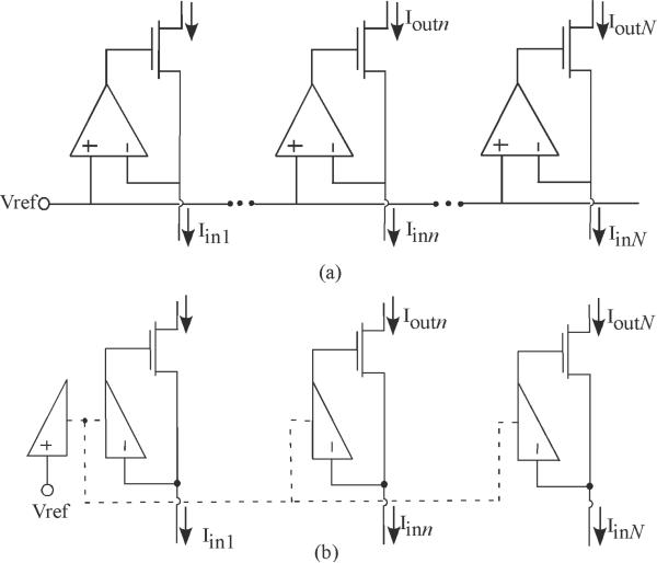
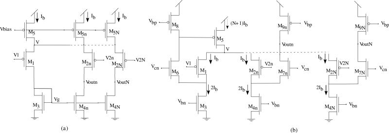
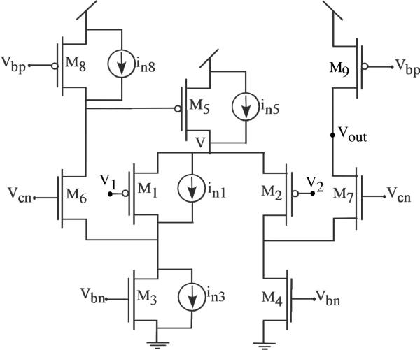
In order to keep each detector as small as possible, we used a shared amplifier structure in which all regulation amplifiers in a given row share a common half circuit. Figure 3a shows a one-dimensional array of regulated cascode circuits, in which each regulated cascode circuit has its own amplifier. However, because the noninverting input of each op-amp in the array is connected to a common potential, Vref, we can share a common half circuit among all of the amplifiers in the array, as shown conceptually in Fig. 3b. In this scheme, each amplifier requires only half the layout area and half the power consumption as would its counterpart in the array of Fig. 3a for a given unity-gain bandwidth and low-frequency gain. Such a scheme has been employed successfully in infrared imaging systems, in which context it is called share-buffered direct injection(SBDI) [14–16]. The shared half amplifier in the SBDI circuit, shown in Fig. 4a, comprises of transistors M1, M3, M5. The independent half circuits comprise of transistors M2n, M4n, M5n, where n ranges from 1 to N. We have designed a new shared amplifier circuit, shown in Fig. 4b, that is based on the folded-cascode op-amp topology.
Fig. 3.
An array of regulated cascode circuits (a) with independent op-amp circuits and (b) with the proposed scheme in which all amplifiers share a common half circuit.
Fig. 4.
Transistor-level schematics of (a)SBDI circuit proposed by Wu and Hsieh [14–16] (b) the proposed scheme in which we share a common half circuit (i.e., stage 1), between all of the amplifiers (i.e., amplifiers n and N shown) in the array shown in Fig. 3b.
Figure 4b shows a transistor-level schematic of the shared amplifier circuit. The shared half circuit (i.e., stage 1, shown on the left in Fig. 4b) comprises M1, M3, M5, M6, and M8. N independent half circuits are added to stage 1 at the node V. The nth independent half circuit (i.e., stage n) comprises M2n, M4n, M7n, and M9n, where n ranges from 1 to N. To generate the bias voltages Vbp, Vcn and Vbn, we use a low-voltage cascode bias circuit that we have previously described [17]. The shared half circuit contains a negative feedback loop that maintains V just far enough above the common noninverting input voltage, V1, so that transistor M1 passes the bias current, Ib.
The operation of a single amplifier is described here by considering the shared half circuit, stage 1, and the independent half circuit, stage n. If the inverting input voltage to stage n, V2n, is equal to V1, then transistor M2n, which is nominally identical to M1, also passes Ib. Consequently, by Kirchhoff's current law (KCL), transistor M7n will also pass Ib, which matches the saturation current of M9n, so the amplifier will be in its high-gain region in which M7n and M9n are both saturated. If V2n is slightly below V1, then transistor M2n will pass substantially more current than Ib, reducing the current flowing in M7n causing Voutn to rise until M9n is in its ohmic region. On the other hand, if V2n is slightly above V1, then transistor M2n will pass substantially less current than Ib, increasing the current flowing in M7n causing Voutn to fall until M7n is in its ohmic region. In a small range of voltages around the point at which, V1 ≈ V2n we can show that the incremental output voltage of the shared amplifier is given by,
| (2) |
where A0 is the low-frequency gain of the amplifier, gm2n is the incremental transconductance gain of each input transistor M2n, and ro9n is the incremental output resistance of the pMOS transistor M9n.
Next, we describe feedback regulation of node V by the N amplifiers that share the common half circuit. If the inverting voltages V22-V2N = V1, then the inverting input transistors M22-M2N, that are equivalent to M1 also pass a current of Ib. According to KCL,
| (3) |
The feedback loop adjusts the gate voltage of M5 to pass a current of (N + 1) Ib and the common node V just enough to allow M1 to pass Ib. The capacitance at node V is the sum of the N source capacitances contributed by N input stages. Thus the capacitive load on node V is proportional to N. However, from (3), the bias current of M5 is also proportional to N.
Our new shared amplifier represents an improvement over the SBDI circuit, in terms of low-frequency gain, the shared half circuit's ability to drive the capacitive load imposed by the common line V, that couples the amplifiers together and stability, isolation between neighboring amplifiers and each amplifier's output swing. We shall discuss each of these improvements in turn in the following subsections.
A. Low Frequency Gain
The low frequency gain of our amplifier is given by gm2ro9. The output impedance and the transconductance gain are provided by different transistors M9 and M2 respectively. We can optimize the gain of our amplifier by making the transistor M9 longer. The gain of the RCA circuit is a 6dB improvement over the gain of the SBDI amplifier [14–16], which is gm2(ro2 ∥ ro4), provided the output impedance of the pMOS and nMOS transistors are comparable. In this circuit, the transconductance gain and the output impedance depend on the same transistor M2. gm2 and ro2 trade off with each other which would make it difficult to optimize the gain.
B. Stability and Bandwidth
The negative feedback loop also greatly reduces the incremental resistance through which the half circuit drives node V. We can show that the incremental resistance seen looking back into the shared half circuit, stage 1, is given by,
| (4) |
Analysis of the frequency response of the RCA reveals that the nondominant pole of the amplifier is at node V. The nondominant pole is [RVCV]−1, where CV is the total capacitance at node V . Due to the reduced impedance given in (6), the nondominant pole is pushed farther away from the dominant pole, by the gain (1 + gm5ro8), providing wider bandwidth and stability.
C. Isolation between amplifiers
When there is an incremental change in the input voltage of stage n, δV2n, and stage (n + 1), δV2(n+1), an incremental current gm2nδV2n, gm2nδV2(n+1) flows through M7n and M7(n+1) respectively, changing their output voltages. The incremental output voltages of stages n and (n + 1) are,
| (5) |
| (6) |
The outputs δVoutn and δVout(n+1) are only dependent on their own input voltages. The node V remains unchanged so long as the noninverting input V1 is held constant. The gain from node V to each output of the circuit of Fig. 4a is gs2(ro2 ∥ ro4) and to each output of the circuit of Fig. 4b is gs2ro9. Any movement of node V induced by the inverting input of one amplifier would couple into the other outputs. In our circuit, the common source line, V , is better regulated by the negative feedback loop, which lowers the effective resistance through which V is driven by a factor of gm5ro8.
D. Output Swing
Many applications require us to vary the reference voltage to observe redox currents at the electrode surface. With our shared amplifier scheme, we can set the potential of the electrode anywhere in the range of 0 V to 3.2 V, which may be required in such applications. The output swing of the amplifier is an improvement over [14–16], extending from two saturation voltage drops above ground to one saturation voltage drop short of Vdd. In subthreshold, the saturation voltage drop is approximately 100-130mV, which translates to an almost rail-to-rail output voltage swing. The SBDI circuit was used to regulate the source of a pMOS transistor. If this amplifier was used to regulate an nMOS transistor, as shown in Fig. 1, we would use a complementary version of the shared amplifier. In that case for transistor M2n to remain in saturation, the output voltage has to be substantially higher than the inverting input voltage. This means that the regulated electrode node can have a limited range of voltages or that the power supply voltage has to be increased by 1.2-1.5V. The RCA circuit can regulate both pMOS and nMOS transistors without loosing output swing.
These improvements over the SBDI circuit come at the cost of power consumption. The power consumption of each RCA unit is 2IbVdd as compared to IbVdd of the SBDI unit. This scheme allows us to achieve a performance similar to the folded-cascode amplifier at a cost of fewer than half the number of transistors in each potentiostat. The amplifier can have a low-frequency gain in the thousands and effectively maintain a stable reference voltage at each electrode.
III. Noise Analysis
The noise performance of our amplifier is comparable to that of a folded-cascode amplifier, for a given bias level and set of transistor dimensions. The thermal noise sources corresponding to each transistor of our amplifier are shown in Fig. 5. The folded cascode amplifier shown in Fig. 4a has similar noise sources associated with each corresponding transistor. These sources represent the thermal current noise per unit bandwidth of a subthreshold MOS transistor, the variance of which is given by [20], [21],
| (7) |
where the transconductance gm = κID/UT and κ is the reciprocal subthreshold slope factor. The right half of our amplifier is similar to that of a regular folded cascode amplifier, resulting in the same effect by each corresponding transistor on the output node. We can show that the corresponding transistors in the left half of the amplifiers have a similar effect on their output nodes. The noise current source in5 of the folded cascode amplifier in Fig. 4a flows symmetrically through the two paths and cancels at the output node. In our amplifier, the source in5 sees a current divider between the two paths. The output thermal noise contribution of transistor M5 is ino5, given by,
For typical bias currents, the loop gain . Further, when we share the amplifier among N pixels in a row gm5ro8 is larger. Since gm5 is proportional to bias current, which is (N + 1) Ib, the loop gain gm5ro8 is increased N-fold. The increase in gm5 also leads to an N-fold increase in the noise current source in5. However, the resulting noise current is shared by N half-amplifiers contributing negligible noise currents to each amplifier's output. Thus, we can conclude that ino5 is negligible. The noise sources in8 and in3 in Fig. 4a are mirrored to the output node. In our amplifier, the effect of in8 on the output is
Similarly the effect of M3 is,
A complete noise analysis revealed that the total input referred voltage noise per unit bandwidth, is,
| (8) |
The input referred noise is approximately equal to that of a folded cascode amplifier, although in our scheme, the amplifier occupies half the layout area and consumes half the power per amplifier.
Fig. 5.
Schematic of the amplifier with equivalent thermal noise current sources in1, in3, in5, in8 of the transistors M1, M3, M5, M8, that contribute to the output.
Flicker (or 1/f) noise is an important consideration in low-frequency measurements. In most CMOS technologies, pMOS transistors have one or two orders of magnitude lower 1/f noise than do nMOS transistors [22]. In our amplifier, by using pMOS input transistors, we reduced the 1/f noise. Flicker noise is inversely proportional to the gate area. Maximizing the area of the transistors, however, would increase the pitch. Here, the choice of minimum width transistors degraded the 1/f noise. We further reduce the 1/f noise by using a correlated double sampling circuit [23], [24], described in the following section.
In addition to the noise contributed by the feedback amplifier, the reset transistor Mreset contributes noise due to clock feedthrough, charge injection and thermal noise of the on-resistance of the reset switch. When the signal goes from on to off i.e. from low to high, the clock signal feeds through the gate-drain capacitance Cgd, and appears across the integration capacitance Cint. The clock feedthrough is quantified as,
| (9) |
Another form of noise due to the reset transistor is charge injection. When the switch is turned off, the charge under the gate oxide is injected into the integration capacitor. However, these effects are offsets and can be corrected through calibration and double sampling. The on-resistance of the switch introduces thermal noise on the output node and when the switch is turned off, this noise is sampled onto the integration capacitor. This noise scales as,
| (10) |
It can be reduced by increasing the integrating capacitor which would also increase the layout area and decrease the transimpedance gain for a given switching frequency. We have to optimize the size of the integration capacitor considering the trade off between noise, layout area, frequency and gain.
IV. Output Stage
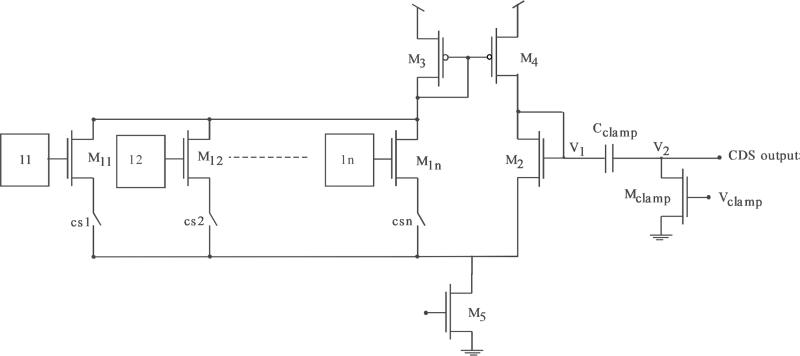
The source follower, which is used to buffer the detector output to the readout circuitry in infrared imagers and active pixel sensors [16], [18], [19], suffers from many shortcomings. The source follower has limited output voltage swing. The gain of the source follower is κ, which has a dependence on its input voltage, so the source follower is nonlinear. The temperature dependance of κ and the back-gate effect also degrade the gain. However, the source follower is widely used because of its simplicity and smaller layout area. In our scheme, we use an almost rail-to-rail differential amplifier, that has uniform gain of unity across the chip. The schematic of the first row of potentiostat detector circuits and the common output stage is shown in Fig. 6. The buffer is shared by all the detectors in a row. The detectors 11 through 1n are sequentially switched to complete the buffer by turning on the column switches cs1 through csn. The noninverting input and the access switch are a part of the detector, while the remaining transistors are outside the detector. By using this architecture, we achieve better performance than the source follower without paying in terms of layout area. This kind of architecture is used in active pixel imagers for high speed readout [25]. The buffered output is then fed to the correlated-double sampling (CDS) circuit shown in Fig. 6. At the end of the integration period, Mclamp and cs1 are closed, and the node V1 is set to a voltage of (Vdd − Vsig + Vn), where Vsig the output voltage of potentiostat11, and Vn is the 1/f noise. During this time, V2 is held at ground by Mclamp. At reset, when the integrating capacitor Cint is reset to Vdd, the switch Mclamp is opened pulling V1 to (Vdd + Vn). The voltage V2 is the difference of the two samples, (Vdd + Vn) − (Vdd − Vsig + Vn)=Vsig, which is buffered onto a multiplexed common bus. The CDS circuit thus reduces the 1/f noise.
Fig. 6.
Schematic block diagram of the common output stage,where an output stage of row1 is shared by n columns. Each column is sequentially switched through cs1,...csn to the output buffer to sample the output at the end of the integration period.
V. Results
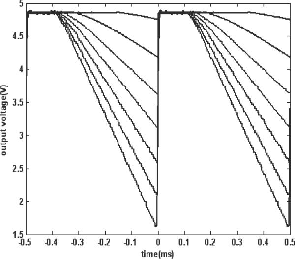
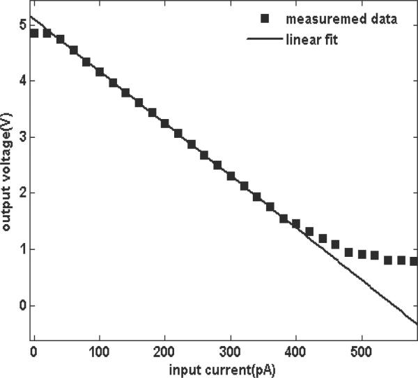
We fabricated a test chip containing a 5 × 5 detector array in a 0.5-μm, 5-V CMOS process through×MOSIS in order to verify the basic operation of the detector and the shared amplifier circuit technique, shown in Fig 7. The area of a single detector was 525 μm2 and the pitch was 15 μm. Figure 8 shows the test results from a single detector. Each unit contained a 50-fF integration capacitor. We set the amplifier bias current to 100 nA for these measurements. The power consumption of each unit is 1μW. For these tests, we supplied the input current through an nMOS current mirror. We varied the input current from 10 pA-600 pA and used an integration time of 400 μs. Throughout, we held the reference voltage constant at 0.7 V, which is a typical electrode potential for amperometric experiments. It should be noted that the output voltage does not extend all the way to the positive supply rail, because it was buffered by an amplifier whose maximum output voltage was 4.85 V. Thus for the smallest input currents, the final output voltage is not discernable. A rail-to-rail buffer design would make measuring small currents possible. As the input current increases, the final output voltage increases linearly. With a 50-fF integration capacitor and a 400-μs integration time, the output voltage saturates at about 0.8 V for an input current of 500 pA. An improved buffer design will make it possible to record smaller currents down to the noise limit, such a design is required to record amperometric foot signals. Figure 9 shows the current-voltage characteristic of a unit detector after the correlated double sampling circuit. The fit and the measured data are in good agreement verifying the linear behavior of the potentiostat. The transimpedance gain of the potentiostat detector is 9.3mV/pA. The coefficient of determination of the current-voltage characteristic is 0.99 in the current range of 20pA-400pA.
Fig. 7.
Micrograph of the die showing the 5x5 array of electrodes. The electrodes are 10μ on each side.The area enclosed by the solid lines is a single potentiostat circuit.
Fig. 8.
Measurement results showing the output voltage of the unit potentiostat for two clock periods.
Fig. 9.
I-V characteristic of the potentiostat, showing a linear behavior. Here the input current is varied from 10pA to 600pA and an integration capacitance of 50fF was used.
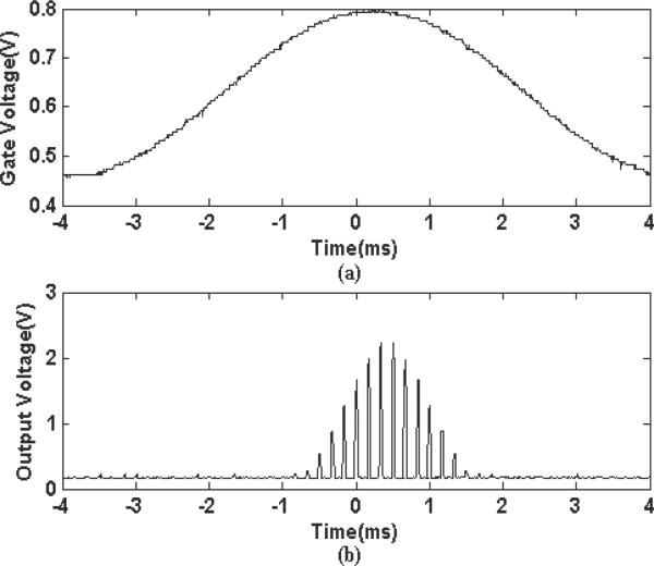
The charge resolution is set by the noise. The noise at the output of the detector, for measurements at input current of 20pA is shown in Fig 10. The figure shows thousand superimposed measurements of the output voltage. The rms noise of the measurements is ≈ 110fA or 274 electrons. The maximum charge storage capacity is approximately 1.26 × 10⁶ electrons. Current commercially available amplifiers used for amperometry include the VA10 (NPI Electronics), which specifies current noise less than 1pA as well as the high-end low-noise patch clamp amplifiers EPC7/8 (HEKA Electronics) and Axopatch 200B (Molecular Devices). For the EPC7/8 noise less than 0.1 pA is specified at 3 kHz bandwidth, which is close to the 0.11 pA at 2 kHz bandwidth of our circuit. The lowest noise is achieved by the Axopatch 200B (0.06 pA at 5 kHz). Our circuit uses very few components and incorporates a scalable array of amplifiers and compares overall favorably with current state-of-the-art instruments. Based on the circuit design we expect that the noise performance of our circuit may be optimized eventually approaching that of the Axopatch 200B amplifier. Figure 11 shows the output of the CDS circuit of a single detector in the prototype 5x5 array. Here again, the CDS output is seen to vary linearly with the input current. The transimpedance gain of the detector circuit after the CDS stage is 9mV/pA. The I-V characteristic of the CDS output of several pixels in a row is shown in Fig 12. Experimental data and linear fit are in good agreement verifying linear operation. The mismatch between potentiostats in a row varied from 6%-14%. It is important to note that one of the factors that contributes to the mismatch is the use of current mirrors of minimum dimensions to inject current. Current mirrors would not be necessary in the electrochemical setup, which would reduce the mismatch. Dynamic current measurements are shown in Fig. 13. A slow moving sine wave is applied to the gate of the current mirror. At sampling frequency of 6kHz, the output follows the input voltage above the threshold voltage of the nMOS transistor.
Fig. 10.
Measured data showing the output noise of the potentiostat circuit for an input current of 20pA. The rms error is equivalent to 0.1095pA or 274electrons.
Fig. 11.
Measured data showing the output of the correlated double sampling circuit for an input current of 10pA-400pA.
Fig. 12.
Measured data showing the IV characteristic of several potentiostats after the correlated double sampling stage. The solid line indicates a linear fit of the data.
Fig. 13.
Measured data showing (a) The varying voltage applied to the gate of the current mirror. (b) The sampled output voltage.
VI. Summary
We presented the operation, simulation and test results of a new potentiostat unit, that would be used for measuring electrochemical currents to reveal neuronal function in a high-throughput array. The unit detector size was 35μm × 15μm, suitable for cellular dimensions. The input impedance of the circuit was in the range of kiloohms, providing high injection efficiency. We showed that the input referred noise of the regulation amplifier was similar to that of a regular folded cascode amplifier and the 1/f noise is reduced by employing a CDS circuit. A stable electrode bias provided by the regulation amplifier, can be varied over a range of 0-3.2V. These specifications makes the potentiostat a suitable candidate for many other applications including infrared imagers and active pixel sensors. The functionality of the potentiostat was simulated using T-SPICE and verified by measurements conducted on an experimental chip.
ACKNOWLEDGEMENTS
This work was supported by the Nanobiotechnology Center (an STC program of NSF Agreement No. ECS-9876771) and by NIH (RO1 NS048826).
Biography
 Sunitha Ayers recieved her B. Tech. degree in Electrical and Electronics Engineering with distinction from National Institute of Technology, Warangal, India (formerly known as Regional Engineering College) in 2001. She received her M. Eng. degree in Electrical Engineering from Cornell University, Ithaca, NY, in 2002. She is currently working towards the Ph.D. degree in Electrical Engineering at Cornell University. Her research interests include analog integrated circuit design and biomedical electronics.
 Kevin D. Gillis received a B.S. degree in Electrical Engineering at Washington University in St. Louis in 1985. He also received a B.A. degree in Physics from St. Louis University that same year. He received M.S. and D.Sc. degrees from Washington University in 1988 and 1993, respectively, and received postdoctoral training at the Max Planck Institute for Biophysical Chemistry in Goettingen, Germany from 1993 - 1996. He is currently an Associate Professor in the Department of Biological Engineering and Department of Medical Pharmacology and Physiology, and an Investigator at the Dalton Cardiovascular Research Center at the University of Missouri, Columbia. His research interests include bioMEMS and use of biophysical assays to study the mechanisms of Ca2+-triggered exocytosis from cells.
 Manfred Lindau was trained as a physicist and received his doctorate from the Technical University of Berlin in 1983 in the field of Physical Chemistry. In 1988 he became Assistant Professor at the Free University of Berlin. From 1992 through 1997 he was an Associate Member of the Max-Planck-Institute for Medical Research and taught Biophysics at the University of Heidelberg. He joined the faculty at Cornell in 1997 where he is Professor of Applied and Engineering Physics and leads an interdisciplinary research group. Dr. Lindau has developed biophysical techniques for cell- and neurobiology including the first perforated patch recordings, improved cell-attached patch capacitance measurements, development of patch amperometry, and the first successful fabrication and application of surface-patterned amperometric electrode arrays. The central goal of his current research is to elucidate the mechanisms of exocytotic fusion and transmitter release. He is a Founding Member, Member of the Executive Committee and Program Coordinator of the Nanoscale Cell Biology Program at the Science and Technology Center for Nanobiotechnology at Cornell. He was elected as a Member of the Asian Institute of NanoBioScience and Technology. In 2003 he received a Research Award from the Alexander von Humboldt Foundation, Germany in recognition of his scientific achievements. He is active as a consultant in the areas of biophysics, physiology, and cell biology, and is a member of the Biophysical Society and the Society for Neuroscience.
 Bradley A. Minch received his B.S. degree in Electrical Engineering with distinction from Cornell University in May 1991. He received his Ph.D. degree in Computation and Neural Systems from the California Institute of Technology in June 1997. He is currently an Associate Professor of Electrical and Computer Engineering at the Franklin W. Olin College of Engineering in Needham, MA. From 1997 to 2004, he was an Assistant Professor in the School of Electrical and Computer Engineering at Cornell University. His research interests include low-voltage/low-power analog and digital integrated circuit design, translinear circuits, log-domain filters, and adaptive floating-gate MOS circuits. He received the IEEE Electron Devices Society's Paul Rappaport Award in 1996. Dr. Minch is a member of the IEEE and of the Tau Beta Pi, Eta Kappa Nu, and Phi Kappa Phi honor societies.
Contributor Information
Sunitha Ayers, School of Electrical and Computer Engineering, Cornell University, Ithaca, NY. sb288@cornell.edu..
Kevin D. Gillis, University of Missouri, Columbia, MO. gillisk@missouri.edu.
Manfred Lindau, School of Engineering and Applied Physics, Cornell University, Ithaca, NY. ml95@cornell.edu..
Bradley A. Minch, Franklin W. Olin College of Engineering, Needham, MA. bradley.minch@olin.edu..
References
- 1.Chow CH, Rüden . In: Single Channel Recording. Sakmann B, Neher E, editors. Plenum Press; New York: 1995. pp. 245–275. [Google Scholar]
- 2.Dernick G, Gong LW, Tabares L, Alvarez de Toledo G, Lindau M. Patch Amperometry: High-Resolution Measurements of Single-Vesicle Fusion and Release. Nature Methods. 2005;2(9):699–708. doi: 10.1038/nmeth0905-699. [DOI] [PubMed] [Google Scholar]
- 3.Hafez I, Kisler K, Berberian K, Dernick G, Valero V, Young MG, Craighead HG, Lindau M. Electrochemical Imaging of Fusion Pore Openings by Electrochemical Detector Arrays. Proceedings of the National Academy of Sciences, USA. 2005;102(39):13879–13884. doi: 10.1073/pnas.0504098102. [DOI] [PMC free article] [PubMed] [Google Scholar]
- 4.Baur JE, Kristensen EW, May LJ, Wiedemann DJ, Wightman RM. Fast-Scan Voltammetry of Biogenic Amines. Anal Chem. 1988;60(13):1268–1272. doi: 10.1021/ac00164a006. [DOI] [PubMed] [Google Scholar]
- 5.Chow RH, Rüden LV, Neher E. Delay in Vesicle Fusion Revealed by Electrochemical Monitoring of Single Secretory Events in Adrenal Chromaffin Cells. Nature. 1992;356:60–63. doi: 10.1038/356060a0. [DOI] [PubMed] [Google Scholar]
- 6.Albillos A, Dernick G, Horstmann H, Almers W, Alvarez de Toledo G, Lindau M. The Exocytotic Event in Chromaffin cells Revealed by Patch Amperometry. Nature. 1997;389:509–512. doi: 10.1038/39081. [DOI] [PubMed] [Google Scholar]
- 7.Turne RFB, Harrison DJ, Baltes HP. A CMOS Potentiostat for Amperometric Chemical Sensors. IEEE Journal of Solid-State Circuits. 1987;SC-22(3):473–478. [Google Scholar]
- 8.Bandopadhyay A, Mulliken G, Cauwenberghs G, Thakor NV. VLSIpotentiostat Array for Distributed Electrochemical Neural Recording. Pro-ceedings of IEEE International Symposium on Circuits and Systems; Phoenix,AZ. 2002. pp. II-740–II-743. [Google Scholar]
- 9.Breten M, Lehmann T, Braun E. Integrating Data Converters for Picoampere Currents from Electrochemical Sensors. Proceedings of the 2000 IEEE International Symposium on Circuits and Systems; Geneva, Switzerland. 2000. pp. 709–712. [Google Scholar]
- 10.Narula HS, Harris JG. VLSI Potentiostat for Amperometric Measurements for Electrolytic Reactions. Proceedings of the 2004 IEEE International Symposium on Circuits and Systems; Vancouver, Canada. 2004. pp. 457–460. [Google Scholar]
- 11.Narula HS, Harris JG. A Time-Based VLSI Potentiostat for Ion Current Measurements. IEEE Sensors Journal. 2006 April;2:239247. [Google Scholar]
- 12.Narula HS, Harris JG. Integrated VLSI Potentiostat for Cyclic Voltammetry in Electrolytic Reactions; Proceedings of the IEEE Computer Society Annual Symposium on VLSI Emerging Trends in VLSI Systems Design (ISVLSI'04); 2004. pp. 268–270. [Google Scholar]
- 13.Murari K, Stanacevic M, Thakor NV, Cauwenberghs G. Wide-range,Picoampere-Sensitivity Multichannel VLSI Potentiostat for Neurotransmitter Sensing. Proceeding of the 26th Annual International Conference of the IEEE EMBS; San Francisco, CA. 2004. pp. 4063–4066. [DOI] [PubMed] [Google Scholar]
- 14.Hsieh CC, Wu CY, Jih FW, Sun TP. Focal-Plane-Arrays and CMOS Readout Techniques of Infrared Imaging Systems. IEEE Transactions on Circuits and Systems for Video Technology. 1997;7:594–605. [Google Scholar]
- 15.Wu CY, Hsieh CC. New Design Techniques for a Complementary Metal-Oxide Semiconductor Current Readout Integrated Circuit for Infrared Detector Arrays. Optical Engineering. 1995;34:160–168. [Google Scholar]
- 16.Wu CY, Hsieh CC, Jih FW, Sun TP, Yang SJ. A New Share-Buffered Direct-Injection readout Structure for Infrared Detector Arrays. SPIE. 1993;2020:57–64. [Google Scholar]
- 17.Minch BA. A Low-Voltage MOS Cascode Bias Circuit for All Current Levels. IEEE International Symposium on Circuits and Systems. 2002;3:619–622. [Google Scholar]
- 18.Kulah H, Akin T. A Current Mirroring Integration Based Readout Circuit for High Performance Infrared FPA Applications. IEEE Transactions on Circuits and Systems-II:Analog and Digital Signal Processing. 2003;50(4):181–186. [Google Scholar]
- 19.Hsieh CC, Wu CY, Sun TP. A New Cryogenic CMOS Readout Structure for Infrared Focal Plane Array. IEEE Journal of Solid-State Circuits. 1997;32(8):1192–1199. [Google Scholar]
- 20.Sarpeshkar R, Delbruck T, Mead CA. White Noise in MOS Transistors and Resistors. IEEE Circuits and Devices. 1993;9(6):23–29. [Google Scholar]
- 21.Liu S-C, Kramer J, Indiveri G, Delbrck T, Douglas R. Analog VLSI Circuits and Principles. MIT Press; Cambridge, MA: 2002. pp. 313–340. [Google Scholar]
- 22.Jakobson C, Bloom I, Nemirovsky Y. 1/f Noise in CMOS Transistors for Analog Applications from Subthreshold to Saturation. Solid-State Electronics. 1998;42(10):1807–1817. [Google Scholar]
- 23.Kansy RJ. A Response of a Correlated Double Sampling Circuit to 1/f Noise. IEEE Journal of Solid-State Circuits. 1980;SC-15:373–375. [Google Scholar]
- 24.Wey HM, Guggenbühl W. An improved Correlated Double Sampling Circuit for Low Noise Charge-Couple Devices. IEEE Journal of Solid-State Circuits. 1990;37:1559–1565. [Google Scholar]
- 25.Boemler C, Zarnowski J. Image Sensor ADC and CDS per Column. 2005 US6965407 B2.


