

Abstract
A method for rapidly assembling high-density DNA arrays with near-perfect order is described. Photolithography is used to generate a wafer-scale array of microwells in a layer of photoresist on a chemically functionalized glass coverslip. The array is enclosed within a microfluidic device, and a suspension of superparamagnetic microbeads conjugated to DNA molecules is introduced into the chamber. A permanent magnet is used to direct the rapid assembly of the beads into the wells, with each well containing a single bead. These beads are immobilized on the glass surface via affinity binding, and excess beads can be recycled or washed away. Nonspecifically bound beads are removed by dissolving the photoresist. The result is a high-density array of beads with virtually no background. This method can be used to produce protein arrays for chip-based assays and DNA arrays for geno-typing or genome sequencing.
Some of the greatest breakthroughs in biomedical research can be attributed to the development of the numerous high-throughput technologies for quantitative measurements of biomolecules. Many of these technologies are made possible by microfabrication techniques commonly used in the semiconductor industry. For example, DNA and protein arrays fabricated by robotic printing and photolithographic methods have enabled extremely large-scale surveys of biomolecules.1–4 The emerging “next generation” genome sequencing technologies, many of which utilize massive parallelization and miniaturization to achieve unprecedented multiplexing, throughput and cost reductions,5–10 promise to revolutionize biomedical research and enable personalized healthcare. However, some of these technology platforms utilize randomly distributed DNA-conjugated microbeads or clones on a glass slide within a reaction chamber. The random arrangements of the beads or clones result in low throughput and imaging efficiency, complicated image processing, and high reagent costs.6–10 One approach to dramatically improve these devices involves the use of microfabricated arrays to eliminate overlap and to minimize the area between the beads or clones.
Such arrays can be generated by depositing samples onto glass slides using robotic contact printing,2 microcontact printing,11–13 or dip pen lithography.14 These arrays can also be generated by assembling beads onto microfabricated arrays of wells on glass or silicon substrates15–18 or in etched wells on the face of a fiber-optic bundle.19,20 Since bead assembly will not occur in an efficient and reliable manner if the process depends solely upon gravitational forces and Brownian motion, this process is typically achieved via solvent evaporation or dewetting.17–21 However, these approaches are not suitable when rapid assembly is required or sample drying is undesirable. Other groups have employed electric22 and magnetic23–25 assembly methods to overcome these issues, but these active approaches require multistep fabrication processes and complex field generation schemes. For many genomic and proteomic applications, the array fabrication and assembly processes need to be scalable and inexpensive. The format of the arrays must also be compatible with high-throughput imaging and microfluidic devices. Our approach satisfies these criteria by combining a single photolithographic step with the facilitated self-assembly of magnetic microbeads to create large, high-density DNA arrays on cover glass.
Our method for fabricating high-density biomolecular arrays is illustrated in Figure 1. The process begins with the silanization and biotinylation of the surface of a glass coverslip. Photolithography is then used to generate high-density arrays of micrometerto submicrometer-scale wells in a thin layer of photoresist that has been spin-coated on the glass surface. The patterned glass coverslip is enclosed within a flow cell, and a suspension of streptavidin-coated superparamagnetic microbeads conjugated to DNA molecules is introduced into the device. A permanent magnet is briefly dragged along the back side of the cover glass to direct the rapid assembly of the microbeads into the wells. The beads are immobilized in the wells via biotin–streptavidin affinity binding with only one bead fixed within each well due to physical constraints. Excess beads are washed away, and nonspecifically bound beads are removed by dissolving the photoresist with ethanol. The result is a high-density array of single beads with virtually no background.
Figure 1.

Rapid magnetic assembly of high-density DNA arrays. The schematic illustrates the steps involved in the fabrication and assembly process. The left panel shows the basic procedure, whereas the right panel illustrates the surface chemistry used to attach the beads to the array and the DNA to the beads. See text for a detailed description. The final microbead array is shown without the flow cell for illustrative purposes only. The drawing is not to scale.
EXPERIMENTAL SECTION
Chemical Derivatization of Glass Surfaces
The 50 × 75 × 0.170 mm3 borosilicate glass coverslips (Erie Scientific, Portsmouth, NH) were washed with a detergent solution and rinsed with 18 MΩ/cm deionized water. They were further cleaned by soaking in methanol and then acetone for 5 min each in an ultrasonic bath and dried in a convection oven at 110 °C for 10 min. The coverslips were then soaked in a 2 M nitric acid solution for 30 min at room temperature and rinsed with deionized water. Silanization was performed using a 2% solution of 3-aminopropyltriethoxysilane (Gelest Inc., Morrisville, PA) in 95:5 acetone/water for 15 min at room temperature. The coverslips were then rinsed three times with acetone and cured at 110 °C for 15 min in a convection oven. A 1 mM solution of N-hydroxylsuccinimidyl–PEG–biotin, MW 5000 (Nektar Therapeutics, San Carlos, CA) in dry N,N-dimethylformamide with 1 mM triethylamine was prepared, and 300 μL was spotted onto each coverslip and then covered with another coverslip using a no. 1 coverslip as a spacer. After 1 h of incubation at room temperature, the coverslips were rinsed with acetone and treated with a 1% ammonium hydroxide + 0.1% sodium dodecyl sulfate solution for 15 min. The coverslips were rinsed with deionized water followed by acetone and dried at 65 °C for 10 min. The derivatized coverslips were stored in a vacuum desiccator.
Microfabrication
A layer of Microposit S1805 photoresist (Rohm & Haas) about 500 nm thick was applied to the surface of the glass by spinning at 3500 rpm for 30 s with a spin coater. The glass was then heated on a hotplate at 110 °C for 60 s. The array of wells was patterned by a 0.2 s exposure to 365 nm light (~475 mW/cm2) through a chrome-on-quartz photomask using a wafer stepper system (GCA Autostep 200) equipped with an Olympus 2145 lens (5× reduction/0.45 NA). The resist was developed in MIF 701 (Rohm & Haas) for 60 s at room temperature and then rinsed with water and dried with nitrogen gas.
Conjugation of DNA to Microbeads
Three oligonucleotides with both biotin and fluorescence dye labels are 5′-fluorescein–TCCAGTTGACCTGAGAGTC–TEG–biotin-3′, 5′-Cy3–TCCTGACTGAGTAGCATCG–TEG–biotin-3′, and 5′-Cy5–TCACGTACTGAGGTCGTCA–TEG–biotin-3′. The microbeads were prepared by adding dropwise a 10 μM solution of a labeled oligonucleotide to 0.1% (w/v) suspension of 1 μm streptavidin-coated superparamagnetic beads (Dynal MyOne, Invitrogen Corporation, Carlsbad, CA) in a DNA binding buffer (10 mM Tris–HCl, pH 7.5, 2.0 M NaCl, 1 mM EDTA). The amount of the biotinylated oligonucleotides is sufficient to bind approximately one-third of the biotin binding sites on the beads (~150 000 oligonucleotides per bead). The mixture was shaken for 2 h at room temperature and washed three times with a wash buffer (WB: 50 mM sodium phosphate, pH 7.05, 150 mM NaCl, 1 mM EDTA, 0.02% Tween-20). The beads were resuspended in the wash buffer to give a final concentration of 0.25% (w/v). For the color image (Figure 3), the mixture contained the three bead populations in roughly equal molar amounts. For the gray-scale image (Figure 4), the beads contained only the Cy5-labeled oligonucleotides.
Figure 3.

Assembly of a highly ordered DNA array. A false-color composite fluorescence image of a small portion of a microbead array acquired with a 1 megapixel EMCCD camera with 8 × 8 μm2 pixels through a 20× objective. A magnetic field gradient is applied to facilitate the rapid assembly of a mixture of three populations of 1 μm superparamagnetic beads conjugated to fluorescent dye-labeled (fluorescein–cyan, Cy3–yellow, and Cy5–red) DNA molecules. The full image from the camera is shown. The inset is an enlarged image of a region of the array. It is pixelated because only 6 × 6 pixels are used for each feature. The assembly process is conducted within a fluidic chamber and results in greater than 99.9% filling, with only one bead in each well, in seconds. The rare occurrence of misplaced beads (<0.5%) is very likely due to the presence of aggregates in the stock bead suspension. The center-to-center spacing of these beads is 2.4 μm. The scale bar in the main image is 48 μm. The scale bar in the inset is 12 μm.
Figure 4.
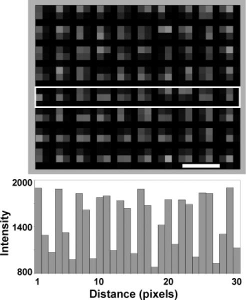
Improvement of imaging efficiency and processing. The upper panel shows a small region of a fluorescent image of an array of 1 μm superparamagnetic beads conjugated to Cy5-labeled DNA probes. A 10× objective was used, and an EMCCD with 8 × 8 μm2 pixels was properly aligned to the array so that each feature can be imaged with 3 × 3 pixels. The lower panel shows the intensity profile of the pixels in the region highlighted by the rectangle. The periodicity of the signal clearly illustrates the separation between neighboring features. The different pixel intensities reflect the slight variation in the projection of the beads relative to the pixels on the CCD sensor. The scale bar is 4.8 μm.
Rapid Magnetic Assembly of Microbead Arrays
The microbead assembly was performed within a flow cell, which consists of a 1 mm thick glass slide, a 250 μm thick silicone rubber gasket, and the cover glass with the array (Figure 1). Prior to the assembly of the flow cell, small holes were drilled through the slide and tubing connectors were fixed to the slide with epoxy. The gasket was laid onto the slide, and the middle portion was cut out to form the flow chamber. The cover glass was aligned and pressed to the gasket to form a liquid-tight seal between the slide and the cover glass.
The chamber was first rinsed with a wash buffer (WB), and then the suspension containing the DNA-conjugated microbeads was introduced into the chamber via a syringe pump. A small neodymium iron boron magnet (5848K21, McMaster-Carr) was quickly dragged along the back side of the array to pull the beads into the wells. The suspension was slightly agitated using the syringe pump, and then the beads were drawn back toward the surface of the array using the magnet. This process was repeated 3–5 times. The suspension containing any excess beads was then reclaimed, and the chamber was washed extensively with the wash buffer. The resist was dissolved by briefly exposing it to a 95% ethanol solution. The ethanol was then removed by rinsing with the wash buffer. For more sensitive biomolecules, the resist can also be removed under milder conditions using a flood exposure followed by a brief wash with a basic buffer solution.
Bright Field and Fluorescence Microscopy
Bright field images were acquired with a 63×/0.7 NA objective on a DMLFSA microscope (Leica Microsystems) equipped with an ORCA-ER CCD camera (Hamamatsu Photonics). Fluorescent images were acquired with an Axiovert 200M epifluorescence microscope (Carl Zeiss). The chamber containing the bead array was placed on a BioPrecision XY microscope stage (Ludl Electronic Products Ltd.) and illuminated with a Lambda DG-5 light source (Sutter Instrument Co.) using FITC, Cy3, and Cy5 excitation filters and a Pinkel set filter cube (Semrock). The images were acquired with either a 10×/0.45 NA or a 20×/0.80 NA objective (Carl Zeiss) and an iXon Plus 1 megapixel EMCCD camera with 8 × 8 μm2 pixels (Andor Technology). Background subtraction and image processing was performed with ImageJ.26
Atomic Force Microscopy (AFM) Imaging
The atomic force micrograph was acquired with a Multimode scanning probe microscope and NanoScope IV controller (Digital Instruments, Veeco Metrology Group). The instrument was operated in tapping mode using an AS-12NM scanner and a RTESP probe (Veeco Probes). Height and phase information was recorded using the NanoScope software, and image processing and rendering was performed using WSxM.27
Scanning Electron Microscopy (SEM) Imaging
Scanning electron micrographs were acquired with a Phillips XL30 environmental SEM in high-vacuum mode at 10 kV. All samples were washed with deionized water, air-dried, and then sputter-coated with a thin layer of gold or chromium using a Denton Discovery 18 sputter system or EMITECH K575X sputter tool prior to SEM imaging.
RESULTS AND DISCUSSION
Using this procedure, we are able to fabricate wafer-scale high-density arrays of microbeads on glass coverslips. Specifically, we have demonstrated that large arrays of wells with micrometer to submicrometer dimensions can be fabricated on derivatized cover glass and that millions of DNA-conjugated superparamagnetic beads can be assembled within these wells in seconds by active manipulation with a magnetic field gradient. Example light micrographs, AFM, and SEM images of these arrays are shown in Figures 2 and 3.
Figure 2.

High-density arrays of wells and microbeads. (A) AFM image of a small section of an array of wells in photoresist on a glass coverslip. (B) Light micrograph and (C) SEM image of a small section of an array of wells partially filled with streptavidin-conjugated superparamagnetic microbeads. We left about half of the wells unfilled for illustrative purposes. (D) Light micrograph and (E) SEM image of a highly ordered array of microbeads in wells in the photoresist. (F) SEM image of an array of microbeads after removal of the photoresist. This array was fabricated on a 50 × 75 × 0.170 mm3 glass coverslip and contained over 300 million wells. The wells are approximately 500 nm deep, 1.2 μm in diameter, and have a center-to-center spacing of 2.4 μm. The beads have an average diameter of 1.05 μm with a maximum coefficient of variation of 3% according to the manufacturer's specifications. The scale bar in the xy-plane in (A) is 2 μm. The vertical dimension in this AFM image is not to scale. The scale bars in (B) and (D) are 24 μm.
Without the use of a magnetic field gradient, we found that the wells were filled very slowly and many of them remain empty despite prolonged incubation periods. This process is even more problematic when using beads with densities near that of water. Dewetting could be used to ensure a higher filling efficiency, but it could take hours to days to fill the wells on a large array using this approach because of the slow rate at which the liquid front must move (~1 mm/h).21 The application of a magnetic field gradient overcomes this limitation by rapidly concentrating the superparamagnetic beads near the surface of the array and pulling them into the wells. Since the exposure to the magnetic field gradient is very brief and does not require micromagnets or solenoids, the formation of bead aggregates is transient and does not lead to any defects on the array.25 Real-time monitoring of the filling process can be used to determine when the assembly process is complete. Unbound beads can be drawn away from the surface using the magnet, which allows us to observe the surface of the array without having to remove the excess beads from the chamber.
The majority of the wells on a large array can be filled within seconds by quickly dragging an edge of a strong permanent magnet across the bottom of the glass substrate. By repeatedly agitating the suspension and concentrating the beads at the surface using the magnet, greater than 99.9% of the wells can be filled in less than 1 min. Achieving this level of filling in such a short period of time requires a suspension containing at least 1.5 × 10⁶ beads/μL for an array of wells with a pitch of 2.4 μm in a chamber with a height of 250 μm. This concentration corresponds to approximately twice as many beads as there are wells on this array. The use of lower concentrations will generally result in an increase in the number of empty wells and the amount of time required to fill the wells. However, even if the bead to well ratio is reduced to one, we have shown that over 95% of the wells can be filled in less than 5 min.
Our method also provides an easy way to recycle excess beads, and the process can be fully automated. These features may be much more difficult to implement when employing a dewetting17,28 or solvent evaporation20,29 approach. In addition, the immobilization of the beads onto the surface via biotin–streptavidin binding allows us to conduct various reactions and assays within the flow cell and perform rigorous washing steps without worrying about beads falling out of their wells.29 Another advantage of using a capture mechanism rather than relying only on van der Waals interactions18–21 to hold the beads in place is that it permits the removal of the resist after the assembly process is complete. This helps to remove any remaining unbound beads from the surface, reduces background fluorescent generated by the resist, and prevents the nonspecific binding of other molecules that will eventually be introduced into the flow cell as part of an assay or reaction. These important benefits can still be realized even if biotin–streptavidin chemistry is not suitable for a particular application. In such cases our process could be modified to incorporate other affinity binding modalities or covalent bonds if the surfaces of the beads and the glass substrate are appropriately functionalized, e.g., with alkyne groups on the beads and azide groups on the glass surface using the “click chemistry” strategy.30,31
In comparison to fiber-optic bead arrays,19,20,29 our approach offers more flexibility in terms of the substrates that can be used and the format and size of the arrays that can be produced. For instance, silicon wafers or various plastics could be used instead of glass. In addition, the photolithographic process allows us to easily modify every geometric parameter relevant to our arrays and gives us the ability to align the beads to virtually any CCD sensor using a standard microscope rather than a fiber-optic couple. Many of the beads in our figures are not perfectly aligned with one another because the wells are slightly larger than the beads. The use of oversized wells results in shorter bead assembly times and ensures that beads with larger than average diameters can still be captured. However, the well size can be reduced to match the bead size if an array with more precise alignment is required. We have demonstrated that well diameters can be adjusted to some degree by varying the exposure time, which gives this process greater flexibility in terms of the size of beads than can be used with a given photomask.
Not only does our fabrication process result in enhanced packing efficiency, but the usage of these ordered arrays can also improve imaging efficiency and dramatically simplify image processing. The imaging efficiency, in terms of the number of pixels needed to image each feature, is given by (Md/p)2, where M is the magnification, d is the periodic distance between two adjacent features, and p is the pixel size. A feature refers to a bead and its surrounding space, and the equation assumes that the array is properly aligned to the CCD sensor. To achieve optimal alignment, precise adjustments to both the array and CCD are usually required. Translational positioning of the array can be performed using a motorized stage, whereas angle adjustments can be made by rotating the camera. As shown in Figure 4, we have demonstrated that it is feasible to use only 3 × 3 pixels on the CCD sensor to image each feature with our current bead arrays and microscope configuration. In this image, the fluorescence from each bead is projected onto a maximum of 2 × 2 pixels and each signal cluster is separated from one another by a single row and column of pixels. At this level of efficiency, more than 105 beads can be imaged in a single field of view with our 1 megapixel camera. Profile plots across any three rows or columns in this figure reveal a clear distinction between the beads despite single-pixel separation between adjacent beads.
Further improvements to both the imaging and packing efficiencies can be achieved by using smaller beads on an array with a reduced pitch as long as the format of the array matches that of the CCD sensor. For example, 4 pixels per feature could be achieved if a 10× objective and a CCD camera with 8 × 8 μm2 pixels are used to image 0.8 μm or smaller beads assembled into 0.8 μm wells that have a center-to-center spacing of 1.6 μm. In this case each bead would fill only one pixel and be separated from each neighboring bead by a single pixel. If we use a CCD camera with a larger pixel size, e.g., 16 × 16 μm2, the maximum imaging efficiency of 1 pixel per feature could be feasible. However, special features may need to be built into the array to serve as markers for precise alignment of the array to the pixels of the CCD sensor. The maximum packing efficiency that can be achieved depends upon the optics and the wavelength of light being used for imaging. For instance, when using a diffraction-limited objective with a high numerical aperture, e.g., a 40× oil lens with 1.3 NA, and visible light with a wavelength of 500 nm, the theoretical minimum spacing of the features is approximately 230 nm. The efficient production of wafer-scale arrays with features on this scale will require deep UV photolithography or nanoimprint lithography. Our method can be modified slightly to accommodate these fabrication methods by derivatizing the glass surface after the fabrication of the wells to prevent the destruction of the biotin moieties during the imprinting or etching steps.32–34
With the densities we have shown here, more than 20 million beads can be arrayed in 1 cm2. We have also demonstrated the ability to fabricate arrays of wells with dimensions as small as 0.8 μm and densities approaching 40 million wells/cm2 over a large area on a cover glass with the stepper system we used. With the appropriate beads and arrays of wells, many copies of a human genome can be fragmented (e.g., 100–1000 bp), cloned, and assembled onto a single glass coverslip. The genomic DNA clones can be generated by amplification of single DNA molecules on beads by PCR in microemulsions.35 The use of these high-density arrays of DNA-conjugated microbeads can significantly increase the throughput and capacity of the emerging genome sequencing technologies7–9 and other array-based genomic and proteomic assays. In our arrays, there is a minimal amount of space between each bead and overlap is virtually eliminated. These characteristics will also help reduce reagent waste and the need for expensive computer clusters to perform the image analysis and base calling algorithms.
CONCLUSIONS
We have developed a scalable method for fabricating large-scale, high-density arrays of DNA-conjugated superparamagnetic microbeads on glass coverslips. The single-step photolithographic process along with the speed and simplicity of the bead assembly step gives our approach many advantages over existing bead array technologies.15–25 We have shown that arrays with densities approaching 20 million beads/cm2 can be produced over an area as large as 12 cm2 using well-established, production-scale manufacturing processes. Our low-defect arrays are free of background caused by nonspecifically bound beads and are compatible with automated processes, microfluidics devices, and conventional microscopy. The highly ordered arrays, when properly sized and aligned to a given CCD sensor, can also greatly improve imaging efficiency and reduce the complexities of image processing. We have shown that as few as 3 × 3 pixels are required to image each feature. By combining these arrays with the emerging sequencing technologies, the time and cost required to sequence a human genome could be reduced by at least 1 order of magnitude. The described method can also be used for fabricating and assembling arrays of other molecules such as antigens, lipids, and proteins.
ACKNOWLEDGMENT
We thank Dr. Brian Thibeault and Bob Hill at the Nanotech Facility at the University of California, Santa Barbara, and Ryan Anderson, Larry Grissom, and Dr. Maribel Montero at the Calit2 Nano3 Facility at the University of California, San Diego for providing advice, training, and technical support to K.D.B. Access to the UCSB Nanotech facility was made possible by the NSF National Nanotechnology Infrastructure Network. This work was supported in part by the NIH/NHGRI (HG003587 and HG004130) and by NSF under a CAREER award to X.H. (BES-0547193).
References
- (1).Fodor SPA, Read JL, Pirrung MC, Stryer L, Lu AT, Solas D. Science. 1991;251:767–773. doi: 10.1126/science.1990438. [DOI] [PubMed] [Google Scholar]
- (2).Schena M, Shalon D, Davis RW, Brown PO. Science. 1995;270:467–470. doi: 10.1126/science.270.5235.467. [DOI] [PubMed] [Google Scholar]
- (3).Lockhart DJ, Dong H, Byrne MC, Follettie MT, Gallo MV, Chee MS, Mittmann M, Wang C, Kobayashi M, Horton H, Brown EL. Nat. Biotechnol. 1996;14:1675–1680. doi: 10.1038/nbt1296-1675. [DOI] [PubMed] [Google Scholar]
- (4).Zhu H, Bilgin M, Bangham R, Hall D, Casamayor A, Bertone P, Lan N, Jansen R, Bidlingmaier S, Houfek T, Mitchell T, Miller P, Dean RA, Gerstein M, Snyder M. Science. 2001;293:2101–2105. doi: 10.1126/science.1062191. [DOI] [PubMed] [Google Scholar]
- (5).Emrich CA, Tian H, Medintz IL, Mathies RA. Anal. Chem. 2002;74:5076–5083. doi: 10.1021/ac020236g. [DOI] [PubMed] [Google Scholar]
- (6).Margulies M, Egholm M, Altman WE, Attiya S, Bader JS, Bemben LA, Berka J, Braverman MS, Chen YJ, Chen Z, Dewell SB, Du L, Fierro JM, Gomes XV, Godwin BC, He W, Helgesen S, Ho CH, Irzyk GP, Jando SC, Alenquer MLI, Jarvie TP, Jirage KB, Kim J-B, Knight JR, Lanza JR, Leamon JH, Lefkowitz SM, Lei M, Li J, Lohman KL, Lu H, Makhijani VB, McDade KE, McKenna MP, Myers EW, Nickerson E, Nobile JR, Plant R, Puc BP, Ronan MT, Roth GT, Sarkis GJ, Simons JF, Simpson JW, Srinivasan M, Tartaro KR, Tomasz A, Vogt KA, Volkmer GA, Wang SH, Wang Y, Weiner MP, Yu P, Begley RF, Rothberg JM. Nature. 2005;437:376–380. doi: 10.1038/nature03959. [DOI] [PMC free article] [PubMed] [Google Scholar]
- (7).Shendure J, Porreca GJ, Reppas NB, Lin X, McCutcheon JP, Rosenbaum AM, Wang MD, Zhang K, Mitra RD, Church GM. Science. 2005;309:1728–1732. doi: 10.1126/science.1117389. [DOI] [PubMed] [Google Scholar]
- (8).Bentley DR. Curr. Opin. Genet. Dev. 2006;16:545–552. doi: 10.1016/j.gde.2006.10.009. [DOI] [PubMed] [Google Scholar]
- (9).Church GM. Sci. Am. 2006;294:46–54. doi: 10.1038/scientificamerican0106-46. [DOI] [PubMed] [Google Scholar]
- (10).Johnson DS, Mortazavi A, Myers RM, Wold B. Science. 2007;316:1497–1502. doi: 10.1126/science.1141319. [DOI] [PubMed] [Google Scholar]
- (11).Thibault C, Berre VL, Casimirius S, Trévisiol E, François J, Vieu C. J. Nanobiotechnol. 2005;3:1–12. doi: 10.1186/1477-3155-3-7. [DOI] [PMC free article] [PubMed] [Google Scholar]
- (12).Pla-Roca M, Fernandez JG, Mills CA, Martinez E, Samitier J. Langmuir. 2007;23:8614–8618. doi: 10.1021/la700572r. [DOI] [PubMed] [Google Scholar]
- (13).Tan H, Huang S, Yang KL. Langmuir. 2007;23:8607–8613. doi: 10.1021/la701258c. [DOI] [PubMed] [Google Scholar]
- (14).Nam J-M, Han SW, Lee K-B, Liu X, Rathner MA, Mirkin CA. Angew. Chem., Int. Ed. 2004;43:1246–1249. doi: 10.1002/anie.200353203. [DOI] [PubMed] [Google Scholar]
- (15).Xia Y, Yin Y, Lu Y, McLellan J. Adv. Funct. Mater. 2003;13:907–918. [Google Scholar]
- (16).Michel R, Reviakine I, Sutherland D, Fokas C, Csucs G, Danuser G, Spencer ND, Textor M. Langmuir. 2002;18:8580–8586. [Google Scholar]
- (17).Cui Y, Bjork MT, Liddle JA, Sonnichsen C, Boussert B, Alivisatos AP. Nano Lett. 2004;4:1093–1098. [Google Scholar]
- (18).Steemers FJ, Gunderson KL. Biotechnol. J. 2007;2:41–49. doi: 10.1002/biot.200600213. [DOI] [PubMed] [Google Scholar]
- (19).Michael KL, Taylor LC, Schultz SL, Walt DR. Anal. Chem. 1998;70:1242–1248. doi: 10.1021/ac971343r. [DOI] [PubMed] [Google Scholar]
- (20).Ferguson JA, Steemers FJ, Walt DR. Anal. Chem. 2000;72:5618–5624. doi: 10.1021/ac0008284. [DOI] [PubMed] [Google Scholar]
- (21).Yin Y, Lu Y, Gates B, Xia Y. J. Am. Chem. Soc. 2001;123:8718–8729. doi: 10.1021/ja011048v. [DOI] [PubMed] [Google Scholar]
- (22).Li AX, Seul M, Cicciarelli J, Yang JC, Iwaki Y. Tissue Antigens. 2004;63:518–528. doi: 10.1111/j.0001-2815.2004.00219.x. [DOI] [PubMed] [Google Scholar]
- (23).Wen W, Wang N, Zheng DW, Chen C, Tu KN. J. Mater. Res. 1999;14:1186–1189. [Google Scholar]
- (24).Roberts LA, Crawford AM, Zappe S, Jain M, White RL. IEEE Trans. Magn. 2004;40:3006–3008. [Google Scholar]
- (25).Yellen BB, Friedman G. Langmuir. 2004;20:2553–2559. doi: 10.1021/la0352016. [DOI] [PubMed] [Google Scholar]
- (26).Abramoff MD, Magelhaes PJ, Ram SJ. Biophotonics Int. 2004;11:36–42. [Google Scholar]
- (27).Horcas I, Fernandez R, Gomez-Rodriguez JM, Colchero J, Gomez-Herrero J, Baro AM. Rev. Sci. Instrum. 2007;78:013705. doi: 10.1063/1.2432410. [DOI] [PubMed] [Google Scholar]
- (28).Yin Y, Lu Y, Xia Y. J. Am. Chem. Soc. 2001;123:771–772. doi: 10.1021/ja0031873. [DOI] [PubMed] [Google Scholar]
- (29).Gunderson KL, Kruglyak S, Graige MS, Garcia F, Kermani BG, Zhao C, Che D, Dickinson T, Wickham E, Bierle J, Doucet D, Milewski M, Yang R, Siegmund C, Haas J, Zhou L, Oliphant A, Fan J-B, Barnard S, Chee MS. Genome Res. 2004;14:870–877. doi: 10.1101/gr.2255804. [DOI] [PMC free article] [PubMed] [Google Scholar]
- (30).Wu P, Feldman AK, Nugent AK, Hawker CJ, Scheel A, Voit B, Pyun J, Frechet JM, Sharpless KB, Fokin VV. Angew. Chem., Int. Ed. 2004;43:3928–3932. doi: 10.1002/anie.200454078. [DOI] [PubMed] [Google Scholar]
- (31).Rozkiewicz DI, Gierlich J, Burley GA, Gutsmiedl K, Carell T, Ravoo BJ, Reinhoudt DN. ChemBioChem. 2007;8:1997–2002. doi: 10.1002/cbic.200700402. [DOI] [PubMed] [Google Scholar]
- (32).Hoff JD, Cheng L-J, Meyhofer E, Guo LJ, Hunt AJ. Nano Lett. 2004;4:853–857. [Google Scholar]
- (33).Gao H, Tan H, Zhang W, Morton K, Chou SY. Nano Lett. 2006;6:2438–2441. doi: 10.1021/nl0615118. [DOI] [PubMed] [Google Scholar]
- (34).Truskett VN, Watts MPC. Trends Biotechnol. 2006;24:312–317. doi: 10.1016/j.tibtech.2006.05.005. [DOI] [PubMed] [Google Scholar]
- (35).Dressman D, Yan H, Traverso G, Kinzler KW, Vogelstein B. Proc. Natl. Acad. Sci. U.S.A. 2003;100:8817–8822. doi: 10.1073/pnas.1133470100. [DOI] [PMC free article] [PubMed] [Google Scholar]