Abstract
High-moment synthetic antiferromagnetic (SAF) nanoparticles were produced using 4 in. diameter stamps made by self-assembly and nanosphere lithography of latex nanospheres. This leads to a significant increase in particle yield over a pre-existing technique which utilizes a 1 cm2 stamp patterned using e-beam lithography. Changes in nanopillar dimensions from the self-assembled stamps and variations in the associated processing conditions can lead to the fabrication of particles with different dimensions. We demonstrate that it is possible to produce reasonably uniformly sized SAFs with diameters from 70 nm upward using self-assembled stamps. The particles exhibit low remanence at low externally applied magnetic fields, and that the saturation magnetization more than double that for conventional iron oxide nanoparticles.
INTRODUCTION
Magnetic nanoparticles (MNPs) are promising candidates for biomedical applications such as cell sorting and magnetic separation,1, 2, 3 where target biological analytes are labeled with MNPs and then separated from the unwanted entities using a fluid-based magnetic separation technique.4, 5 For this application, the MNPs should be uniform in shape, size, and composition and exhibit high magnetic moment for low external applied field and low magnetic moment at zero field. It would also be desirable if “multiplexing” can be achieved by using MNPs with distinctive magnetic responses to target multiple entities within a single analyte.
Typical MNPs are iron oxides (e.g., magnetite) and are synthesized using chemical means. For these nanoparticles to possess low remanence at zero applied magnetic field, their sizes need to be constrained to less than 20 nm as they become ferromagnetic at larger diameters.6 Because of the small magnetic volume per nanoparticle, the resulting magnetic moment tends to be low. To overcome this issue, synthetic antiferromagnetic (SAF) nanoparticles7, 8, 9 were developed. SAFs are fabricated using nanoimprint lithography, direct deposition of multilayer films, and retrieval in liquid phase via a release process. Such physical fabrication techniques enable accurate control of particle shape, size, and composition. Each SAF is composed of two Co90Fe10 layers separated by a nonmagnetic Ru spacer layer, so the two ferromagnetic layers to interact primarily through magnetostatic interactions, with like poles repelling. Ta is used as a protective capping layer to passivate and stabilize the suspended nanoparticles.
For the SAFs to realize their full potential, large volumes of particles are required. A current obstacle in increasing nanoparticle production is the size of the stamp. Using e-beam lithography, we previously used 1 cm2 area with 100 nm pillars at 300 nm pitch, allowing 109 particles to be fabricated per imprint. In this paper, we demonstrate that it is possible to increase the nanoparticle yield per imprint and fabricate uniformly sized particles using large self-assembled stamps made by spin coating latex nanospheres10, 11, 12, 13 on 4 in. diameter Si wafers. By varying an oxygen plasma etching time and the undercut development time, the diameter of the imprinted holes can be varied.
EXPERIMENTS
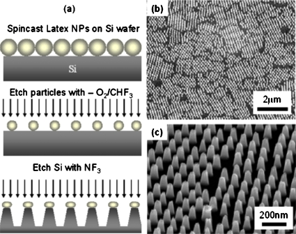
The SAFs described in this study were produced from stamps made by latex nanospheres which had been self-assembled on 4 in. diameter Si substrates [Fig. 1a]. Carboxylate-modified latex nanospheres with diameter of 100 or 200 nm (Duke Scientific) were first spin coated onto the Si substrates. The coated substrates then reactive ion etched (with O2∕CHF3 gas mixture) to produce a nanosphere mask. The Si was then etched to form nanopillars and the nanosphere residue was dissolved in toluene. The etched wafer then consists of a sub-100 nm nanopillars and is used for nanoimprinting fabrication of SAF. Scanning electron microscopy (SEM) characterization reveals that the self-assembled stamp [Fig. 1b] possesses large, partially ordered, area arrays of nanopillars. Figure 1c shows the nanopillars on a typical self-assembled stamp after the latex spheres had been dissolved. This use of large self-assembled stamps leads to a 100-fold increase in the number of SAFs produced per imprint.7
Figure 1.
(a) Schematic illustration of the fabrication of self-assembled stamps using nanosphere lithography. (b) SEM image of a self-assembled stamp showing that it contains large area arrays of nanopillars matching the initial spin cast latex nanospheres. (c) SEM image showing the nanopillars on a typical self-assembled stamp after the latex spheres had been dissolved.
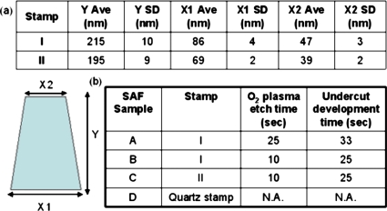
Details of the physical fabrication process of SAF nanoparticles have been described in literature.7, 9 In this study, particles with structure Ta2∕Ru2∕Co90Fe106∕Ru3∕Co90Fe106∕Ru2∕Ta10 (numbers denote nominal film thicknesses in nm) were deposited on templated holes produced by two self-assembled stamps whose dimensions are given in Table 1(a). Then, the substrate-bound SAFs were ion milled, released, and suspended in water.7, 9 As a control, particles fabricated using an e-beam patterned master stamp (Obducat) were also analyzed. Four samples were investigated. Table 1(b) lists the type of stamp and processing conditions. Samples A and B used the same self-assembled stamp but the different oxygen etch times, of 25 and 10 s, respectively, resulted, in different hole sizes.
Table 1.
(a) Dimensions of the two self-assembled stamps that were used in this study. (b) List of particles, stamps from which they were fabricated and their associated processing conditions.
 |
Transmission electron microscopy (TEM) was used to characterize the morphology and size distribution of the nanoparticles. Samples were drop cast on 3 mm diameter TEM Cu grids coated with an ultrathin layer of carbon. TEM analyses were performed using a Philips CM20 FEG-TEM operated at 200 kV. Magnetic hysteresis loops of substrate bound and released nanoparticles were measured using alternating gradient magnetometry (AGM) (Micromag 2900, Princeton Measurements Corp., Princeton, NJ).
RESULTS AND DISCUSSION
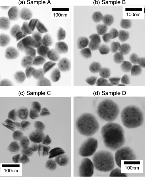
Figures 2a, 2b, 2c, 2d are representative TEM bright field images of samples A–D analyzed in this study. The control (sample D) comprising SAFs fabricated on the master stamp has the largest diameter particles and demonstrates superior uniformity in diameter. Of the three samples that had utilized self-assembled stamps, the particles in A have the largest dimensions. This is consistent with the longer oxygen plasma etch time and a longer undercut development time resulting in the formation of larger holes from the initial imprint. Sample C is the least uniform with a mixture of dome and conically shaped particles.
Figure 2.
Representative TEM BF images of the four SAF samples analyzed in the present study. Samples A–C are constructed out of self-assembled stamps. Sample D consists of particles fabricated from the master stamp patterned by e-beam lithography.
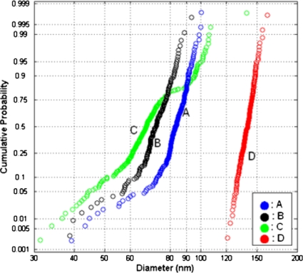
We measured the diameters (defined as the base for particles that have landed on their sides) of >200 particles from each sample to characterize their size distribution. Plots of cumulative probability distributions against particle size on a log-log scale are seen in scale in Fig. 3. Particles whose data points are found to approximate a straight line on such plots can be described by a lognormal size distribution model, which is characteristic of chemically synthesized particles.14, 15 The particle statistics are given in Table 2. The plot representing SAF nanoparticles fabricated with the quartz stamp (sample D) consists of a straight line with a steep gradient, showing that these particles are highly uniform in size with <5% standard deviation (Table 2). Of the four samples investigated, particles from C have the smallest dimensions since stamp II consisted of smaller nanopillars. Particles fabricated using these self-assembled stamps are not described by a lognormal distribution (i.e., the log-log variation on the cumulative plot is not linear). This may be because their final dimensions are determined by process steps, such as oxygen plasma etching, undercut development time, and ion milling, which differ vastly from the nucleation-and-growth processes the lognormal size distribution model for chemically synthesized nanoparticles.14, 16
Figure 3.
Particle size distribution plots of the four SAF nanoparticle samples analyzed in the present study, showing the remarkable uniformity of the SAFs fabricated using the master stamp, although with significantly larger dimensions.
Table 2.
SAF nanoparticle size distribution statistics.
| Sample | Mean diameter (nm) | Median diameter (nm) | Standard deviation (nm) | Standard deviation (%) |
|---|---|---|---|---|
| A | 83 | 83 | 9 | 11 |
| B | 72 | 72 | 9 | 12 |
| C | 70 | 67 | 16 | 23 |
| D | 139 | 140 | 7 | 5 |
Figure 4 shows the magnetic hysteresis loops of sample A before and after ion milling, and after the particles were released in water. The shapes of these M-H loops are representative of B and C as well. The SAFs exhibit a high saturation magnetization of ∼840 emu∕cm3, which is more than twice that of superparamagnetic iron oxide nanoparticles (∼300–400 emu∕cm3).17 Table 3 shows the ratio of the magnetic remanence (Mr) to magnetic saturation (Ms) of the four samples before and after the ion milling process, and after suspension in water. All samples show an increase in Mr after ion milling, which may be attributed to damage during the process. Moreover, this process creates dome-shaped SAF particles that may cause a mismatch in magnetic moment between the two ferromagnetic layers.
Figure 4.
Magnetic hysteresis loops of sample A before and after ion milling, and after the particles had been released in water. There is a reduction in the saturation field and an increase in the openness of the magnetic hysteresis loop in high field regions for the latter.
Table 3.
Mr∕Ms ratios of the four samples before ion mill, after ion mill and after release in water.
| Sample | Mr∕Ms | ||
|---|---|---|---|
| Before ion mill | After ion mill | After release | |
| A | 0.02 | 0.12 | 0.03 |
| B | 0.04 | 0.08 | 0.03 |
| C | 0.07 | 0.10 | 0.04 |
| D | 0.02 | 0.04 | 0.03 |
There are significant changes in the M-H loops after the particles are released in water. First, there is an apparent reduction in the saturation field, which is thought to be caused by magnetic field induced chaining in solution, i.e., the fields produced by dipoles in a chain are oriented in the same direction as the applied field, thus reducing saturation fields.7, 18 There is also an increase in energy loss, as seen in the “openness” of the magnetic hysteresis loop in high field regions. The hysteresis losses may be related to magnetic interactions between particles and their rotation∕motion in solution.18
CONCLUSIONS
In summary, SAF nanoparticles can be fabricated on a large scale using self-assembled stamps. There was a hundred-fold increase in the number of nanoparticles produced per imprint using self-assembled stamps. The dimensions of the SAF nanoparticles can be varied by changing the nanopillar dimensions and by varying the oxygen plasma etch depth and undercut development time. TEM analyses show that it is possible to produce uniformly sized (<15% variation in diameter) SAFs with diameters above 70 nm using self-assembled stamps. AGM analyses show that the particles exhibit low remanence and that the saturation magnetization is more than double that for conventional iron oxide nanoparticles.
ACKNOWLEDGMENTS
This work was supported by the Stanford Center for Cancer Nanotechnology Excellence Focused on Therapy Response (CCNE-TR) grant (NIH U54), the Nanyang Technological University (Singapore) Overseas Scholarship (A.L.K.), and a Stanford Graduate Fellowship (W.H.).
References
- Berry C. C., Wells S., Charles S., and Curtis A. S. G., Biomaterials 24, 4551 (2003). 10.1016/S0142-9612(03)00237-0 [DOI] [PubMed] [Google Scholar]
- Berry C. C., J. Mater. Chem. 15, 543 (2005). 10.1039/b409715g [DOI] [Google Scholar]
- Kim D. K., Zhang Y., Voit W., Rao K. V., Kehr J., Bjelke B., and Muhammed M., Scr. Mater. 44, 1713 (2001). 10.1016/S1359-6462(01)00870-3 [DOI] [Google Scholar]
- Pankhurst Q. A., Connolly J., Jones S. K., and Dobson J., J. Phys. D: Appl. Phys. 36, R167 (2003). 10.1088/0022-3727/36/13/201 [DOI] [Google Scholar]
- Scientific and Clinical Applications of Magnetic Carriers, edited by Häfeli U., Schütt W., Teller J., and Zborowski M. (Plenum, New York, 1996). [DOI] [PMC free article] [PubMed] [Google Scholar]
- Cullity B. D., Introduction to Magnetic Materials (Addison-Wesley, Reading, MA, 1972). [Google Scholar]
- Hu W., Wilson R. J., Koh A. L., Fu A., Faranesh A. Z., Earhart C. M., Osterfeld S. J., Han S. J., Guccione S., Sinclair R., and Wang S. X., Adv. Mater. (Weinheim, Ger.) 20, 1479 (2008). 10.1002/adma.200703077 [DOI] [Google Scholar]
- Koh A. L., Hu W., Wilson R. J., Wang S. X., and Sinclair R., Ultramicroscopy 108, 1490 (2008). 10.1016/j.ultramic.2008.03.012 [DOI] [PMC free article] [PubMed] [Google Scholar]
- Koh A. L., Hu W., Wilson R. J., Wang S. X., and Sinclair R., Philos. Mag. 88, 4225 (2008). 10.1080/14786430802585133 [DOI] [Google Scholar]
- Earhart C., Hu W., Wilson R. J., and Wang S. X., Digests of the Fifth International Conference on Nanoimprint and Nanoprint Technology, 2006. (unpublished).
- Hulteen J. C. and Van Duyne R. P., J. Vac. Sci. Technol. A 13, 1553 (1995). 10.1116/1.579726 [DOI] [Google Scholar]
- Rybczynski J., Ebels U., and Giersig M., Colloids Surf., A 219, 1 (2003). 10.1016/S0927-7757(03)00011-6 [DOI] [Google Scholar]
- Haginoya C., Ishibashi M., and Koike K., Appl. Phys. Lett. 71, 2934 (1997). 10.1063/1.120220 [DOI] [Google Scholar]
- Limpert E., Stahel W. A., and Abbt M., BioScience 51, 341 (2001). 10.1641/0006-3568(2001)051[0341:LNDATS]2.0.CO;2 [DOI] [Google Scholar]
- Koh A. L. and Sinclair R., Technical Proceedings of the 2007 Nanotechnology Conference and Trade Show 4, 2007. (unpublished), p. 101.
- Shimizu I., Philos. Mag. A 79, 1217 (1999). [Google Scholar]
- Xu C. and Sun S., Polym. Int. 56, 821 (2007). 10.1002/pi.2251 [DOI] [Google Scholar]
- Wilson R. J., Hu W., Wong C. P. F., Koh A. L., Gaster R., Earhart C. M., Fu A., Heilshorn S. C., Sinclair R., and Wang S. X., J. Magn. Magn. Mater. 321, 1452 (2009). 10.1016/j.jmmm.2009.02.066 [DOI] [PMC free article] [PubMed] [Google Scholar]


