Abstract
Optoelectronic tweezers (OET) is a promising approach for the parallel manipulation of single cells for a variety of biological applications. By combining the manipulation capabilities of OET with other relevant biological techniques (such as cell lysis and electroporation), one can realize a true parallel, single-cell diagnostic and stimulation tool. Here, we demonstrate the utility of the OET device by integrating it onto single-chip systems capable of performing in-situ, electrode-based electroporation/lysis, individual cell, light-induced lysis, and light-induced electroporation.
Index Terms: Dielectrophoresis, electroporation, lysis, optical manipulation, optoelectronic tweezers
I. INTRODUCTION
Much of the difficulty in the individual manipulation of microscopic and nanoscopic objects stems from the fact that macroscale objects are used to interface with objects of many orders of magnitude (103 – 106) smaller in scale. As a result, much work has been performed to reduce the size disparity between the manipulation tool and object of interest. These techniques include, amongst others, the use of ultra-small probes (e.g., atomic force microscopy tips [1]); fixed electrode-based dielectrophoresis [2], [3]; and various microfluidic/flow-based techniques [4]. These techniques do not, however, afford the highly selective and dynamic capabilities of optical manipulation platforms. In general, optical manipulation platforms afford the user the ability to create on-demand particle traps in regions only defined by the optical pattern. Therefore, simply by translating the optical pattern, the particle of interest will follow. These virtual electrodes replace the need for physical ones (as in [2] and [3]) and, thus, greatly simplify fabrication and operation as well as lower device cost as complicated address circuitry is no longer necessary. In a sense, these techniques replace cumbersome, material-based microscale and nanoscale “tweezers” with photonic ones.
The most conventional method of optical manipulation is optical tweezers [5]. Here, a highly focused laser beam creates a large gradient in an optical field, resulting in stable particle trapping at the beam focus. Since the trapping occurs only at the focal point, true 3-D trapping can occur. Particles in scale from cells (µms) to individual molecules (nms) are routinely studied with this technique [6], [7]. However, due to the large amounts of optical power necessary to create traps of adequate stiffness, large optical intensities are necessary (~ 106 W/cm2 [8]). This makes it difficult to create and control multiple traps on the same device since multiple high-powered lasers and/or holography techniques must be employed [9]. In addition, the high optical powers can be harmful to sensitive objects, such as biological cells [10], [11].
Another form of optical manipulation that has been recently employed is that of plasmonic tweezers [12], [13]. Here, a substrate that consists of an array of nanoscopic objects (e.g., nanoparticles or lithographically defined nanoscale pillars) is illuminated with a laser beam. The small particles on the surface absorb the incident radiation into resonant plasmonic modes. Due to the tight spacing of the nanoparticles on the surface, the plasmonic modes of the particles are coupled to one another, resulting in very large and localized electric fields. The localization of these fields establishes large electric-field gradients, which cause particles in the general area to polarize and experience a dielectrophoretic force. Thus, wherever the laser illuminates the device, the electric-field gradients are produced and particle traps are created. While this technique uses lower optical intensity than optical tweezers (~ 104 W/cm2 [13]), the required intensity is still significant, requiring high-power lasers and making parallelization difficult. In addition, the conversion of plasmonic energy into heat is also an area of concern with this device, especially for biological applications. This plasmonic heating effect is exploited in other applications, such as the intracellular delivery of RNA interference plasmids [14]. Finally, due to the highly textured plasmonic substrate, observation of particle movement using dark-field microscopy is difficult.
The final method of optical manipulation, optoelectronic tweezers (OET), removes the restriction of high optical intensities imposed by the other techniques [15]. By using a photosensitive substrate and an externally applied electrical bias, incident light creates localized regions of high conductivity (in the photosensitive substrate) resulting in the creation of large electric-field gradients. Therefore, particles in the illuminated region will experience a dielectrophoretic force. Due to the conversion of optical field to electrical field, very low (< 1 W/cm2) optical powers are necessary to apply the same level of forces as optical tweezers (tens to 100 s of pN) to the particles of interest. This means that a standard data projector, or spatial light modulator (SLM), can be used for manipulation. Thousands of simultaneous traps can be created on demand for the massively parallel manipulation of single particles. Another benefit of low optical intensity is that sensitive objects, such as cells, are not adversely affected by the incident light energy making OET an ideal platform for biological applications [16]. In addition, it should be noted that the conductivity of the liquid layer plays an important role in device operation. The conductivity of the liquid must fall between the light and dark conductivity of the photosensitive layer. For example, if the liquid conductivity is too high, an insufficiently small field will be switched to the liquid when illuminated and DEP actuation cannot occur. For the devices presented here, this typically limits the liquid conductivity to <100 mS/m. For applications requiring operation in a highly conductive environment (e.g., cell culture media), we have developed a different structure utilizing phototransistors instead of photoconductors to effectively switch the field to the highly conductive liquid [17].
In addition, OET is easily integrated with other technologies to perform single-cell movement, observation, and stimulation. Here, we demonstrate three separate devices integrated with OET to: electroporate/lyse cells using a conventional microelectrode approach, selectively lyse cells using a device known as lateral-field optoelectronic tweezers (LOET) [18], and electroporate cells by using a recently reported light-induced technique. Each case study illustrates the ability to combine OET with a relevant scientific biological application.
II. OPTOELECTRONIC TWEEZERS MODALITIES
The physical mechanism of OET involves the creation of localized electric-field gradients on demand with low-intensity optical energy. The geometry and method of formation of these fields depends on device layout. Here, we will describe two different OET devices (used in the following experimental section). The first, vertical-field optoelectronic tweezers (OET), orients the field perpendicular to the device surface. The second, lateral-field optoelectronic tweezers (LOET), aligns the field parallel to the device surface. The use of either one depends on the application and requirements of the user.
A. Vertical-Field Optoelectronic Tweezers (OET)
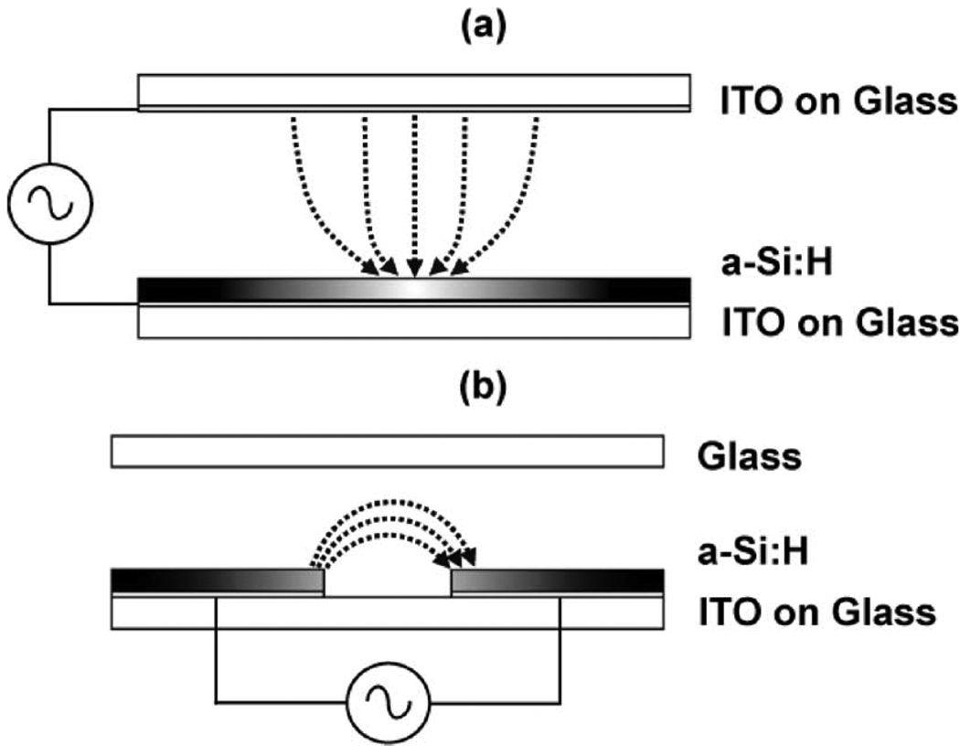
The layout of the OET device is depicted in Fig. 1(a). The top and bottom substrates consist of a commercially available glass substrate coated with a 300-nm layer of sputtered indium tin oxide (ITO) (thin-film devices). The bottom substrate is coated with a featureless 1-µm layer of hydrogenated amorphous silicon (a-Si:H) deposited via plasma-enhanced chemical vapor deposition (PECVD) (100 sccm 10%SiH4:Ar, 400 sccm Ar, 900 mTorr, 350 °C, 200 W).
Fig. 1. OET modalities.
Illumination is focused at the middle of each device. Shaded areas correspond to varying conductivity of a-Si:H due to an incident optical beam. (a) Vertical-field optoelectronic tweezers (OET). Field is oriented perpendicular to the device substrate. (b) Lateral-field optoelectronic tweezers (LOET). Field is oriented parallel (lateral) to the device substrate. (a) OET. (b) LOET.
A solution containing the particles of interest is then placed between the top and bottom substrates, which are separated by a 100-µm layer of double-sided tape. An electrical bias is then applied between ITO layers on the top and bottom substrates. Note that the applied field is perpendicular to the device substrate (i.e., vertical).
In the absence of light, most of the electric field exists in the highly resistive a-Si:H layer. Upon illumination, the incident light energy is absorbed by the a-Si:H, resulting in the creation of electron-hole pairs. This increases the conductivity of the a-Si:H by many orders of magnitude (100–1000 ×) and switches the electric field from the a-Si:H to the liquid layer in the illuminated areas [Fig. 1(a)]. Due to the localization of the light pattern, the resulting electric fields in the liquid are also localized, resulting in the formation of large electric-field gradients. Thus, the particles near the illuminated area are subjected to these field gradients and feel a dielectrophoretic force.
B. Lateral-Field Optoelectronic Tweezers (LOET)
In LOET, the field is oriented parallel to the device substrate (i.e., laterally). This is accomplished by patterning a set of interdigitated electrodes consisting of a stack of ITO and a-Si:H [Fig. 1(b)]. The device fabrication is identical to the normal OET device described previously. However, there is an additional processing step following the PECVD a-Si:H deposition during which the interdigitated electrodes are defined. This is accomplished by first patterning and etching the a-Si:H in a plasma etcher (66 sccm 90% SF6/10%O2, 100 W, 80 mTorr) and subsequent wet etching of the ITO (38% HCl).
A solution containing the particles to be actuated is then sandwiched between the LOET substrate and an arbitrary top substrate separated by a 100-µm layer of double-sided tape. It is important to note that the LOET device does not require an electrically conductive top substrate such as the normal OET device. Electrical bias is applied across the two interdigitated electrodes. In the absence of light, most of the electric field exists in the a-Si:H and not in the liquid layer. However, when illuminated, the conductivity of the a-Si:H increases dramatically and results in the field being switched from the a-Si:H to the liquid volume between the electrodes in the illuminated region [Fig. 1(b)]. As before, particles near the illuminated region respond to the light-induced electric-field gradients via dielectrophoresis.
One of the major benefits of the LOET is the fact that a conductive top substrate (which is required for the original OET device) is no longer necessary. This allows straightforward integration of the LOET device with microfluidic channels. However, if the size of the particle is too small relative to the width and spacing of the electrode fingers, movement is restricted to only one lateral dimension (as opposed to the traditional OET device where movement is in both lateral dimensions). This is because if the electrode or gap between adjacent electrodes is too wide compared to the particle, the field gradients induced in adjacent gaps will be too weak to affect the particle. Therefore, one must take into consideration the particle size when designing the LOET device.
III. EXPERIMENTAL PROTOCOL
A. Experimental Setup
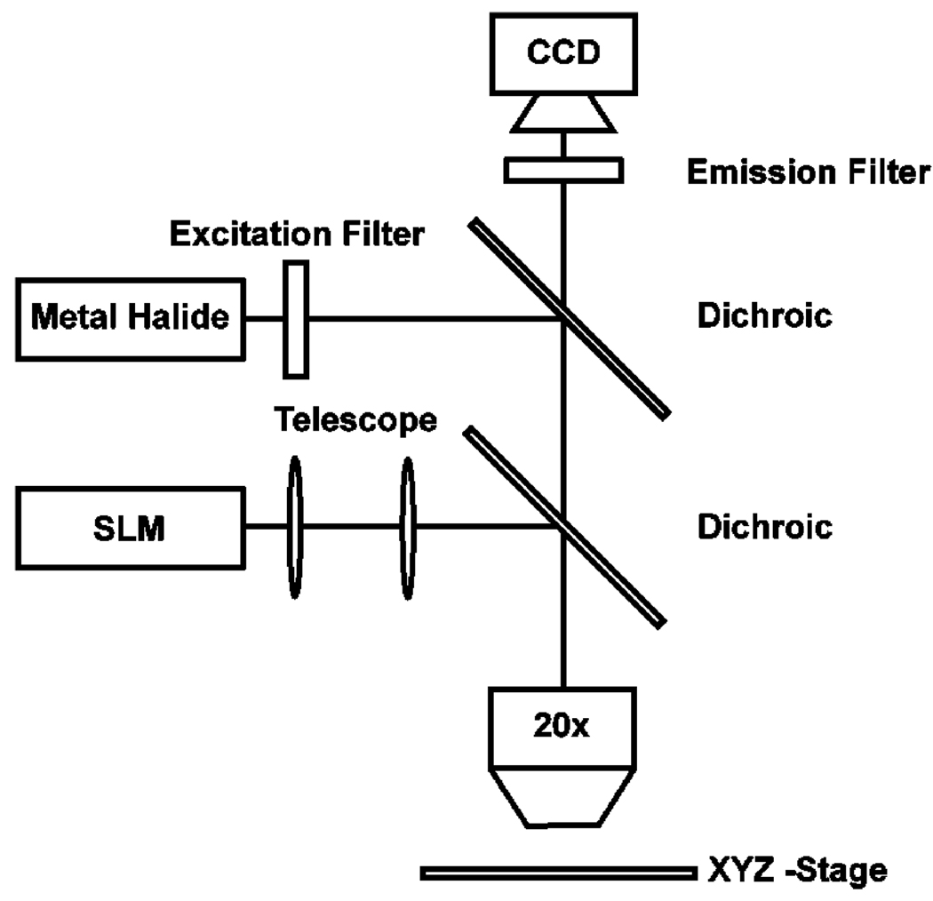
The experimental setup is depicted in Fig. 2. The custom-built setup consists of a 20 × objective mounted above the sample. The optical patterns used for manipulation and electroporation are generated on a PC and focused on the substrate via a commercially available spatial light modulator/projector (SLM) (Dell 2400MP) and dichroic filter. Bright field and fluorescence illumination is provided via a metal halide lamp (EXFO, XCite 120) coupled with a series of filters/dichroics specific to the fluorophore under investigation (Chroma Technology). Viewing occurs through a topside CCD camera (Sony, XCD-X710CR). Finally, electrical bias (0–10 kV/cm, 100 kHz) is provided with a standard function generator (Agilent 33220A).
Fig. 2. Experimental Setup.
A standard data projector/SLM is used to generate optical patterns on the device surface. A metal halide lamp provides bright field illumination and, when coupled with appropriate filters, fluorescent imaging of the device. Viewing occurs through a topside CCD camera.
B. Cell Preparation
HeLa cells at a concentration of 2 × 10⁶ cells/ml were washed three times and suspended in a commercially available electroporation buffer (Cytopulse Sciences, Cytoporation Media T, 10 mS/m). Propidium iodide (PI) dye (Invitrogen) was then added to the solution at a concentration of 2 µM to monitor cell lysing and electroporation. PI is a membrane-impermeable dye which has low auto fluorescence. However, in the presence of DNA, the dye will bind to the nucleic acids and, as a result, strongly fluoresce red. Therefore, PI is an accurate indicator of cellular membrane perforation.
IV. APPLICATIONS OF OET FOR CELL MANIPULATION AND STIMULATION
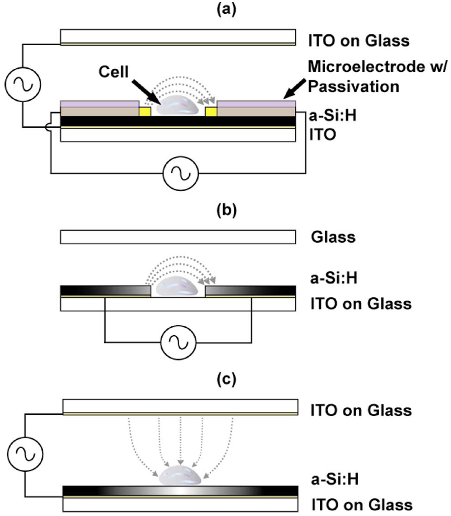
Two techniques that are of interest for integration onto lab-on-a-chip technologies are electroporation and lysis. Here, we demonstrate three device geometries, integrated with OET, to effect parallel, single-cell electroporation, and/or lysis. The three geometries are shown in Fig. 3 and are discussed in detail.
Fig. 3. Applications of OET for cell manipulation and simulation.
The shaded areas correspond to varying conductivity of a-Si:H due to incident optical beam [(b) and (c) only]. (a) OET integrated with on-chip microelectrodes for single-cell electroporation/lysis. (b) LOET used to affect single-cell, light-induced cell lysis. (c) OET used to affect single-cell, light-induced electroporation. (a) Microelectrode-based electroporation/lysis with OET. (b) LOET for parallel single-cell lysis. (c) Electrodeless light-induced electroporation with QET.
Electroporation is a common technique for the introduction of exogenous molecules across the otherwise impermeable cell membrane. It is commonly used for applications ranging from genetic transfection to the study of cell-to-cell signaling. Temporary permeation of the cellular membrane is achieved in electroporation by subjecting the cell to an external electric field. If the field strength is large enough, it causes a temporary depolarization of the cell’s bi-lipid membrane. This results in the formation of pores, which allow molecules in the extra-cellular space to pass across the otherwise impermeable membrane. The size of these pores is greatly dependant on field strength. If the field is too strong, the pores will not reseal, resulting in cell death and/or cell lysis. However, if the field is properly controlled, the pores can reseal resulting in reversible electroporation. Conventional commercial techniques, such as cell lysis, are limited by either low throughput or low selectivity. Much work has been done to create microscale poration chips to alleviate these issues. Techniques for microporation platforms typically include microelectrode [19], physical field constriction [20], optoporation [21], chemical [22], and microinjection [23].
Controlled cell lysis is routinely used for the extraction of intracellular contents, such as DNA and proteins. There are a multitude of techniques used for lysis including chemical [24], mechanical [25], thermal [26], optical [27], and electrical [28]. These techniques are limited by either low throughput (optical) or limited selectivity (chemical, thermal, electrical, mechanical). The electrical method of cell lysis is simply electroporation at very high fields so that the induced pores do not reseal and intracellular contents are released into the surrounding medium.
A. Microelectrode-Based Electroporation/Lysis With OET
Electroporation/lysis with microelectrodes is one of the simplest techniques wherein individually addressable microelectrodes are patterned onto the device substrate and subject cells to controlled electric-field doses. Since selectivity will scale with electrode number, the complexity and cost of the device increases substantially if one wants to achieve true single-cell accuracy (i.e., a large number of electrodes will require multiple metal layers with a need for on-chip addressing and decoding). A more ideal approach would be to have a small number of electrodes that form electroporation sites for individual cells and then use a technique such as OET to bring the cells of interest to the electroporation sites. By combining OET’s ability to select and manipulate individual cells with microelectrodes, high selectivity can be achieved with far fewer electrodes [Fig. 3(a)].
A simple two-mask process was used to integrate the microelectrodes onto the traditional vertical-field OET. The OET device was fabricated as described previously. The electrodes were defined via a liftoff process using a 10-nm/60-nm layer of evaporated Cr/Au. Isolation of the electrodes was then achieved by patterning another layer of photoresist on top of the electrode leads.
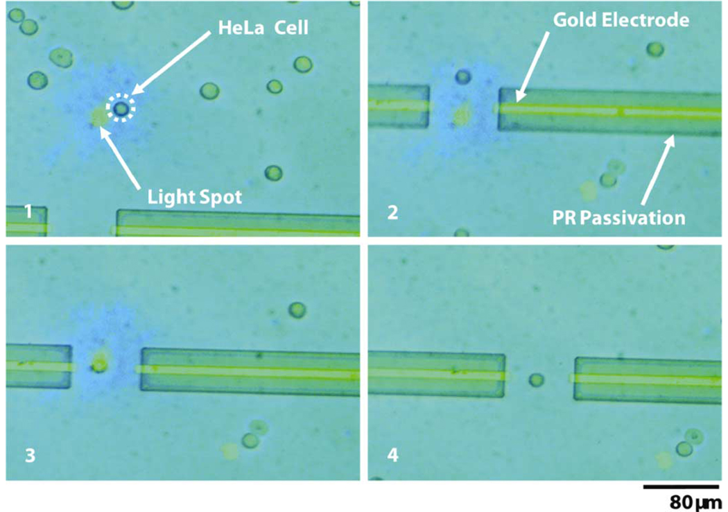
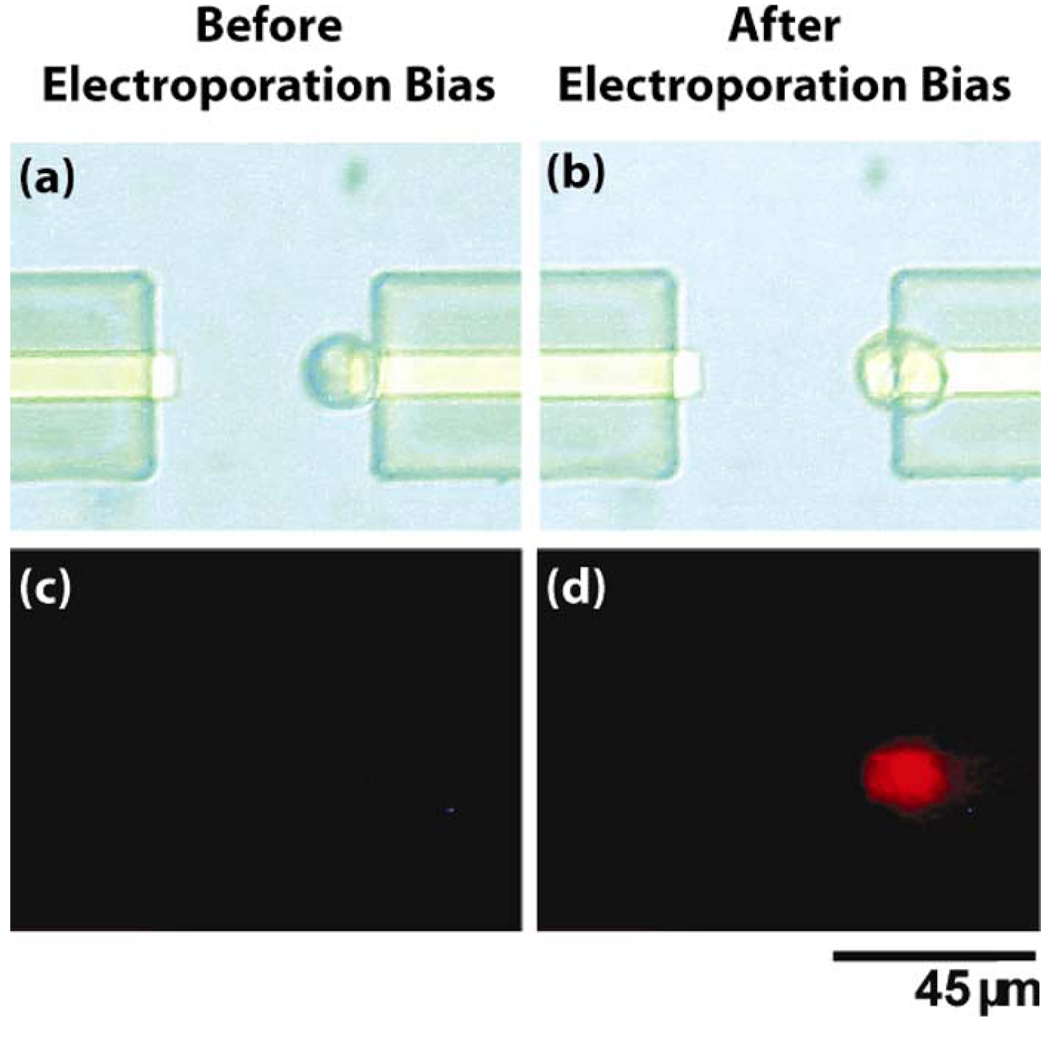
In order to demonstrate the capabilities of integrating OET with the microelectrodes for single-cell electroporation/lysis, we place a population of suspended cells onto the integrated device. We then select a single cell with OET and move it from the general population to the region between the two electrodes (5 Vppk, 100 kHz). This process can be seen in Fig. 4. One can see that in panel 4, the cell is located directly between the two Au electrodes and is awaiting the electroporation bias.
Fig. 4. Microelectrode electroporation with OET.
An individual HeLa cell is selected and moved with OET to the electroporation region directly between the two Au electrodes.
Next, we apply the electroporation bias between the two gold electrode leads (6 Vppk, 3 VDC, 100 kHz, 1 ms). After the bias is applied, the cell’s membrane is permeated allowing the PI dye to enter the cell. Fig. 5 shows the results of this experiment where the cell fluoresces strongly red [Fig. 5(d)] after the bias pulse is applied, demonstrating successful membrane poration. It should be noted that when the microelectrode is biased, the cell between the electrodes experiences a DEP force which causes it to be attracted to the metal electrode (Fig. 5). Often, the cell is then permanently adhered to the metal surface, making subsequent movement with OET impossible. This could be eliminated by designing a physical barrier between the cell and metal electrode.
Fig. 5. Microelectrode electroporation with OET.
Top panels (a) and (b) show bright field images of the HeLa cell. Bottom panels (c) and (d) show the corresponding PI fluorescence images. The cell positioned via OET between the two Au electrodes is subjected to the electroporation pulse applied between the two electrodes and subsequently fluoresces red indicating successful electroporation.
B. Use of LOET for Parallel Single-Cell Lysis
Recently, a technique using OET was developed to affect in-situ single-cell lysis [29]. While interesting, the authors use very large optical powers (~ 105 W/cm2), which requires the use of a laser instead of a standard data projector. This makes it difficult to achieve parallel lysing. Here, we use the LOET device along with a standard data projector (intensity of ~ 1 W/cm2) to lyse individual cells in-situ in a parallel process [Fig. 3(b)]. While we use the LOET device here to lyse individual cells, it can also be used for DEP manipulation of the cells without lysing them. This is achieved simply by reducing the applied electrical bias so that the electric field the cells experience is below the critical lysing field. The dielectrophoretic movement of individual silicon nanowires and polystyrene beads has been demonstrated by using this technique [18], [30]. As discussed before, one caveat to DEP movement in the LOET device is that if full 2-D translation is required, the interdigitated electrode spacing must be smaller than the particle of interest. This means that different electrode spacings are required for different size particle manipulation. In addition, since the LOET device has an arbitrary top substrate, microfluidic channels using existing technology (e.g., PDMS) are easily integrated onto the device to extract the lysed material.
HeLa cells suspended in a solution containing PI were placed in an LOET device with an electrode spacing of 5 µm and an electrode width of 7 µm. A bias of 10 Vppk, 100 kHz, was applied to the device corresponding to a field strength of ~ 10 kV/cm. Typically, an HeLa cell will reversibly electroporate at a threshold field around 1.5 kV/cm and will lyse at a field around 2.2 kV/cm [19]. This field is far above this threshold and will result in adequate lysing. However, without illumination, none of the cells will experience the applied electric field as it is screened by the highly resistive a-Si:H. Yet, when the cells are illuminated with light from the projector, the field is switched to the gap between the two LOET electrodes and illuminated cells will experience the lysing field.
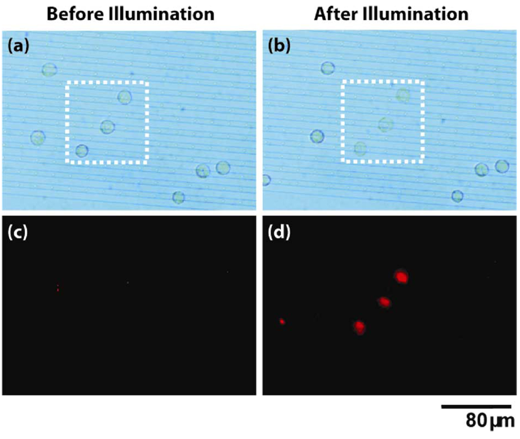
Fig. 6 demonstrates an example of this technique. Initially, a population of cells on the biased LOET device are in the absence of light [Fig. 6(a)]. The corresponding fluorescent image shows no PI fluorescence indicating that the cellular membrane is still intact [Fig. 6(c)]. The three cells in the dotted box are then illuminated. In the resulting bright field image, one can see the morphological change undertaken by the lysed cells [Fig. 6(b)]. The corresponding fluorescent image shows that each illuminated cell now fluoresces red, indicating membrane poration [Fig. 6(d)]. The fluorescence in the image is weak owing to the fact that the fluorescent molecules (i.e.,DNA) are no longer contained by the cell membrane and are free to diffuse.
Fig. 6. LOET Cell Lysis.
Top panels (a) and (b) show bright field images of HeLa cells in the LOET device before and after the three cells in the dotted box are illuminated. Bottom panels (c) and (d) show the corresponding PI fluorescence images. Not that only those cells which were illuminated are successfully lysed.
For most lysis applications, the contents of the lysed cell need to be collected for analysis. This is greatly facilitated by the use of on-chip microfluidic channels. Since the LOET is independent of the top substrate, it is quite straightforward to integrate channels (e.g., PDMS based) onto the device to extract lysed material.
C. Electrodeless Light-Induced Electroporation With OET
The last application of OET for cellular stimulation we will discuss is the use of OET for a recently reported electroporation technique called light-induced electroporation [31]. Here, we use the ability of the OET device to concentrate the electric field across an illuminated cell to electroporate individual cells in parallel [Fig. 3(c)]. This is achieved by a simple change in device bias. The technique seamlessly integrates with normal OET operation, allowing for parallel, single-cell electroporation and manipulation.
Upon light illumination in the OET device, the electric field is switched from the a-Si:H to the liquid layer. The electric field is concentrated in the liquid layer only in the illuminated regions. Therefore, if a cell is illuminated, the electric field is concentrated across it. Under normal OET operating conditions (0.2 kV/cm), the field is not strong enough to cause membrane poration. However, if the bias is altered so that the field the cell experiences exceeds approximately 1.5 kV/cm, the cell will porate. Thus, through a simple change in device bias, cells can be either manipulated or electroporated in parallel.
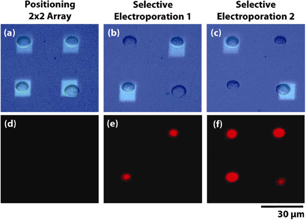
An example of this is shown in Fig. 7. (Adapted from [31]). Cells are initially arrayed into a 2 × 2 array at a low bias (0.2 kV/cm) [Fig. 7(a)]. The corresponding fluorescent image [Fig. 7(d)] shows no dye uptake indicating that manipulation in OET does not cause membrane poration. In the middle panel, two cells are selected and subjected to a field of 1.5 kV/cm [Fig. 7(b)]. The subsequent fluorescent [Fig. 7(e)] image shows that only those cells illuminated are electroporated. In the final panel, the remaining two cells are illuminated and subjected to the electroporation bias [Fig. 7(c)], resulting in the fluorescence of all four cells [Fig. 7(f)]. This demonstrates the ability of OET to perform parallel, single-cell electroporation and manipulation.
Fig. 7. Light-induced electroporation (Adapted from [31]).
Top row (a)–(c) shows bright field image of cells and optical pattern. Bottom row (d)–(f) shows the corresponding PI dye fluorescence. Cells are first arrayed using OET (0.2 kV/cm). OET manipulation bias does not cause electroporation. Two cells on the diagonal are then subjected to the electroporation bias (1.5 kV/cm) and, subsequently, fluoresce (image taken 5 min following electroporation bias). Finally, the remaining two cells are porated, resulting in the fluorescence of all cells.
V. DISCUSSION
Each of the three devices presented here has a variety of pros and cons associated with it depending on the user’s application and requirements.
The first device, consisting of OET integrated with microelectrodes, can achieve cell lysis and electroporation easily through the use of offchip electronics. By using OET to bring cells of interest to the electroporation/lysis site, fewer electrodes are necessary to achieve single-cell resolution which reduces device complexity and cost. In addition, since it uses normal OET, it affords full 2-D movement capabilities regardless of particle size (compared to the LOET where electrode size and spacing must be tuned to particle size). However, this device has a variety of cons. First, it requires a separate bias source for cellular stimulation and the device fabrication is more involved. Also, cells must be transported to the electrical stimulation area and cannot be porated/lysed in-situ. In addition, upon stimulation, cells are attracted to the exposed metal (via DEP) and often become so well adhered to the electrode that subsequent movement of the cell is difficult. This is a major issue for applications involving electroporation where the cell must be later extracted for culturing/analysis. This issue can be combated by altering electrode/cell interface by introducing barriers between the cell and electrode. Finally, due to the fact that this technique uses OET, the top substrate must be conductive and this makes integration with onboard fluidics for extraction of lysed material/cells more difficult. However, a basic process has been developed to integrate channels on to the traditional OET device by involving the lithographic patterning of SU-8 to define channel sidewalls on the OET bottom substrate and subsequent bonding of the top substrate by using a UV-curable epoxy [31]. This process allows one to use arbitrary top and bottom substrates; however, it is considerably more complex than traditional methods (e.g., PDMS based).
The second device discussed involves the use of LOET to affect single-cell lysis. The major benefit of this device is its ability to easily integrate with fluidic channels as no constraint is placed on the type of substrate required for the topside device. This is ideal for lysis applications where the lysate needs to be extracted for further analysis. In addition, unlike the first device, cells can be lysed in-situ so long as the electrode spacing is small enough. Another benefit is that the voltage necessary to achieve the lysis field (~ 10 kV/cm) is smaller (~ 10×) than that required to achieve the same field in the normal OET device. This is because the electrodes in the LOET device (~ 1 – 10 µm) can be spaced much closer together than in the OET device (~ 10 – 100 µm). This is because, in the OET device, the electrode spacing is equal to the gap spacing which must be at least as large as the diameter of the cell being studied (~ 10µm). Finally, unlike the first device, no additional electronic bias sources are necessary since the lysing field comes from the original LOET device bias. The issues with this device are that the LOET fabrication process is more complicated than the traditional OET device. In addition, if one wants to achieve full 2-D movement capability, the electrode spacing must be carefully designed to the particle size. This means that if one wants to manipulate/lyse cells of largely varying sizes, different devices/different electrode spacing must be used.
The final device involves the use of conventional OET to cause the electroporation of cells through a simple change in device bias. This device is the simplest of all three since there is no additional processing involved past the a-Si:H deposition and, like the LOET device, only one electrical bias source is needed. Also, like LOET, cells can be electroporated in-situ. In addition, full 2-D movement capability requires no special design considerations (unlike the LOET device). A drawback of this approach is that the applied electroporation/lysing voltage is higher than that required by the other devices by ~ 10×. As explained previously, this is because the electrode spacing in OET is dictated by the chamber gap which must be large enough to accommodate the cell diameter. Another issue, as discussed before, is that integration with fluidics is more involved than with the LOET device due to the reliance on a conductive top substrate. However, as mentioned before, processes do exist for the integration of channels with the OET device.
VI. CONCLUSION
Optoelectronic tweezers provides an interesting and powerful platform for parallel, single-cell manipulation. OET is ideal for this application as the optical power necessary for actuation is many orders of magnitude (~ 104 –106) less than that required by other optical manipulation techniques. The future of this device will be its integration with other lab-on-chip technologies. We have presented three devices to achieve parallel, single-cell lysis and/or electroporation with full OET/LOET manipulation capability. Each device has a variety of attributes which correspond to the user’s specific needs. These simple demonstrations realize the ability to integrate OET with other technologies in pursuit of a system capable of true parallel, single-cell manipulation and stimulation.
ACKNOWLEDGMENT
The authors would like to thank the UC Berkeley Cell Culture facility for providing the cells used in this study and the UC Berkeley Microlab where all devices were fabricated.
This work was supported by the Center for Cell Control, a National Institute of Health Nanomedicine Development Center under Grant PN2 EY018228. This paper was recommended by Associate Editor S. Bhattacharya.
Biographies

Justin K. Valley received the B.S. degree in electrical engineering from the University of Michigan, Ann Arbor, in 2006, the M.S. degree in electrical engineering from the University of California, Berkeley, in 2008, and is currently pursuing the Ph.D. degree in electrical engineering from the University of California, Berkeley.
His research interests include the areas of optical and biological microelectromechanical systems, microfluidics, and nonlinear optics.

Aaron T. Ohta (S’99–M’08) received the B.S. degree in electrical engineering from the University of Hawaii, Manoa, in 2003, the M.S. degree in electrical engineering from the University of California, Los Angeles, in 2004, and the Ph.D. degree in electrical engineering from the University of California, Berkeley, in 2008.
Currently, he is an Assistant Professor at the University of Hawaii. His research interests include microelectromechanical systems (MEMS) and bioMEMS.
Mr. Ohta is a recipient of a National Science Foundation Graduate Research Fellowship.

Hsan-Yin Hsu received the B.S. degree in electrical engineering from Purdue University, West Lafayette, IN, in 2005 and is currently pursuing the Ph.D. degree in electrical engineering from the University of California, Berkeley.
His research interest is in microelectromechanical systems, microfluidics, and optical systems for biomedicine applications.

Steven L. Neale received the MSci. and Ph.D. degrees in physics from the University of St. Andrews, Scotland, U.K., in 2002 and 2006, respectively.
He then was a Postdoctoral Researcher at St. Andrews in the microphotonics and photonic crystals research group before moving to the University of California, Berkeley. His research interests are the combination of microfabrication technology with micromanipulation techniques (including optical tweezing and dielectrophoresis) to produce new tools for the study of biology and nanotechnology.

Arash Jamshidi received the B.S. degree in electrical engineering from Simon Fraser University (SFU), Vancouver, BC, Canada, in 2005, and is currently pursuing the Ph.D. degree in electrical engineering at the University of California, Berkeley.
His research interests include nanotechnology, optoelectronics, and BioMEMS. Currently, he is working on optoelectronic tweezers (OET) applications in the nanoscale as part of the Integrated Photonics Laboratory (IPL) research group.

Ming C. Wu (S’82–M’83–SM’00–F’02) received the M.S. and Ph.D. degrees in electrical engineering from the University of California, Berkeley, in 1985 and 1988, respectively.
From 1988 to 1992, he was a member of the Technical Staff at AT&T Bell Laboratories, Murray Hill, NJ. From 1992 to 2004, he was a Professor in the Electrical Engineering Department at the University of California, Los Angeles. In 2004, he moved to the University of California, Berkeley, where he is currently Professor of Electrical Engineering and Computer Sciences and Co-Director of Berkeley Sensor and Actuator Center (BSAC). His research interests include (microelectromechanical and nanoelectromechanical systems), optofluidics, optoelectronics, nanophotonics, and biophotonics. He has published six book chapters, 140 journal and 300 conference papers, and holds 16 U.S. patents.
Prof. Wu is a member of the Optical Society of America. He was a Packard Foundation Fellow from 1992 to 1997, and received the 2007 Engineering Excellence Award from the Optical Society of America.
Footnotes
Color versions of one or more of the figures in this paper are available online at http://ieeexplore.ieee.org.
Contributor Information
Justin K. Valley, Email: valleyj@eecs.berkeley.edu, Electrical Engineering and Computer Science Department, Berkeley Sensor and Actuator Center, University of California, Berkeley, CA 94720 USA.
Aaron T. Ohta, Email: aohta@hawaii.edu, Electrical Engineering Department, University of Hawaii at Manoa, Honolulu, HI 96822 USA.
Hsan-Yin Hsu, Email: hsu@eecs.berkeley.edu, Electrical Engineering and Computer Science Department, Berkeley Sensor and Actuator Center, University of California, Berkeley, CA 94720 USA.
Steven L. Neale, Email: sln2@eecs.berkeley.edu, Electrical Engineering and Computer Science Department, Berkeley Sensor and Actuator Center, University of California, Berkeley, CA 94720 USA.
Arash Jamshidi, Email: arash@eecs.berkeley.edu, Electrical Engineering and Computer Science Department, Berkeley Sensor and Actuator Center, University of California, Berkeley, CA 94720 USA.
Ming C. Wu, Email: wu@eecs.berkeley.edu, Electrical Engineering and Computer Science Department, Berkeley Sensor and Actuator Center, University of California, Berkeley, CA 94720 USA.
REFERENCES
- 1.Junno T, Deppert K, Montelius L, Samuelson L. Controlled manipulation of nanoparticles with an atomic force microscope. Appl. Phys. Lett. 1995;vol. 66:3627–3629. [Google Scholar]
- 2.Li Y, Dalton C, Crabtree J, Nilsson G, Kaler KVIS. Continuous dielectrophoretic cell separation microfluidic device. Lab on a Chip. 2007;vol. 7:239–248. doi: 10.1039/b613344d. [DOI] [PubMed] [Google Scholar]
- 3.Fuchs AB, Romani A, Freida D, Medoro G, Abonnenc M, Altomare L, Chartier I, Guergour D, Villiers C, Marche PN, Tartagni M, Guerrieri R, Chatelain F, Manaresi N. Electronic sorting and recovery of single live cells from microlitre sized samples. Lab on a Chip. 2006;vol. 6:121–126. doi: 10.1039/b505884h. [DOI] [PubMed] [Google Scholar]
- 4.Roman G, Chen Y, Viberg P, Culbertson A, Culbertson C. Single-cell manipulation and analysis using microfluidic devices. Anal. Bioanal. Chem. 2007;vol. 387:9–12. doi: 10.1007/s00216-006-0670-4. [DOI] [PubMed] [Google Scholar]
- 5.Grier DG. A revolution in optical manipulation. Nature. 2003;vol. 424:810–816. doi: 10.1038/nature01935. [DOI] [PubMed] [Google Scholar]
- 6.Neuman KC, Nagy A. Single-molecule force spectroscopy: optical tweezers, magnetic tweezers and atomic force microscopy. Nat . Meth. 2008;vol. 5:491–505. doi: 10.1038/nmeth.1218. [DOI] [PMC free article] [PubMed] [Google Scholar]
- 7.Rao S, Bálint S, Cossins B, Guallar V, Petrov D. Raman study of mechanically induced oxygenation state transition of red blood cells using optical tweezers. Biophys. J. 2009;vol. 96:209–216. doi: 10.1529/biophysj.108.139097. [DOI] [PMC free article] [PubMed] [Google Scholar]
- 8.Ashkin A, Dziedzic JM, Yamane T. Optical trapping and manipulation of single cells using infrared laser beams. Nature. 1987;vol. 330:769–771. doi: 10.1038/330769a0. [DOI] [PubMed] [Google Scholar]
- 9.Dufresne ER, Grier DG. Optical tweezer arrays and optical substrates created with diffractive optics. Rev. Scientif. Instruments. 1998;vol. 69:1974–1977. [Google Scholar]
- 10.Mohanty SK, Rapp A, Monajembashi S, Gupta PK, Greulich KO. Comet assay measurements of DNA damage in cells by laser microbeams and trapping beams with wavelengths spanning a range of 308 nm to 1064 nm. Radiation Res. 2002;vol. 157:378–385. doi: 10.1667/0033-7587(2002)157[0378:camodd]2.0.co;2. [DOI] [PubMed] [Google Scholar]
- 11.Neuman KC, Chadd EH, Liou GF, Bergman K, Block SM. Characteriz. Photodamage to Escherichia coli Opt. Traps. 1999;vol. 77:2856–2863. doi: 10.1016/S0006-3495(99)77117-1. [DOI] [PMC free article] [PubMed] [Google Scholar]
- 12.Grigorenko AN, Roberts NW, Dickinson MR, Zhang Y. Nanometric optical tweezers based on nanostructured substrates. Nat Photon. 2008;vol. 2:365–370. [Google Scholar]
- 13.Xiaoyu M, Lin LY. Trapping and manipulation of biological particles through a plasmonic platform. IEEE J. Sel. Topics Quantum Electron. 2007 Nov./Dec.vol. 13(no. 6):1655–1662. [Google Scholar]
- 14.Lee SE, Liu GL, Kim F, Lee LP. Remote optical switch for localized and selective control of gene interference. Nano Lett. 2009;vol. 9:562–570. doi: 10.1021/nl802689k. [DOI] [PMC free article] [PubMed] [Google Scholar]
- 15.Chiou PY, Ohta AT, Wu MC. Massively parallel manipulation of single cells and microparticles using optical images. Nature. 2005;vol. 436:370–372. doi: 10.1038/nature03831. [DOI] [PubMed] [Google Scholar]
- 16.Ohta AT, Chiou PY, Han TH, Liao JC, Bhardwaj U, McCabe ERB, Yu F, Sun R, Wu MC. Dynamic cell and microparticle control via optoelectronic tweezers. J. Microelectromechan. Syst. 2007;vol. 16:491–499. [Google Scholar]
- 17.Hsu HY, Ohta AT, Chiou PY, Jamshidi A, Wu MC. Phototransistor-based optoelectronic tweezers for cell manipulation in highly conductive solution; presented at the 14th Int. Conf. Solid-State Sensors, Actuators and Microsystems; Lyon, France. 2007. [Google Scholar]
- 18.Ohta AT, Chiou P-Y, Phan HL, Sherwood SW, Yang JM, Lau ANK, Hsu H-Y, Jamshidi A, Wu MC. Optically controlled cell discrimination and trapping using optoelectronic tweezers. IEEE J. Sel. Topics Quantum Electron. 2007 Mar./Apr.vol. 13(no. 2):235–243. [Google Scholar]
- 19.He HQ, Chang DC, Lee YK. Using a micro electroporation chip to determine the optimal physical parameters in the uptake of biomolecules in HeLa cells. Bioelectrochem. 2007 May;vol. 70:363–368. doi: 10.1016/j.bioelechem.2006.05.008. [DOI] [PubMed] [Google Scholar]
- 20.Khine M, Lau A, Ionescu-Zanetti C, Seo J, Lee LP. A single cell electroporation chip. Lab on a Chip. 2005;vol. 5:38–43. doi: 10.1039/b408352k. [DOI] [PubMed] [Google Scholar]
- 21.Stevenson D, Agate B, Tsampoula X, Fischer P, Brown CTA, Sibbett W, Riches A, Gunn-Moore F, Dholakia K. Femtosecond optical transfection of cells: Viability and efficiency. Opt. Expr. 2006 Aug.vol. 14:7125–7133. doi: 10.1364/oe.14.007125. [DOI] [PubMed] [Google Scholar]
- 22.Yamada M, Kobayashi J, Yamato M, Seki M, Okano T. Millisecond treatment of cells using microfluidic devices via two-step carrier-medium exchange. Lab on a Chip. 2008;vol. 8:772–778. doi: 10.1039/b718281c. [DOI] [PubMed] [Google Scholar]
- 23.Adamo A, Jensen KF. Microfluidic based single cell microinjection. Lab on a Chip. 2008;vol. 8:1258–1261. doi: 10.1039/b803212b. [DOI] [PubMed] [Google Scholar]
- 24.Schilling EA, Kamholz AE, Yager P. Cell lysis and protein extraction in a microfluidic device with detection by a fluorogenic enzyme assay. Anal. Chem. 2002;vol. 74:1798–1804. doi: 10.1021/ac015640e. [DOI] [PubMed] [Google Scholar]
- 25.Carlo DD, Jeong K-H, Lee LP. Reagentless mechanical cell lysis by nanoscale barbs in microchannels for sample preparation. Lab on a Chip. 2003;vol. 3:287–291. doi: 10.1039/b305162e. [DOI] [PubMed] [Google Scholar]
- 26.Lee C-Y, Lee G-B, Lin J-L, Huang F-C, Liao C-S. Integrated microfluidic systems for cell lysis, mixing/pumping and DNA amplification. J. Micromechan. Microeng. 2005:1215. [Google Scholar]
- 27.Kaustubh RR, Arnold G, III, Alfred V, Vasan V. Investigation of laser-induced cell lysis using time-resolved imaging. Appl. Phys. Lett. 2004;vol. 84:2940–2942. [Google Scholar]
- 28.Gao J, Yin X-F, Fang Z-L. Integration of single cell injection, cell lysis, separation and detection of intracellular constituents on a microfluidic chip. Lab on a Chip. 2004;vol. 4:47–52. doi: 10.1039/b310552k. [DOI] [PubMed] [Google Scholar]
- 29.Lin Y-H, Lee G-B. An optically induced cell lysis device using dielectrophoresis. Appl. Phys. Lett. 2009;vol. 94:033901. [Google Scholar]
- 30.Ohta AT, Jamshidi A, Pauzauskie PJ, Hsu H-Y, Yang P, Wu MC. Trapping and transport of silicon nanowires using lateral-field optoelectronic tweezers; Proc. Conf. Lasers and Electro-Optics/Quantum Electronics and Laser Science Conf. Photonic Applications Systems Technologies; 2007. p. CThGG5. [Google Scholar]
- 31.Valley JK, Neale S, Hsu H-Y, Ohta AT, Jamshidi A, Wu MC. Parallel single-cell light-induced electroporation and dielectrophoretic manipulation. Lab on a Chip. 2009;vol. 9:1714–1720. doi: 10.1039/b821678a. [DOI] [PMC free article] [PubMed] [Google Scholar]


