

Abstract
Positron emission tomography (PET) is a tool for metabolic imaging that has been utilized since the earliest days of nuclear medicine. A key component of such imaging systems is the detector modules—an area of research and development with a long, rich history. Development of detectors for PET has often seen the migration of technologies, originally developed for high energy physics experiments, into prototype PET detectors. Of the many areas explored, some detector designs go on to be incorporated into prototype scanner systems and a few of these may go on to be seen in commercial scanners. There has been a steady, often very diverse development of prototype detectors, and the pace has accelerated with the increased use of PET in clinical studies (currently driven by PET/CT scanners) and the rapid proliferation of pre-clinical PET scanners for academic and commercial research applications. Most of these efforts are focused on scintillator-based detectors, although various alternatives continue to be considered. For example, wire chambers have been investigated many times over the years and more recently various solid-state devices have appeared in PET detector designs for very high spatial resolution applications. But even with scintillators, there have been a wide variety of designs and solutions investigated as developers search for solutions that offer very high spatial resolution, fast timing, high sensitivity and are yet cost effective. In this review, we will explore some of the recent developments in the quest for better PET detector technology.
Positron emission tomography—some of the basics
The use of imaging to obtain metabolic information is an area of considerable development. In a review article by Cherry (2004), the many different imaging modalities being utilized to acquire such data and the kinds of studies being performed are well summarized. One of the major imaging modalities discussed in Cherry’s review article is positron emission tomography (PET), which utilizes radioactive tracers to make images of the distribution of labeled molecules in vivo. Since it is a tracer approach, the introduction of the labeled compound used for imaging does not alter the biological state of the subject. As discussed in Cherry (2004), the notion of in vivo molecular and genomic imaging (or metabolic imaging as used in this review) is not new, but is rapidly growing for both human and pre-clinical applications. Here, we will focus on the basic detector technologies being applied to the area of PET and begin with a brief review of some of the basic concepts of PET imaging.
Excluding single photon emission tomography (SPECT) systems with 511 keV rated parallel hole collimators, all PET systems utilize coincidence detection of the annihilation photons from positron decay (figure 1). Since the paired gamma rays from the annihilation of the positron are anti-parallel, the detection of the gamma rays determines a line of response (LOR) along which the annihilation took place. Typically, scanners are designed around rings of detectors (figure 2). The coincidence is determined by imposing an acceptance window on the time difference between detection of the two events (typically, a window a few nanoseconds wide). There are three major types of events that can cause coincidence events (figure 3). A true coincidence occurs when a single positron annihilates and both of the gamma rays are detected without either of them scattering in the object being scanned. A scattered coincidence occurs when one or both of the 511 keV annihilation photons from a single positron decay scatter in the object being scanned. This is a true coincidence since it came from single positron annihilation, but the resulting LOR will be misplaced, resulting in reduction of spatial resolution and image contrast. The third type of coincidence is a random, or accidental, coincidence. This event occurs when two positrons annihilate and one gamma ray from each annihilation is detected. If the two events occur close enough in time, then the tomograph electronics will register the event as a coincidence (or a prompt event). However, such randoms are distributed uniformly in time (figure 1) and only the portion of random events included in the prompt window ‘contaminates’ the primary data set.
Figure 1.

Coincidence detection. When a positron annihilates, two 511 keV gamma rays are emitted. If both gamma rays interact in a pair of detectors, the events will be recorded at approximately the same time, in coincidence. If a time spectrum is generated (the number of events versus the time between detector 1 and detector 2 responding), a peak is formed. This peak is usually termed the coincidence or prompt peak. During acquisition, a delayed time window can be used to measure random coincidence events.
Figure 2.

Typical PET system geometry. The object being scanned is usually surrounded by rings of detectors. Each detector acts as a single event detector (records single gamma-ray events). When single events occur within a short time of each other, they are considered in coincidence and saved as a prompt event. The time difference to be considered in coincidence is usually a few nanoseconds.
Figure 3.

The three types of coincidence events. True coincidences occur when the two gamma rays from single positron annihilation are detected and neither gamma ray undergoes Compton scattering. Scatter coincidences are true coincidences where one or both of the gamma rays undergo Compton scattering before being detected. Random coincidences occur when only one gamma ray from two independent positron annihilations are detected within the timing window of the coincidence system.
The prompt data provide a data set consisting of LORs along which it is assumed that an annihilation event occurred. If the system has very high timing resolution (<1 ns), then we have some information about where along the LOR the event occurred. For example, a time-of-flight (TOF) resolution of 600 ps allows us to constrain the annihilation position to a roughly Gaussian-shaped region along the LOR with a full width at half-maximum of ~9 cm. If all other parameters are equal, a TOF system can provide a higher signal-to-noise ratio (SNR) than a non-TOF system. In addition to determining if two events are within a timing acceptance window (if they are prompt or delayed events), the system electronics also apply energy acceptance criteria, reducing some of the scattered events. During image reconstruction, corrections can be made for both randoms and scatter. Randoms can be determined in a scanner by either sampling the randoms for each LOR by applying a timing acceptance window that is delayed from the prompt window (accepting events that are not true coincidence or scattered events—figure 1) or measuring the single event rates in each detector unit and calculating the randoms. Scatter can be estimated by one of several approaches. Details on PET image reconstruction can be easily found in the literature and text books (e.g. Lewellen and Karp (2004)).
The role of the detector is to stop an emitted gamma ray and produce a signal that the downstream electronics can utilize. This signal needs to carry information about how much energy was deposited in the detector, information about the physical location of the event in the detector array and timing information (when did the event occur). To fulfill this role, the ideal detector would
have high stopping power (high probability that a 511 keV gamma ray will be totally absorbed by the detector),
have high spatial resolution (ability to determine the interaction location of the gamma ray in the detector to a small spatial volume),
have very good energy resolution (to reject scattered events),
have very high timing resolution and
be inexpensive to produce.
To further complicate an ideal detector wish list, the attributes that should be emphasized depend on the final target application. For simplicity, I like to group applications into three main categories: (1) pre-clinical (e.g. small animal) imaging, (2) dedicated neuro-imaging and (3) whole-body imaging. For all three categories, there is a need to strive for higher sensitivity. For pre-clinical imaging, the parameter getting the most attention is spatial resolution with newer designs striving to achieve <1 mm3 isotropic volume resolution. Timing resolution is not as important for pre-clinical imaging since the count rates are such that randoms rates are generally low and there is no current expectation of obtaining TOF resolution sufficiently low to be useful for such small volumes. For neuro-imaging, the spatial resolution target can be relaxed (perhaps ~3 mm3). Many brain imaging applications want both high spatial resolution and good dynamic imaging, and thus sensitivity is particularly important. Sensitivity is also important if effects such as non-collinearity of annihilation gamma rays are to be addressed in the image reconstruction algorithm. Further, timing resolution is important for randoms’ rejection. To date, TOF is not a big issue in such dedicated systems given the size of the objects being scanned and the current state-of-the-art in TOF capabilities (current TOF resolution does not improve the SNR significantly in brain-sized objects). Body imaging is a bit different story. Current commercial systems have crystal cross section dimensions as small as 4 × 4 mm2. The realities of dose limitations and the number of gamma rays detected (and hence the variance due to the photon statistics) make going to smaller detector dimensions for body imaging generally not a goal in most detector designs. Current systems cannot generally reach their spatial resolution limits due to the amount of variance in the images. Thus, one of the current major areas of development for body systems is that of pushing the TOF resolution to achieve an improvement in the final signal-to-noise ratio in the images. It should be no surprise that the ideal detector is yet to be developed for any of these applications and is an area of very active research.
The goal of this review is to highlight many of these areas of development. Given the many laboratories and companies engaged in such development, I will not attempt to catalog all of the many investigators and innovative solutions connected with PET detectors. It is a very active and innovative area of research. Instead, I have chosen specific examples of many of the different technologies and solutions being worked on. Even then, the technologies I have included are not all inclusive but represent those that, in my opinion, have received the most interest in the literature and recent scientific meetings. I apologize in advance to those whose efforts are not directly discussed and those technologies not included. In preparing this narrative, I have assumed that the reader is familiar with detector technologies, but might not be working with PET imaging systems. Perhaps the best place to begin is with scintillator-based systems since this is what leads to the development of the first PET scanners and is still the dominant detector type used in both commercial and laboratory-built systems.
Basic scintillator detectors
Early PET scanners were based on the use of NaI(Tl) scintillators coupled to photomultiplier tubes (PMT). Scintillator-based designs remain the most common primary detector for PET scanners and are a very active area of development. Table 1 lists some of the properties of scintillators found in many PET detector designs. Ideally, a scintillator should be fast, dense, have high light output and be cheap to produce. There are no ideal scintillators as of yet, but it is another active area of development. While table 1 is not exhaustive, it does illustrate the advantages and disadvantages of scintillators found in current detector designs.
Table 1.
Properties of some scintillators used in PET detectors. Note that some of these specifications are subject to change as developers change dopants and trace elements in the scintillator growth. For example, the light output, peak wavelength, decay time and density for LYSO and LFS will vary somewhat for different versions of the basic scintillator.
| NaI(Tl) | BaF2 | BGO | LSO | GSO | LYSO | LaBr3 | LFS | LuAP | LuI3 | |
|---|---|---|---|---|---|---|---|---|---|---|
| Effective atomic no. (Z) | 51 | 54 | 74 | 66 | 59 | 60 | 47 | 63 | 65 | 60 |
| Linear attenuation coeff. (cm−1) | 0.34 | 0.44 | 0.92 | 0.87 | 0.62 | 0.86 | 0.47 | 0.82 | 0.9 | ~0.56 |
| Density (gm cm−3) | 3.67 | 4.89 | 7.13 | 7.4 | 6.7 | 7.1 | 5.3 | 7.3 | 8.34 | 5.6 |
| Index of refraction | 1.85 | – | 2.15 | 1.82 | 1.85 | 1.81 | 1.88 | 1.78 | 1.95 | |
| Light yield (% NaI(Tl)) | 100 | 5 | 15 | 75 | 30 | 80 | 160 | 77 | 16 | 190 |
| Peak wavelength (nm) | 410 | 220 | 480 | 420 | 430 | 420 | 370 | 430 | 365 | 470 |
| Decay constant (ns) | 230 | 0.8 | 300 | 40 | 65 | 41 | 25 | 35 | 18 | 30 |
| Hydroscopic | Yes | Slight | No | No | No | No | No | No | No | Yes |
The first systems were single crystals mounted on individual PMTs. However, as designs began to reduce the crystal cross section size (to obtain improved spatial resolution), alternatives to the one-on-one coupling (one crystal per PMT) had to be developed. The limitations of continuing the one-on-one schemes included the cost (numbers of PMTs), the lack of very small PMTs, the number of electronics channels and problems of packing the PMTs together, given the physical size of the glass envelopes of the PMTs. Two basic schemes emerged (figure 4). One was developed as a consequence of the use of BGO in PET scanners. As seen in table 1, BGO has the advantages of high stopping power but has low light output compared to NaI(Tl). To offset the light output, ‘block designs’ were developed. These designs were either an array of individual crystals or a block of scintillator with saw cuts (Casey and Nutt 1986, Wong et al 1993). In either case, the goal was to channel the light to produce the desired light response function (LRF) to allow decoding of the array with a small number of PMTs. Typically, four PMTs are placed over the crystals in a rectangular pattern and ratios are formed from the PMT signals to provide a transverse and axial position signal as indicated in figure 5. An example of plotting numbers of events versus the transverse and axial position values is shown in figure 6—a map of the response from a 6×6 array of BGO crystals viewed by four PMTs. This basic approach is still being utilized, but the details have evolved in a variety of design approaches as will be discussed below.
Figure 4.

The major crystal/PMT decoding geometry options developed for current PET scanners. The continuous ‘Anger’ approach uses an array of PMTs to decode a large, continuous crystal or array of crystals. The ‘block detector’ uses four PMTs to decode an array of crystals with various combinations of reflectors and surface treatments between the crystals.
Figure 5.

Example of a typical block detector decoding scheme. In this case, a 6 × 6 array is decoded by four PMTs. The PMT signals (A, B, C and D) are summed to determine the energy signal (E) as well as two position-dependent signals (X, Z). X and Z are used to form maps of the crystal locations.
Figure 6.
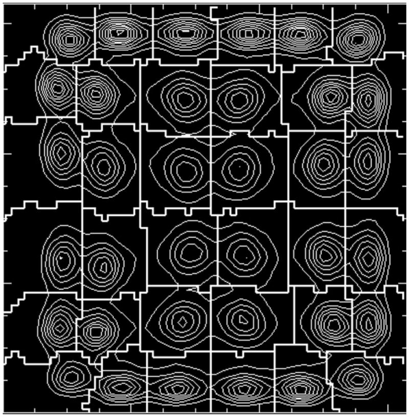
A block map of a 6 × 6 BGO crystal array viewed by four PMTs. The relative light output is indicated by the iso-count curves. The heavy white lines indicate what regions will be assigned to each crystal position.
The other major decoding scheme was to adapt the concept of large crystals viewed by an array of PMTs (the Anger camera approach) (Karp et al 1990, 2003, Muehllehner and Karp 1986). This approach was originally developed for use with NaI(Tl) scintillators since it requires good light output. However, the low stopping power of NaI(Tl) was a disadvantage and is no longer in use for PET detector development for human systems, although at least one group is looking at NaI(Tl) detectors for small animal PET applications. The basic concepts developed have continued to be utilized. For example, one commercial PET scanner developed a panel consisting of an array of GSO crystals coupled to a light pipe and then viewed by an array of PMTs in a manner very similar to the NaI(Tl) panels developed for PET imaging (Surti and Karp 2004) and then extended that design to use LYSO in place of GSO (Surti et al 2007).
Let us consider some of the complications with either design in terms of gamma-ray interactions within the detector. Figure 7 depicts some of the possible issues that can degrade the spatial resolution in a pixelated detector. Ideally, the spatial resolution of the scanner should be related to approximately half the width of an individual crystal. There are several compounding factors that limit the resolution achievable in a real detector module. One is scatter within the detector. In most scintillators used in PET, the probability of a photoelectric interaction (total absorption) on the first interaction is less than 50% for 511 keV gamma rays (e.g. BGO is 43%, LSO is 34% and NaI(Tl) is 18%). If the crystals are very short, a gamma ray that Compton scatters in the detector will often exit without a second interaction. This design option has been used in some pre-clinical PET scanners to reduce resolution loss (e.g. Miyaoka et al (2005)). Otherwise, to improve overall sensitivity, the crystals are usually long enough so that a large number of gamma rays that Compton scatter within the detector array are subsequently absorbed with a photoelectric interaction. The resulting multiple points of light emission within the array lead to errors in decoding the crystals (the assignment of map partitions as illustrated in figure 6 assumes a single point of light emission). Investigators have developed some solutions for this problem including estimates of the detector response function in the image reconstruction process (e.g. Alessio et al (2004), Staelens et al (2004), Lee et al (2004), Derenzo (1986)). Penetration of a gamma ray from an oblique angle into the array can also lead to loss of spatial resolution. Most systems assign a LOR based on some small distance from the front edge of a given crystal that has been assigned as the source of the event. The fact that the event occurred deeper in the crystal means that the LOR is not correct (figure 7). One solution that is a very active area of development is to add the ability to determine how deep in the crystal an event actually occurs (depth of interaction or DOI). Further discussion of DOI is included later in this review. The general problem of statistical uncertainty due to the amount of light emitted in the gamma-ray interactions and collected by the photosensors further degrades the crystal identification process. In linear positioning algorithms such as those presented in figures 5 and 6, the result is a loss of resolution due to misidentification of the crystal. However, an alternative is to use statistical estimation techniques to determine the point of interaction in the crystal array rather than linear algorithms (Parra and Barrett 1998, Budinger 1998, Joung et al 2000, 2002). These techniques can include models for all of the degradation effects and can be implemented at either the detector level or as part of the image reconstruction process.
Figure 7.

Some of the factors that degrade spatial resolution in a pixelated detector array. Photon penetration results in incorrect assignment of the line of response in a scanner if depth-of-interaction (DOI) is not able to be measured. Scatter within the detector results in degraded crystal identification. Statistical uncertainty reflects errors in the decoding process due to the statistics of the amount of light collected.
In a similar manner, there are several basic detection issues that degrade the spatial resolution achievable with a continuous (i.e. non-pixelated) detector. The light response function can vary in shape dramatically for all three of the reasons shown in figure 8. The statistics of light emission and collection as well as the distortions in the shape of the LRF due to reflections from the sides and back surfaces work to degrade decoding of the position of the event. Just as in the pixelated case, scatter within the detector will also distort the LRF. And, again as in the pixelated detector, depth of interaction plays a role. The shape of the LRF can depend strongly on the DOI if the crystal is thick enough and the light reflections are controlled (e.g. putting a black absorber on the edges to enhance the effect or using a properly designed retroreflector). This DOI dependence on the LRF can be either a hindrance (degrade spatial resolution) or an added parameter to extract and utilize to address the parallax problem. We will discuss DOI approaches in more detail later in this review.
Figure 8.

Some of the factors that degrade spatial resolution in a continuous crystal detector design. The light output and response function reflect both light sampling and the statistics of the amount of light collected. Scatter in the detector and depth of interaction (and the resulting change in the light response function—LRF) generally lead to a loss of spatial resolution due to the changes in the LRF.
What are the major areas of development for scintillator-based detector designs? One obvious area is the search for new scintillators. The advent of LSO (followed by other lutetium compounds—see table 1 for a few of them) provided designers with a series of fast, bright, dense scintillators. These lutetium scintillators are more expensive than NaI(Tl) or BGO to grow, but they do offer performance options unobtainable with the older scintillators. One option is to use the increased light output to decode more crystals per PMT. We have already mentioned the panels of GSO and LYSO crystals using an array of PMTs. Even with the ‘conventional’ block design with four effective PMTs, the use of these brighter scintillators has allowed the use of larger arrays of smaller crystals (e.g. Jakoby et al (2007)). An illustration of the impact of these brighter scintillators on block decoding capabilities is provided in figure 9, which depicts a profile through a block map like figure 6 for four different scintillators. The ‘peak-to-valley’ ratio improves with more light, and this allows decoding more crystals per block.
Figure 9.

Illustration of the impact of brighter scintillators on the ability to decode crystals in a block. The profiles are through block maps similar to figure 6 and illustrate that the best decoding (valleys between the peaks closer to 0) is achieved with the brightest scintillator (LuI3) and scales with scintillator brightness. Data courtesy of William Moses.
With the advent of improved electronics and better performance PMTs, time-of-flight (TOF) PET has also reappeared as a commercial product (Surti et al 2007). Modern commercial TOF systems run with timing resolutions of 580—700 ps, about the same timing as achieved in the 1980s with BaF2 (Lewellen 1998), but now with much higher stopping power so that the TOF can be utilized without a major compromise of overall detection efficiency (Moses 2007). Work is also being done on yet brighter scintillators such as LaBr3 and CeBr3 as options for TOF PET with timing resolutions on the order of 300 ps or better (Kuhn et al 2006, Glodo et al 2007). Here, the challenge is the lower stopping power of the scintillator which will require longer crystals to achieve the same overall stopping power of the LYSO and LSO scanners. Longer crystals for a fixed ring diameter usually mean degradation of the radial resolution due to parallax. The fix for this problem brings us back to DOI and how to measure it. But first, we should take a look at changes in photodetectors since the new devices now available to investigators play a large role in the ability to make practical DOI detectors.
Advances in photodetectors
The ‘workhorse’ for scintillation detectors has been the photomultiplier tube (PMT). They are very high gain (typically ~×106), low noise, fast response and relatively low cost. They normally require bias voltages of 800–1200 volts. As noted earlier, the size of the PMTs and their glass envelopes limited the ability to make high spatial resolution detectors with one-on-one (one crystal to one PMT) coupling and lead to the evolution of the block detector concept (figure 4). PMTs have improved and, in particular, have made progress on the problems of the bulk of the devices (the overall size and the size of the vacuum envelope around the photocathode). The detector designer can now utilize PMTs that have multiple dynode chains or channels (effectively multiple PMTs) inside a common vacuum envelope. Photonis, Burle and Hamamatsu, for example, offer PMTs with 4–256 channels in a variety of package sizes. Each channel provides an essentially independent photodetector. For example, the Hamamatsu H9500 provides 256 channels, each one providing a 3 × 3 mm2 photodetector. A few of the many multichannel PMTs are shown in figure 10. These multi-channel PMTs as well as a series of other position-sensitive PMTs (e.g. cross anode) opened up new possibilities in detector designs. Now, designers have less dead space between the active areas of the PMT channels, the ability of using a larger number of channels to view either an array of crystals or a crystal ‘slab’, and more compact PMT housing overall. We will see how some of these PMTs have been used in several detector designs. Work continues to improve PMTs, particularly in terms of the timing response for TOF applications with timing resolutions on the order of 300 ps with LSO, and LaBr3 being reported for PET style detectors (Kuhn et al 2006, Glodo et al 2007, Moses 2007).
Figure 10.
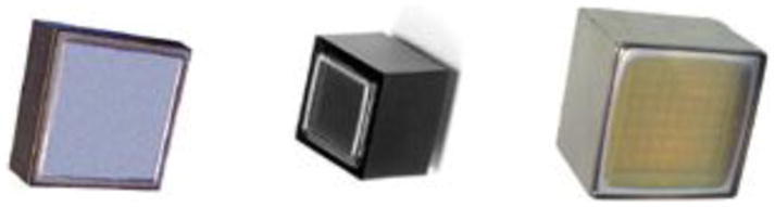
Examples of multi-channel PMTs from Burle (left), Hamamatsu (center) and Photonis (right). Such devices come in a variety of sizes with 4–256 channels and have been one of the key components in new PET detector designs.
However, much of the current excitement in new detector designs is centered around alternatives to PMTs. The desire to have options for one-on-one coupling with small crystal cross sections, the use of photodetectors on multiple surfaces of a scintillator array or slab, to further reduce the volume of the photosensor and to have detectors that can operate within magnetic fields led investigators to consider various forms of solid-state photodetectors. One of the first to be used were silicon PIN diodes. These devices are compact, have high quantum efficiency (ranging from 10% to 60% for various different devices) and can be used in magnetic fields. The downside is that they have a gain of unity, requiring low noise preamplifiers for signal readout, and they do not have good enough time resolution for TOF PET applications nor many other PET applications where random rates are a concern. The devices continue to improve with lower dark currents and the availability of fine pitched arrays (figure 11) and have been used in some PET detector designs (Frach et al 2004, Safavi-Naeini et al 2007), but the timing resolution and SNR concerns have limited their use by most developers of PET systems. There have been hybrid designs that use both PIN diodes and photomultiplier tubes as we shall see when we discuss depth of interaction.
Figure 11.
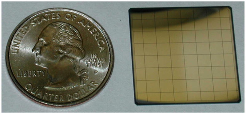
Example of a silicon PIN diode 64n element array from RMD with 2.45 mm pixels. Such devices are stable, have become cost effective and can be used in magnetic fields. However, they have unity gain and require low noise preamplifiers and do not have good enough time resolution for TOF PET applications.
Another device that has been popular is the avalanche photodiode (APD). This device has the advantage over silicon PIN diodes that it has higher gain (~102–103) and has faster timing (on the order of 1 ns), well suited for non-TOF PET applications. While the gain is higher than PIN diodes, APDs still require preamplifiers, but they do not need to be ultralow noise devices. The gain is a function of the bias voltage (as in a PMT) and can run from 200 to 2000 volts depending on the device and the application. One complication is that the gain is temperature sensitive, and gain shifts can be significant with a 1 or 2° (Celsius) change. As with PIN diodes APDs can be found in single packages or as arrays (figure 12). More recently, position-sensitive planar APDs (PS-APD) have been produced, again in a variety of sizes (figure 12). These devices use signals from the four corners of the device to determine the position of an event much like the technique used in the original block detectors. One advantage of PS-APDs is that the number of data channels in the electronics (preamplifiers, ADCs, etc) are reduced compared to discrete arrays in most applications. However, the noise in PS-APDs is generally worse than standard APDs. In general, the SNR of current photodiode devices is a potential limitation that has to be considered for any PET detector design.
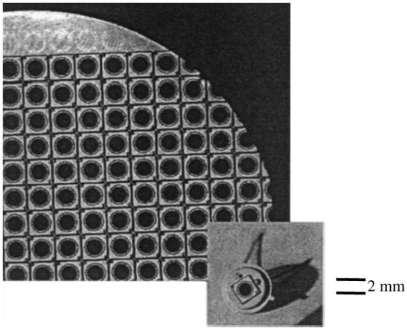
Figure 12.

Examples of avalanche photodiodes. Devices are available in a variety of packages in both single pixel and arrays and are being used in several different PET detector designs. Such devices have reasonable gains (~102) and can be used in magnetic fields.
One of the newest devices to appear is the Geiger-mode APD or silicon photomultiplier (Herbert et al 2007, Britvitch et al 2007, McElroy et al 2007, Musienko et al 2007, Renker 2007). These devices are under active development by a number of companies (more than nine were known to the author when this review was prepared) and go by a variety of names. For this review, we will term all such devices SiPMs. Because there is such rapid development going on for these devices, performance parameters are also rapidly changing. The basic device is built around a series of APD micro-cells (figure 13). Each cell is an independent Geiger-mode detector that is biased such that when a photon interacts in the cell, it discharges. Each cell is connected to the bias voltage by an individual resistor which results in the cell discharge being quenched. The cells are then connected to a common output. Ideally, a SiPM should produce the same size and shape of a current pulse from each cell, making each cell a digital detection device (on or off). When coupled to a scintillator, the hundreds to thousands of light photons that are emitted by the scintillator interact in a large number of the micro-cells. The result is an output pulse similar to that seen in PMTs (figure 14). Gains for typical devices range from 105 to 107 and produce a signal of several millivolts on a 50 ohm load, making it very similar to PMTs. The bias voltage required again varies between different devices, but typically is between 30 and 150 volts. The devices should be capable of good to excellent timing resolution. Time resolutions of 100 ps have been obtained for single photons, and current devices tested with scintillators have achieved 250–500 ps timing resolution with high light output, fast scintillators. Like most semiconductor devices, SiPMs are susceptible to thermal noise. The dark count rate is due to thermally generated electrons, leading to an avalanche process in one of the micro-cells. While the dark count rate can be quite high (i.e. >300 kHz mm−2), because each micro-cell is independent and the noise pulse is very narrow (i.e. <50 ns), the noise signal can be removed by using a simple low energy threshold. Furthermore, for lutetium-based scintillators with signal integration times on the order of 100 ns, noise due to dark counts during signal integration will rarely exceed the single photoelectron value. One limitation of such devices is that current designs have relatively large capacitance per unit area, which leads to problems in scaling up such devices to large detection areas (greater than about 3 × 3 mm2 active areas in a single device with current devices).
Figure 13.
Example of a Geiger-mode avalanche photodiode or silicon photomultiplier (SiPM). A series of micro APD cells are connected via the resistance in the surrounding silicon. When a photon interacts in a cell, it discharges and is then quenched via the resistance coupling it to the voltage supply. When coupled to a scintillator, the many light photons that are emitted by the scintillator cause many cells to fire producing an analogue-like output signal similar to that seen in PMTs.
Figure 14.

Example of a 511 keV energy spectrum from a SiPM. In this case, a Zecotek MAPD device was coupled to a 2 × 2 × 12 mm3 LFS-3 crystal (also from Zecotek).
Note in figure 13 that there is a dead space (as far as light photon detection) around each micro-cell. The dead space is needed to reduce optical cross talk between micro-cells (preventing neighboring cells from firing spuriously) and to provide electrical isolation between the micro-cells (except for the needed resistance and capacitance to provide the needed quenching of the current once a cell fires). The amount of dead space required depends on the details of the device design (Sadygov et al 2006). To achieve good linearity, a large number of micro-cells is needed to avoid saturation of the device and multiple interactions in the same micro-cell. However, as the numbers of cells increase by using smaller diameter micro-cells, the amount of dead space also increases, reducing the overall quantum efficiency over the area of the device. So, detector designers have to choose between linearity and quantum efficiency and determine the best compromise for their detector. Current devices can offer a range of microcells mm−2 of 100–10 000. These devices can also be made as either p-silicon on an n-substrate (and are sensitive to blue light) or as n-silicon on a p-substrate (and are sensitive to green light). In either case, the process is typically a CMOS fabrication technique much as is used for integrated circuits and offers the possibility of low cost as well as a wide range of pixel sizes (the collection of micro-cells within a device) and fine pitch arrays. The devices can be used in magnetic fields and samples have been tested in fields up to 15 Tesla without showing any degradation. Manufacturers are currently offering both p–n and n–p variants, and some arrays have also been shown. The interest in these devices is high, and many groups are experimenting with detector designs built around the expectation of low cost, high performance SiPM arrays.
DOI approaches with scintillators
A major area of development for the last several years has been that of measuring DOI in order to reduce parallax errors and maintain good sensitivity. DOI also allows smaller detector rings since the parallax corrections reduce the loss of spatial resolution with the radial position. The initial work has been primarily in scintillator-based detectors although we will return to DOI when we discuss recent progress in non-scintillator-based detector systems. One of the first approaches was to utilize pulse shape discrimination (PSD) and scintillators with different decay times, as illustrated in figure 15 (Costa et al 1986, Dahlbom et al 1997, Seidel et al 1999, Chung et al 2004, Braem et al 2007a, Yong et al 2007). Since the different decay times result in different pulse shapes, once can use several techniques to discriminate which scintillator is the source of the light (e.g. simply setting different windows in the time spectra). Many combinations of scintillators have been used including LSO, GSO, LuAP and BGO. Some designs use different dopants in LSO, LYSO or GSO to change the decay times enough to utilize the pulse shape discrimination approach. The PSD approach has been used in several scanners—both University and commercially developed. Most applications of such detectors have been for pre-clinical and dedicated brain scanners.
Figure 15.
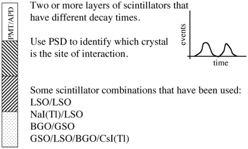
Pulse shape discrimination based depth-of-interaction detector designs. The concept is to use two or more layers of crystals that have different light decay times. A pulse shape analyzer can then be used to separate the light from each layer based on its different decay times (and resulting pulse shapes).
One of the drawbacks with the PSD approach has been the cost of fabrication of the detector modules due to the mechanical operations to assemble and match the needed crystals. Another complication is limitations on the system timing resolution parameters due to the different decay times, making such approaches not attractive for TOF detector designs. Another problem (in fact, a general problem for most DOI designs) is that of scattering within the crystal array resulting in light being produced from more than one of the scintillators, reducing the DOI accuracy. As we will discuss a bit later, there are methods being developed to improve the estimation of the point of first interaction by including appropriate knowledge about the physics of such multiple interactions and the geometry of the scanning system.
Recently, investigators at UC Davis reported on a new approach to the PSD detector design at the 2007 IEEE Nuclear Science Symposium and Medical Imaging Conference. Rather than combining layers of crystals with different decay times, they coated the lower portion of crystals with phosphors designed to absorb light and then re-emit it, with the expected changed effective decay time. Since the amount of light that reaches the phosphor is dependent on the DOI of the event, the resulting PSD becomes depth dependent as well. Another approach presented by Eriksson at the 2007 IEEE Nuclear Science Symposium and Medical Imaging Conference is to use wave shifting sheets between layers of crystals to shift light from one crystal that would be absorbed by the next crystal in the stack (e.g. LaBr3 followed by LSO). While still in the early stages of development with many technical issues to explore, these new investigations illustrate that even ‘old’ techniques such as PSD can often be modified and improved upon for modern PET detector designs. Most of these new efforts are focused on pre-clinical imaging systems and dedicated head scanners since they are not ideal for TOF applications.
Three other approaches currently being used for DOI scintillator-based detector designs are illustrated in figure 16. One approach is to stack two or more layers of crystals such that each layer is offset from the one below it. In doing so, and if there is enough light collected, each crystal can be identified in the crystal map block. The original work was with two layers, but investigators have succeeded in applying this approach to four layers (Nishikido et al 2007, Hasegawa et al 2007) and even combined the offset approach with a PSD approach to decode up to eight layers of crystals (Inadama et al 2007). This is another case where high light output scintillators are needed to improve the peak-to-valley ratios in the crystal maps. As more layers are added, the crystal centers are moved closer together and misidentification becomes more likely.
Figure 16.

Three of the many approaches for DOI detector modules. On the left, layers of crystals are offset so that each crystal is visible in a crystal map similar to that of figure 5. In the center, light is collected from each end of a crystal and the ratio of the light collected provides DOI information. On the right, light is shared between paired crystals by modifying the common interface such that light at one end is not shared between PMT elements while light at the other end is shared ~50%. The ratio of light from the paired crystals provides the DOI information.
Another approach that has been under considerable development is to place photosensors at both ends of a crystal and then use the ratio of the light from the two sensors to determine the DOI. Investigators using this technique are able to achieve DOI resolutions on the order of 2 mm for single crystals, illuminated with a collimated beam of photons from the side. This concept has undergone several changes as improvements in photosensors have occurred. One of the first designs was developed at Lawrence Berkeley Laboratories (Moses et al 1993). This design measures light emitted from both ends of an array of crystals. One end is a PMT for fast timing and the other is a PIN diode array for crystal identification as well as measuring light output (figure 17). This detector module design is used in a pre-clinical scanner built by the same group. Another version of this approach is to use a pair of PS-APDs (figure 18—an example from UC Davis and RMD) (Yang et al 2006). Initial tests of single crystals viewed with SiPMs at both ends have also been reported with similar results (Shao et al 2007).
Figure 17.
An early DOI module based on a double-ended readout developed at Lawrence Berkley Laboratory. The crystal array is viewed by a PMT at one end (fast timing and light output measurement) and a PIN diode array at the other end (crystal identification and light output). The DOI is determined by the ratio of the light output measured by the PMT and the diode array.
Figure 18.

Another DOI approach is to use PS-APDs at both ends of a crystal array. The DOI is determined by the ratio of the light detected at both ends of the array. The DOI data shown are from such a detector developed at UC Davis.
The third approach illustrated in figure 16 is to share the light between paired crystals such that the amount of light shared between crystals reflects the DOI (Lewellen et al 2004, Miyaoka et al 1997). By taking the ratio of the light from the two crystals, DOI information is provided. The DOI accuracy achieved to date (~3–4 mm) is not as good as the double-ended approach, but has the advantage of using a single-ended readout, simplifying the detector module. This approach would best be implemented in full detector modules with one-on-one decoding; until recently, it was not a realistic option. But with expectations for fine pitch SiPM arrays, this approach may well become practical.
Other options for detector designs have become available with the new photonics devices. One approach developed by the Stanford group uses PS-APDs with discrete crystals mounted in layers on the PS-APDs as illustrated in figure 19 (Foudray et al 2007). Conventional mapping techniques are used to determine the crystal producing the light. This then is a layered DOI design with discrete crystals. Since the long side of the crystal is mounted on the PS-APD, more light is collected, which is an advantage of this approach. The technique also requires very thin circuit boards and PS-APD elements to maintain a good packing fraction (the percentage of the detector face that is a useful crystal). Another variation of a layered crystal DOI design is one that will use sheets of wavelength shifting fibers to provide crystal identification and then use any one of a number of photodetectors at the ends of the crystal stacks for energy and timing—figure 20 (Braem et al 2007b). A challenge for this design approach (and indeed for any design with many discrete channels required) is the cost and density of the photodetectors. The current development team for the device of figure 20 is planning on using SiPM arrays to provide the needed number of photosensor channels at an affordable cost. While not in the scope of this review, it is also important to note that advances in electronics also allow realistic systems to be considered with a very large number of channels. With modern field-programmable gate arrays and serial analog-to-digital converters, both increasing in power and speed while becoming more affordable, it is well within reality to consider detectors requiring hundreds of digital channels. But even with such advances in these devices, the designer still have to contend with power requirements, heat generation, and the number and density of interconnections to implement large numbers of channels.
Figure 19.

A DOI detector design using PS-APDs and crystals mounted in layers on the PS-APD surface. One of the advantages of such an approach is having a large number of the events that scatter within the crystal array and interact in different discrete crystals (allowing identification of such events).
Figure 20.

A DOI design that uses stacks of crystals layered with wavelength shifting fibers that are used to determine crystal identification (Braem et al 2007b). Such designs require a large number of photodetectors, which has now become feasible with the recent developments in SiPMs and similar technologies. This approach has the same advantage as that of the system in figure 19 in terms of identifying events that scatter within the crystal array.
DOI is not restricted to arrays of discrete crystals. Due to the cost of making arrays of individual crystals, several groups have taken a second look at using crystal slabs. Two basic approaches have emerged. One uses layers of crystal slabs to achieve DOI (figure 21). In this design approach, PS-APDs or arrays of APDs or SiPMs are used to view each layer and decode the event position, determine timing and measure the amount of energy deposited. A challenge in using crystal slabs is the ability to extract good event positioning near the edges of the crystal. But here again, advances in photosensors and support electronics allow one to consider photosensors that can sample the light response functions (LRF) in each slab finely enough to determine changes in the LRF as the light source nears the edges of the crystal. This capability coupled with statistical position estimators (Joung et al 2000, Ling et al 2007, van der Laan et al 2007, Milster et al 1985, Bruyndonckx et al 2007, Tavernier et al 2005) (which can be implemented in modern FPGAs) makes such designs practical to consider. An advantage of this approach is that most events that Compton scatter within the detector (and then undergo photoelectric interactions within the detector) will produce events in more than one layer, providing additional information to determine the point of first interaction. These detectors should also have reduced cost compared to layers of discrete crystals since there is less effort required in cutting and polishing the scintillators. A disadvantage is the many readout channels required.
Figure 21.
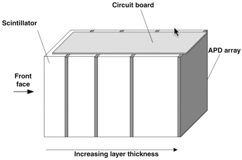
A DOI design using layers of crystal slabs. APD arrays are used to read out light from each layer. The light distribution in each slab is used to determine the point of interaction in each slab. The layers are also useful in handling events that scatter within the detector module.
Another approach is to use single- or double-ended readout designs of thick crystal slabs and extract the DOI information from the changes in the measured LRFs (Hunter et al 2007, Ling et al 2007, Moore et al 2007). The double-ended approach is essentially the same as used for the double-ended DOI scheme for discrete crystals. One or both of the two photosensors (in this case, arrays or position-sensitive devices) are used to determine the event position centroid as projected on the surface of the detector, and the ratio of the signals between the two arrays is used to determine the DOI. However, one can also derive DOI information from a single-ended readout of a thick crystal slab (Moore et al 2007, Ling et al 2007, Lerche et al 2005) with appropriate modeling of the shape of the LRF as a function of depth. Figure 22 shows one such device being developed for a pre-clinical PET scanner. Currently, the module uses a 50 × 50 × 8 mm3 crystal coupled to a 64-anode PMT to provide <1.4 mm spatial resolution and 1 bit of DOI data. As the technology is improved, one can expect to see much thicker crystals (15–25 mm thick) with improved DOI resolution as well. In both of these approaches, the continued development of fast, bright scintillators is important. Since measurement of the LRF shape is needed, a bright scintillator is needed to reduce the noise of the measured shape (improves the accuracy of the estimation). At the same time, fast scintillators reduce the light pile-up that can distort the LRF shapes with a count rate if the detector needs to handle high single rates. While there have been various approaches to correcting the integrated pulse data from pile-up effects, most PET scanners have not implemented sophisticated pile-up correction schemes. In the future, we are likely to see such schemes used to further reduce variance in LRF shapes for detector designs with statistical position estimators such as those being used in these DOI approaches. One disadvantage of the thick slab approach (as compared to the layered slab designs) is that there is less information from the detector about events that scatter within the detector. Thus, scatter for the thick slab designs must be incorporated in the estimation technique. At the same time, the thick slab approach has the advantage of providing a continuous DOI readout that can be improved as scintillators become brighter. The thick slab designs also have the advantage of requiring fewer electronic channels.
Figure 22.
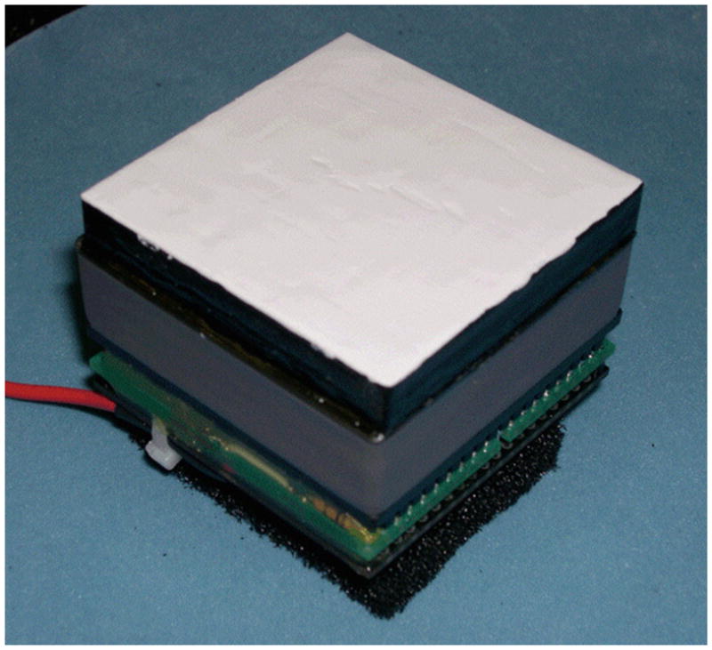
An example of an assembled ‘thick’ slab detector. A 50 × 50 × 8 mm3 LYSO crystal is mounted on a 64-anode PMT. A statistical estimation approach is used to provide a spatial resolution of ~1.4 mm and at least 2 bits of DOI information. Several investigators are working to use thicker slabs and improve both the spatial resolution and DOI capabilities of such designs.
Alternate designs
While scintillator-based detector designs still dominate scanner designs, there has always been interest in alternative approaches—generally with the goal of being able to offer much higher spatial resolution with higher packing fractions. Of course, the hope is always that such goals can be accomplished at a lower cost than very high volume resolution (<1 mm3) scintillator-based designs. Some of the earliest such alternatives were based on wire chambers, and one such design has been commercialized for pre-clinical applications and at least one research system has been used for human studies (Ott 1993, Schafers et al 2005). These devices have included chambers with converter foils as well as photosensitive chambers that view scintillators. While there is still ongoing work with wire chambers, most efforts recently on non-scintillator solutions have been focused elsewhere. In a similar fashion, there have been several efforts to utilize plastic scintillator sheets or layers of scintillation fibers as high spatial resolution detectors. Due to the lack of good photoelectric cross section in these types of detectors, they have not made an impact on human whole-body imaging (lack of sensitivity and scatter rejection) compared to the many other solutions. However, much as wire chambers, these devices are being considered for pre-clinical imaging and a small animal system based on layers of fiber optic scintillation detectors has been built (Tsyganov et al 2006). Another area that is being looked at again is the use of liquid xenon as a scintillator, in particular for TOF PET (Doke et al 2006, Gallin-Martel et al 2006). One of the principal advantages of layered fiber or wire chamber designs is that the multiple interactions within the detector system can be kept essentially independent, making the estimation of the point of first interaction a simpler task. Another variation on this concept is that of the resistive plate chamber (a gaseous particle detector: RPC). At least, one group investigates RPC devices for small animal PET (Blanco et al 2006), and there have been discussions about investigating such technology for human whole-body scanners. Prototype devices have obtained spatial resolutions of 0.5 mm with timing resolutions of ~300 ps. A drawback of these devices is that they do not provide energy resolution, raising concerns about high-scattered event rates and the impact on single rates (randoms). However, all of these systems are generally more complex to fabricate into a scanner than scintillator or solid-state-based solutions. This leads us to consider some of the solid-state solutions being investigated.
One area of development is that of silicon detectors. One challenge in considering silicon detectors is that such devices have a relatively low proton number compared to scintillators commonly used in PET designs. For example, if one compares a 4.8 cm thick Si detector to a 1 cm thick BGO detector, the probability of interactions for Si is ~48% and for BGO ~58%, but the photofraction for Si is <1% compared to ~43% for BGO (Cesca et al 2007). However, silicon detectors generate a large number of charge carriers per unit of energy absorbed and these carriers have good mobility. As a result, these devices generally have very good energy resolution. With a prototype silicon pad detector, Park et al (2007a, 2007c) have obtained ~1% energy resolution for 140.5 keV and a 82 ns timing resolution for 511 keV events. The detector used for this experiment is intended for use as a Compton scatter detector since more than 99% of the first interactions will be Compton at 511 keV. In such a design, the silicon detector is placed in front of a more conventional PET detector array (e.g. BGO or LSO blocks). Those events that interact in the pad detector (and are then absorbed in the conventional PET detector ring) will provide the highest spatial resolution with good sensitivity. For the design presented by Park et al, the simulations for a small animal system indicate spatial resolutions of ~1 mm with a 9% sensitivity (for those events that interact in the pad detector) and about 1.7 mm resolution with a 21% sensitivity for a ring of 3 × 3 × 20 mm3 BGO detectors as the conventional PET detector portion of the system. The prototypes in this work were originally developed for Compton imaging and consisted of detectors with 1.4 mm2 pads arranged in a 32 × 16 array (512 pads). Thus, each detector has 512 channels and this means that a very large number of electronics channels will need to be accommodated for such a system. Since silicon detectors are also of interest in high energy physics, there are ASICs available for reading out such systems. However, if timing resolutions of 82 ns such as were obtained by Park et al are normal for such devices, their application will be restricted to relatively low count rate pre-clinical systems.
Another approach with silicon detectors is to implement a row/column scheme similar in concept to what has been proposed for scintillator detector systems by using silicon strip detectors rather than pad detectors (figure 23). Again, such a detector can be used in a Compton imaging arrangement as is being developed by Park et al. However, another group which focused on pre-clinical imaging has proposed stacking many layers of silicon strip detectors to form the entire detector system (Cesca et al 2007). Due to the low photoelectric fraction, the proposal is to only keep those events that occur once in the stack (discard all multiple events due to scatter within the detector stacks). Such an approach will provide very high spatial resolution, but has not been adopted by a large number of PET detector developers due to the low photofraction and the resulting sensitivity issues when using silicon devices. An alternative that has received increasing attention is the use of CdZnTe (CZT) and CdTe room temperature semiconductors that have been under development for a number of years.
Figure 23.

An example of a silicon strip detector. The gamma ray produces hole–electron pairs that are collected on the strips and the charge then directed to appropriate amplifiers. On the right is an example of one such detector used at the University of Arizona.
CZT and CdTe can be made into large detectors with either pixelated anodes or cross strip anodes for reading out resolution elements. One of the main differences between the two materials is the charge transport properties. The actual differences can favor either CZT or CdTe depending on the growth techniques used and the temperature of the devices. Most investigators have reported that the charge mobility of CdTe is somewhat better (typically on the order of 20%) at room temperature. The devices generally have much better energy resolution than scintillator-based detectors and can be made to provide very good spatial resolution. The challenges for PET have been timing resolution (they generally have low charge mobility) and the low photopeak detection efficiency for 511 keV gamma rays (Arnaud et al 2007, Levin et al 2006, Vaska et al 2006). CZT and CdTe detectors have not been developed for any human PET scanners due to the challenges in timing resolution. However, for pre-clinical imaging, the small size of the subjects and the restrictions on dose administered make the timing challenges of CZT/CdTe less critical. One approach for a CZT detector being developed at Stanford is illustrated in figure 24, and a similar approach has been investigated for CdTe (Hadong et al 2007). The investigators at Stanford use 40 × 40 × 5 mm3 slabs of CZT to provide sufficient stopping power and maintain good spatial resolution. In this design, orthogonal anode and cathode strips are sandwiched between the CZT slabs to provide spatial decoding. The slabs are 5 mm wide along one axis, and the orthogonal strips are used to localize the event within each slab. Such a design will have multiple interactions within the detector, so once again a mechanism to measure DOI is needed. With the orthogonal anode/cathode strips and the limited charge mobility in CZT, an event in the slab is only ‘seen’ by the local strips. Much in the same way as a pad detector, this feature of CZT allows multiple events within the slab to be recorded independently. For this design, the investigators plan to use the kinematics of Compton scattering within the detector array along with the fine pitch readout (ability to separate multiple interactions into separate events) to sort out the most likely point of the first interaction (Chinn et al 2007).
Figure 24.
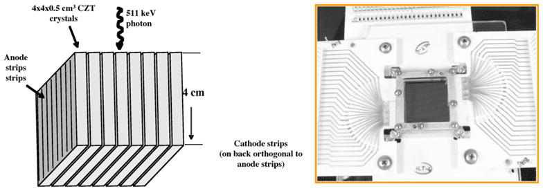
A design for a PET detector based on CZT (left) and an image of a 32 × 32 × 2 mm3 CZT prototype detector element being developed at Stanford University.
One might wonder about high purity germanium (HPGe) detectors—long a mainstay of high resolution x-ray and gamma-ray spectroscopy. As with CdTe and CZT, advances have been made in growing HPGe detectors and the fabrication of HPGe strip detectors is available from commercial suppliers. With the use of orthogonal strips, these detectors can perform DOI determination much as is done with the CdTe and CZT approaches we have already mentioned and there is a project exploring such detectors for use in PET (Cooper et al 2007a, 2007b). In addition, HPGe offers very high energy resolution (better than CZT), useful in determining the point of first interaction both within the detector and in rejected events that scatter in the object being scanned. HPGe is a mature technology and is available in much larger volumes than other materials used in solid-state detectors. HPGe detectors are probably limited to pre-clinical applications due to the timing resolution of HPGe detectors and the complications of keeping the detectors cold enough.
The ongoing challenge of detector design
While this review has presented more material on scintillator designs than on alternative approaches (e.g. solid state detectors, wire chambers, etc), the basic challenges for all design directions are similar. With the increasing use of PET/CT scanners in the clinic and PET and PET/CT scanners for pre-clinical imaging and the preliminary developments in MRI/PET systems, there is ample incentive for instrument designers to continue to push the capabilities of detector systems to attack the goals of improved spatial resolution, improved sensitivity and improved timing. In the beginning, we listed the main attributes for a PET detector. As we have seen, there is no one solution. But it is even more complex than we have discussed thus far. As we push the limits of the detectors, we cannot do so without considering other aspects of the potential scanner system, in particular the image reconstruction algorithm. With the everincreasing computing power available and the continued advancement in statistical image reconstruction algorithms that can include the physical effects of the photon transport in both the object and the detector system, it is not always clear where to put the most development effort in the basic detector. For example, DOI can be done at the detector level based on single events, or the basic distribution of data in the detector array can be passed directly to the reconstruction engine and it can use coincidence information to provide more information on the limits of the direction of the incident gamma rays to aid in the point of first interaction determination within the detector array. Thus, modern detector designers really have to start looking at potential system architectures and image reconstruction capabilities early on their efforts.
Another aspect is to keep track of what is feasible in support electronics. We mentioned this point earlier, but is worth mentioning again. If one believes that the best way to obtain optimal performance is to keep all of the event information you can and use it in the final image formation process, then the electronics are going to need to process and transfer large amounts of data. For years, PET system designers have worked to reduce the number of data channels (many-on-one crystal to photoreceptor coupling, multiplexing data, etc). But with the rapid improvements in FPGAs and similar field programmable devices, high-speed serial ADCs and the ability to make very compact assemblies, it is now possible to rethink how much data can be collected and processed. The challenges of such high density systems are significant (e.g. heat generation, number of interconnects, expense of production), but ever more feasible and we can already see new designs that increase the number of data channels significantly.
During the preparation of this review, I was asked to summarize what the most promising technologies are and where the field is going (and what does it really need). My ‘crystal ball’ is certainly not infallible and my comments along these lines reflect my own personal views (and experience) and are always subject to change as clever individuals find ways to make various technologies more attractive and practical than one might expect. Let us start with the question of what the field needs. The answer depends on the task. As I noted in the beginning, I like to divide PET systems into three main categories: (1) pre-clinical, (2) dedicated neuro-imaging (or other specialized small area imaging applications like breast scanners) and (3) whole-body scanning. For pre-clinical, I feel that the spatial resolution target should be 700 μm in order to provide whole-body mouse imaging with about the same volume resolution as we currently obtain in human body scans (based on simple scaling of the body mass). Thus, pre-clinical detector systems need to push the resolution envelope. One of the big problems with this target is also getting enough sensitivity to achieve that resolution, and this will require DOI systems with long crystals. On the other end of the spectrum is human body imaging. There we already cannot use the limiting spatial resolution of existing scanners due to limitations in sensitivity and the amount of activity we can give the patient. Here, methods to improve the image SNR are needed and the route toward that goal is, I believe, a combination of TOF technology and ever-improved modeling of the imaging system in iterative image reconstruction algorithms. Pushing for higher spatial resolution detectors is not a major concern with our current limitations in body imaging (e.g. limited in image resolution due to the variance in the data—the need for greater sensitivity). The middle ground is neuro-imaging and other specialized imaging systems. Such devices are typically developed to provide better spatial resolution than whole-body scanners, and thus they need both better spatial resolution detectors and better sensitivity. The sensitivity improvements are achieved, in part, by using smaller detector ‘rings’ (more solid angle) and thus DOI technology is needed to compensate for the parallax errors seen in small ring geometries. Thus, we really seem to be focused on two major areas—TOF and DOI—as key technologies for the future. What is preventing these technologies from going forward? TOF is already a commercial reality, but the TOF resolution needs to be improved to provide a greater impact on the image quality. The challenges here are finding cost-effective solutions for fast scintillators and fast photosensors. The electronics is not as great an issue other than finding ways to provide reliable fast timing at affordable cost points. With the exception of a small animal imaging system from GE and a limited production-dedicated neuro-scanner from Siemens, the various DOI solutions have not made their way into full commercial production scanners. Again, the problems are cost-effective solutions that clearly offer better performance than ‘simply’ modeling the detector response in the image reconstruction software. Major changes in system designs are slow to occur in commercial scanners due to the costs involved, and most systems are evolutions of the previous models. Of course, if new technologies can be implemented as a relatively modest incremental design change in a scanner, they may be commercialized even if the impact is primarily for marketing purposes. Thus, for major development of a new technology (be it DOI or TOF or both or something I have not mentioned), the change should provide dramatic improvements in performance and be cost effective to produce in order for a vendor to justify the engineering and product development expense. For example, in DOI designs, approaches that can use single-ended readout schemes result in less photosensors and smaller numbers of electronic channels which make them more cost effective than other approaches. Further, designs using slabs of scintillators rather than discrete crystals also provide cost savings.
The trends are clear—both in universities and in commercial vendor laboratories—and that is improvements in TOF and DOI solutions coupled with improved modeling of the scanner system and photon transport in the reconstruction software. What are the most promising technologies? Here I am very biased toward scintillator-based solutions. With the potential of SiPMs to provide cost-effective, high performance photosensors (in both quantum efficiency and timing), scintillator-based designs can be compact, offer high packing fractions and implement several different designs for DOI. Solid-state detectors are of considerable interest, but so far they have not offered dramatically better performance for PET applications, have challenges in terms of stopping power for 511 keV photons and are generally more costly than scintillator-based approaches. One area where solid-state detectors can offer performance superior to scintillator-based systems is that of energy resolution. While the very high energy resolution of materials such as HPGe offers far better rejection of gamma rays that scatter in the object being imaged, the success of model-based scatter corrections in current PET scanner systems makes this advantage less critical than one might first imagine. Given the needs of PET systems to provide high spatial resolution, fast timing and high sensitivity, I feel that scintillators will continue to dominate scanner designs. Further, my crystal ball predicts that the winner for the ultimate detector design is likely to be a mosaic detector made up of elements consisting of slabs of crystal (perhaps 50 × 50 mm2) viewed by arrays of SiPMs and supported by statical-based estimation algorithms that locate events in the crystal slabs in three dimensions.
As we have seen, PET detector development is a very active area of investigation around the world. It ranges from incremental improvements on existing designs to radically different approaches and materials. While the ideal detector has yet to be realized, the capabilities of modern scanners have continued to advance as the improved designs have gone into commercial production or been assembled into full scanners at various research laboratories.
Acknowledgments
I would like to thank all the members of the Nuclear Medicine Physics Group at the University of Washington for making it possible for me to find the time to write this article—and for their insight and good work that has allowed our laboratory to work on detector and scanner development so consistently over the years. In particular, I wish to thank Robert Miyaoka for his fine work on the MiCES detectors, Larry MacDonald, Wendy McDougald, and Catherine Lockhart for their work on our DOI and MR detector projects as well as Robert Harrison for development of the simulation tools we use routinely in our work. I also am happy to acknowledge the patience and skills of Paul Kinahan and Adam Alessio in working with me on so many image reconstruction and data analysis tasks—in particular those dealing with modeling detector response in the image reconstruction algorithm. If space permitted, I would also list all of those investigators that have done so much for the field and have taken the time to assist my laboratory and myself over the years. Last, but far from least, I wish to thank the National Cancer Institute, the National Institute for Biomedical Imaging and Bioengineering, as well as General Electric Medical Systems, Philips Medical Systems, Siemens Medical Systems, Zecotek Photonics, and Altera corporation for their generous support of our laboratory.
References
- Alessio AM, Kinahan PE, Lewellen TK. Modeling and incorporation of system response functions in 3D whole body PET. 2004 IEEE Nucl. Sci. Symp. Conf. Record (IEEE Cat Cat. No. 04CH37604); 2004. pp. 3992–6. [Google Scholar]
- Amaral P, Carrico B, Ferreira M, Moura R, Ortigao C, Rodrigues P, Da Silva JC, Trindade A, Varela J. Performance and quality control of clear-PEM detector modules. Nucl Instrum Methods Phys Res. 2007;A 580:1123–6. [Google Scholar]
- Drezet A, Monnet O, Mathy F, Montemont G, Loick V. CdZnTe detectors for small field of view positron emission tomographic imaging. Nucl Instrum Methods Phys Res. 2007;A 571:465–70. [Google Scholar]
- Barrett HH, Myers KJ. Foundations of Image Science. Hoboken, NJ: Wiley; 2004. p. 1540. [Google Scholar]
- Bauer F, Loope M, Schmand M, Eriksson L. Evaluation of a micro-channel plate PMT in PET. 2006 IEEE Nucl. Sci. Symp. Conf. Record (IEEE Cat Cat. No. 06CH37832); 2007. pp. 2503–5. [Google Scholar]
- Blanco A, Carolino N, Correia CMBA, Fazendeiro L, Ferreira NC, Marques MFF, Marques RF, Fonte P, Gil C, Macedo MP. RPC-PET: a new very high resolution PET technology. IEEE Trans Nucl Sci. 2006;53:2489–94. [Google Scholar]
- Boston HC, et al. Characterization of the smartPET planar germanium detectors. Nucl Instrum Methods Phys Res. 2007;A 579:104–7. [Google Scholar]
- Braem A, Chesi E, Ciocia F, De Leo R, Joram C, Lagamba L, Nappi E, Seguinot J, Vilardi I, Weilhammer P. Scintillator studies for the HPD-PET concept. Nucl Instrum Methods Phys Res. 2007a;A 571:419–24. [Google Scholar]
- Braem A, Chesi E, Joram C, Seguinot J, Weilhammer P, De Leo R, Nappi E, Lustermann W, Schinzel D, Johnson I, Renker D, Albrecht S. High precision axial coordinate readout for an axial 3-D PET detector module using a wave length shifter strip matrix. Nucl Instrum Methods Phys Res. 2007b;A 580:1513–21. [Google Scholar]
- Britvitch I, Deiters K, Ingram Q, Kuznetsov A, Musienko Y, Renker D, Reucroft S, Sakhelashvili T, Swain J. Avalanche photodiodes now and possible developments. Nucl Instrum Methods Phys Res. 2004;A 535:523–7. [Google Scholar]
- Britvitch I, Johnson I, Renker D, Stoykov A, Lorenz E. Characterization of Geiger-mode avalanche photodiodes for medical imaging applications. Nucl Instrum Methods Phys Res. 2007;A 571:308–11. [Google Scholar]
- Bruyndonckx P, Lemaitre C, Schaart D, Maas M, van der Laan DJ, Krieguer M, Devroede O, Tavernier S. Towards a continuous crystal APD-based PET detector design. Nucl Instrum Methods Phys Res. 2007;A 571:182–6. [Google Scholar]
- Budinger TF. PET instrumentation: what are the limits? Semin Nucl Med. 1998;28:247–67. doi: 10.1016/s0001-2998(98)80030-5. [DOI] [PubMed] [Google Scholar]
- Burr KC, Ivan A, Castleberry DE, Thompson RA, LeBlanc JW, Shah KS, Farrell R. Depth-of-interaction-encoding high-resolution PET detector with sub-nanosecond timing. 2004 IEEE Nucl. Sci. Symp. Conf. Record (IEEE Cat. No. 04CH37604); 2004a. pp. 3880–4. [Google Scholar]
- Burr KC, Ivan A, Castleberry DE, Thompson RA, LeBlanc JW, Shah KS, Farrell R. Evaluation of a prototype small-animal PET detector with depth-of-interaction encoding. IEEE Trans Nucl Sci. 2004b;51:1791–8. [Google Scholar]
- Casey M, Nutt R. A multicrystal two dimensional BGO detector system for positron emission tomography. IEEE Trans Nucl Sci. 1986;33:460–3. [Google Scholar]
- Catana C, Wu Y, Judenhofer MS, Qi J, Pichler BJ, Cherry SR. Simultaneous acquisition of multislice PET and MR images: initial results with a MR-compatible PET scanner. J Nucl Med. 2006;47:1968–76. [PubMed] [Google Scholar]
- Cesca N, Auricchio N, Di Domenico G, Zavattini G, Malaguti R, Andritschke R, Kanbach G, Schopper F. SiliPET: design of an ultra-high resolution small animal PET scanner based on stacks of semi-conductor detectors. Nucl Instrum Methods Phys Res. 2007;A 572:225–7. [Google Scholar]
- Chatziioannou A, Tai YC, Doshi N, Cherry SR. Detector development for microPET II: a 1 microl resolution PET scanner for small animal imaging. Phys Med Biol. 2001;46:2899–910. doi: 10.1088/0031-9155/46/11/310. [DOI] [PubMed] [Google Scholar]
- Cherry SR. In vivo molecular and genomic imaging: new challenges for imaging physics. Phys Med Biol. 2004;49:R13–48. doi: 10.1088/0031-9155/49/3/r01. [DOI] [PubMed] [Google Scholar]
- Chinn G, Foudray AMK, Levin CS. A method to include single photon events in image reconstruction for a 1 mm resolution PET system built with advanced 3-D positioning detectors. 2006 IEEE Nucl. Sci. Symp. Conf. Record (IEEE Cat. No. 06CH37832); 2007. pp. 1740–5. [Google Scholar]
- Chung YH, Choi Y, Cho G, Choe YS, Lee KH, Kim BT. Characterization of dual layer phoswich detector performance for small animal PET using Monte Carlo simulation. Phys Med Biol. 2004;49:2881–90. doi: 10.1088/0031-9155/49/13/008. [DOI] [PubMed] [Google Scholar]
- Cooper RJ, et al. SmartPET: applying HPGe and pulse shape analysis to small-animal PET. Nucl Instrum Methods Phys Res. 2007a;A 579:313–7. [Google Scholar]
- Cooper RJ, et al. Position sensitivity of the first SmartPET HPGe detector. Nucl Instrum Methods Phys Res. 2007b;A 573:72–5. [Google Scholar]
- Costa E, Massaro E, Piro L. A BGO-CsI(TI) phoswich: a new detector for x-and y-ray astronomy. Nucl Instrum Methods Phys Res. 1986;A 243:572–7. [Google Scholar]
- Couceiro M, Blanco A, Ferreira Nuno C, Ferreira Marques R, Fonte P, Lope L. RPC-PET: status and perspectives. Nucl Instrum Methods Phys Res. 2007;A 580:915–8. [Google Scholar]
- Croci G, Ropelewski L, Sauli F, Solevi P. Depth of interaction determination in GEM-based multi-layer PET detectors. Nucl Instrum Methods Phys Res. 2007;A 582:693–5. [Google Scholar]
- D’Ambrosio C, Anulli F, Bencivenni G, Domenici D, Felici G, Morone MC, Murtas F. A Hybrid parallel plate gas counter for medical imaging. Nucl Instrum Methods Phys Res. 2007;A 572:244–5. [Google Scholar]
- Dahlbom M, MacDonald LR, Eriksson L, Paulus M, Andreaco M, Casey ME, Moyers C. Performance of a YSO/LSO phoswich detector for use in a PET/SPECT system. IEEE Trans Nucl Sci. 1997;44:1114–9. [Google Scholar]
- Degenhardt C, Fiedler K, Frach T, Rutten W, Solf T, Thon A. Impact of intercrystal crosstalk on depth-of-interaction information in PET detectors. IEEE Trans Nucl Sci. 2007;54:427–32. [Google Scholar]
- Derenzo Stephen E. Mathematical removal of positron range blurring in high resolution tomography. IEEE Trans Nucl Sci. 1986;33:565–9. [Google Scholar]
- Di Domenico G, Zavattini G, Cesca N, Auricchio N, Andritschke R, Schopper F, Kanbach G. SiliPET: an ultra-high resolution design of a small animal PET scanner based on stacks of double-sided silicon strip detector. Nucl Instrum Methods Phys Res. 2007;A 571:22–5. [Google Scholar]
- Doke T, Kikuchi J, Nishikido F. Time-of-flight positron emission tomography using liquid xenon scintillation. Nucl Instrum Methods Phys Res. 2006;A 569:863–71. [Google Scholar]
- Dolgoshein B, et al. Large area silicon photomultipliers: performance and applications. Nucl Instrum Methods Phys Res. 2006;A 567:78–82. [Google Scholar]
- Du H, Yang Y, Cherry SR. Measurements of wavelength shifting (WLS) fiber readout for a highly multiplexed, depth-encoding PET detector. Phys Med Biol. 2007;52:2499–514. doi: 10.1088/0031-9155/52/9/011. [DOI] [PubMed] [Google Scholar]
- Eriksson L, Melcher CL, Eriksson M, Grazioso R, Aykac M. Design considerations for phoswich detectors for high resolution positron emission tomography. 2006 IEEE Nucl. Sci. Symp. Conf. Record (IEEE Cat. No. 06CH37832); 2007. pp. 2607–10. [Google Scholar]
- Foudray AMK, Farrell R, Olcott PD, Shah KS, Levin CS. Characterization of two thin position-sensitive avalanche photodiodes on a single flex circuit for use in 3-D positioning PET detectors. 2006 IEEE Nucl. Sci. Symp. Conf. Record (IEEE Cat. No. 06CH37832); 2007. pp. 2469–72. [Google Scholar]
- Frach T, Ruetten W, Fiedler K, Maehlum G, Solf T, Thon A. Assessment of photodiodes as a light detector for PET scanners. 2004 IEEE Nucl. Sci. Symp. Conf. Record (IEEE Cat. No. 04CH37604); 2004. pp. 4177–81. [Google Scholar]
- Gallin-Martel ML, et al. Experimental study of a liquid xenon PET prototype module. Nucl Instrum Methods Phys Res. 2006;A 563:225–8. [Google Scholar]
- Garibaldi F, et al. A PET scanner employing CsI films as photocathode. Nucl Instrum Methods Phys Res. 2004;A 525:263–7. [Google Scholar]
- Glodo J, Kuhn A, Higgins WM, van Loef EVD, Karp JS, Moses WW, Derenzo SE, Shah KS. CeBr3 for time-of-flight PET. 2006 IEEE Nucl. Sci. Symp. Conf. Record (IEEE Cat. No. 06CH37832); 2007. pp. 1570–3. [Google Scholar]
- Grignon C, et al. Simulation of a high performance gamma-camera concept for PET based on liquid xenon and gaseous photomultiplier. 2005 IEEE Int. Conf. Dielectric Liquids (IEEE Cat. No. 05CH37643); 2005. pp. 357–60. [Google Scholar]
- Guerra P, Kontaxakis G, Visvikis D, Santos A, Darambara DG. Detailed modelling of pixellated CdZnTe detectors for an accurate performance characterization of a multi-modality imaging system. 2006 IEEE Nucl. Sci. Symp. Conf. Record (IEEE Cat. No. 06CH37832); 2007. pp. 2976–9. [Google Scholar]
- Habte F, Olcott PD, Levin CS, Foudray AMK. Investigation of scintillation light multiplexing for PET detectors based on position sensitive avalanche photodiodes. 2005 IEEE Nucl. Sci. Symp. Conf. Record (IEEE Cat. No. 05CH37692C); 2006. pp. 2027–30. [Google Scholar]
- Hadong K, Cirignano L, Dokhale P, Bennett P, Stickel JR, Mitchell GS, Cherry SR, Squillante M, Shah K. CdTe orthogonal strip detector for small animal PET. 2006 IEEE Nucl. Sci. Symp. Conf. Record (IEEE Cat. No. 06CH37832); 2007. pp. 3827–30. [Google Scholar]
- Hamamoto M, Inadama N, Murayama H, Yamaya T, Tsuda T, Ono Y. DOI detection capability of 3D crystal array standing over two PMTs. 2005 IEEE Nucl. Sci. Symp. Conf. Record (IEEE Cat. No. 05CH37692C); 2006. pp. 1568–72. [Google Scholar]
- Hasegawa T, Ishikawa M, Maruyama K, Inadama N, Yoshida E, Murayama H. Depth-of-interaction recognition using optical filters for nuclear medicine imaging. 2003 IEEE Nucl. Sci. Symp. Conf. Record (IEEE Cat. No. 03CH37515); 2004. pp. 2164–8. [Google Scholar]
- Hasegawa T, et al. Evaluation of static physics performance of the jPET-D4 by Monte Carlo simulations. Phys Med Biol. 2007;52:213–30. doi: 10.1088/0031-9155/52/1/014. [DOI] [PubMed] [Google Scholar]
- Herbert DJ, Moehrs S, D’Ascenzo N, Belcari N, Del Guerra A, Morsani F, Saveliev V. The silicon photomultiplier for application to high-resolution positron emission tomography. Nucl Instrum Methods Phys Res. 2007;A 573:84–7. [Google Scholar]
- Hunter WCJ, Barrett HH, Furenlid LR, Moore SK. Method of calibrating response statistics for ML estimation of 3D interaction position in a thick-detector gamma camera. IEEE Nucl. Sci. Symp. Conf. Record NSS ‘07; 2007. pp. 4359–63. [DOI] [PMC free article] [PubMed] [Google Scholar]
- Imrek J, et al. Development of an improved detector module for miniPET-II. 2006 IEEE Nucl. Sci. Symp. Conf. Record (IEEE Cat. No. 06CH37832); 2007. pp. 3037–40. [Google Scholar]
- Inadama N, Murayama H, Tsuda T, Nishikido F, Shibuya K, Yamaya T, Yoshida E, Takahashi K, Ohmura A. Optimization of crystal arrangement on 8-layer DOI PET detector. 2006 IEEE Nucl. Sci. Symp. Conf. Record (IEEE Cat. No. 06CH37832); 2007. pp. 3082–5. [Google Scholar]
- Inadama N, Murayama H, Yamaya T, Kitamura K, Yamashita T, Kawai H, Tsuda T, Sato M, Ono Y, Hamamoto M. BGO DOI-detector composed of three-dimensional crystal array for PET. 2004 IEEE Nucl. Sci. Symp. Conf. Record (IEEE Cat. No. 04CH37604); 2004. pp. 2729–33. [Google Scholar]
- Ishii K, et al. First achievement of less than 1 mm FWHM resolution in practical semiconductor animal PET scanner. Nucl Instrum Methods Phys Res. 2007;A 576:435–40. [Google Scholar]
- Jakoby BW, Bercier Y, Watson CC, Rappoport V, Young J, Bendriem B, Townsend DW. Physical performance and clinical workflow of a new LSO HI-REZ PET/CT scanner. 2006 IEEE Nucl. Sci. Symp. Conf. Record (IEEE Cat. No. 06CH37832); 2007. pp. 3130–4. [Google Scholar]
- Joung J, Miyaoka RS, Kohlmyer SG, Lewellen TK. Implementation of ML based positioning algorithms for scintillation cameras. IEEE Trans Nucl Sci. 2000;47:1104–11. [Google Scholar]
- Joung J, Miyaoka RS, Lewellen TK. cMiCE: a high resolution animal PET using continuous LSO with a statistics based positioning scheme. Nucl Instrum Methods. 2002;A 459:584–98. [Google Scholar]
- Judenhofer MS, Catana C, Swann BK, Siegel SB, Jung WI, Nutt RE, Cherry SR, Claussen CD, Pichler BJ. PET/MR images acquired with a compact MR-compatible PET detector in a 7-T magnet. Radiology. 2007;244:807–14. doi: 10.1148/radiol.2443061756. [DOI] [PubMed] [Google Scholar]
- Junichi O, Hiromichi T. Investigation of a whole-body DOI-PET system. Nucl Instrum Methods Phys Res. 2007;A 571:223–6. [Google Scholar]
- Karakash A, et al. Timing by silicon photomultiplier: a possible application for TOF measurements. Nucl Instrum Methods Phys Res. 2006;A 567:353–5. [Google Scholar]
- Karp JS, Muehllehner G, Mankoff DA, Ordonez CE, Ollinger JM, Daube-Witherspoon ME, Haigh AT, Beerbohm DJ. Continuous-slice PENN-PET: a positron tomograph with volume imaging capability. J Nucl Med. 1990;31:617–27. [PubMed] [Google Scholar]
- Karp JS, Surti S, Daube-Witherspoon ME, Freifelder R, Cardi CA, Adam LE, Bilger K, Muehllehner G. Performance of a brain PET camera based on Anger-logic gadolinium oxyorthosilicate detectors. J Nucl Med. 2003;44:1340–9. [PubMed] [Google Scholar]
- Kikuchi Y, Ishii K, Yamazaki H, Matsuyama S, Momose G, Ishizaki A, Kisaka J, Kudo T. Feasibility of ultra high resolution better than 1 mm FWHM of small animal PET by using CdTe detector arrays. 2006 IEEE Nucl. Sci. Symp. Conf. Record (IEEE Cat. No. 06CH37832); 2007. pp. 2454–7. [Google Scholar]
- Kim CL. A study on the temperature characteristics of LYSO PET detector. 2005 IEEE Nucl. Sci. Symp. Conf. Record (IEEE Cat. No. 05CH37692C); 2006. pp. 2013–6. [Google Scholar]
- Kuhn A, Surti S, Karp JS, Muehllehner G, Newcomer FM, VanBerg R. Performance assessment of pixelated LaBr3 detector modules for time-of-flight PET. IEEE Trans Nucl Sci. 2006;53:1090–5. [Google Scholar]
- LeBlanc JW, Thompson RA. A novel PET detector block with three dimensional hit position encoding. 2003 IEEE Nucl. Sci. Symp. Conf. Record (IEEE Cat. No. 03CH37515); 2004. pp. 1718–22. [Google Scholar]
- Lee K, Kinahan PE, Fessler JA, Miyaoka RS, Janes M, Lewellen TK. Pragmatic fully 3D image reconstruction for the MiCES mouse imaging PET scanner. Phys Med Biol. 2004;49:4563–78. doi: 10.1088/0031-9155/49/19/008. [DOI] [PubMed] [Google Scholar]
- Lerche CW, et al. Depth of gamma-ray interaction within continuous crystals from the width of its scintillation light-distribution. IEEE Trans Nucl Sci. 2005;52:560–72. [Google Scholar]
- Levin CS, Foudray AM, Habte F. Impact of high energy resolution detectors on the performance of a PET system dedicated to breast cancer imaging. Phys Med Biol. 2006;21:28–34. doi: 10.1016/S1120-1797(06)80020-7. [DOI] [PubMed] [Google Scholar]
- Lewellen TK. Time-of-flight PET. Semin Nucl Med. 1998;28:268–75. doi: 10.1016/s0001-2998(98)80031-7. [DOI] [PubMed] [Google Scholar]
- Lewellen TK, Janes M, Miyaoka RS. DMice—a depth-of-interaction detector design for PET scanners. 2003 IEEE Nucl. Sci. Symp. Conf. Record (IEEE Cat. No. 03CH37515); 2004. pp. 2388–92. [DOI] [PMC free article] [PubMed] [Google Scholar]
- Lewellen TK, Karp J. Basic PET principles. In: Wenick MN, Aarsvold JN, editors. Emission Tomography: The Fundamentals of PET and SPECT. New York: Academic; 2004. [Google Scholar]
- Ling T, Lewellen TK, Miyaoka RS. Depth of interaction decoding of a continuous crystal detector module. Phys Med Biol. 2007;52:2213–28. doi: 10.1088/0031-9155/52/8/012. [DOI] [PubMed] [Google Scholar]
- Liu H, Zhao Q, Shi P. Performance results of BGO block detectors based on flat panel PS-PMT for PET. IEEE Trans Nucl Sci. 2007;54:1298–301. [Google Scholar]
- Lucas AJ, Hawkes RC, Ansorge RE, Williams GB, Nutt RE, Clark JC, Fryer TD, Carpenter TA. Development of a combined microPET-MR system. Technol Cancer Res Treat. 2006;5:337–41. doi: 10.1177/153303460600500405. [DOI] [PubMed] [Google Scholar]
- Mackewn J, Strul D, Hallett WA, Halsted P, Page RA, Keevil SF, Williams SCR, Cherry SR, Marsden PK. Design and development of an MR-compatible PET scanner for imaging small animals. 2004 IEEE Nucl. Sci. Symp. Conf. Record (IEEE Cat. No. 04CH37604); 2004. pp. 3271–4. [Google Scholar]
- Mackewn JE, Keevil SF, Hallett WA, Halsted P, Page RA, Kelly M, Williams SCR, Marsden PK. An MR compatible LSO-PET scanner for molecular imaging studies. 2006 IEEE Nucl. Sci. Symp. Conf. Record (IEEE Cat. No. 06CH37832); 2007. pp. 2986–9. [Google Scholar]
- Mateo F, Aliaga RJ, Martinez JD, Monzo JM, Gadea R. Incidence position estimation in a PET detector using a discretized positioning circuit and neural networks. Computational and Ambient Intelligence—Proc. 9th Int. Work Conf. on Artificial Neural Networks, IWANN 2007; 2007. pp. 684–91. [Google Scholar]
- McCallum S, Clowes P, Welch A. A four-layer attenuation compensated PET detector based on APD arrays without discrete crystal elements. Phys Med Biol. 2005;50:4187–207. doi: 10.1088/0031-9155/50/17/019. [DOI] [PubMed] [Google Scholar]
- McClish M, Dokhale P, Christian J, Stapels C, Shah KS. Characterization and scintillation studies of a solid-state photomultiplier. Nucl Instrum Methods Phys Res. 2007;A 572:1065–70. doi: 10.1016/j.nima.2010.03.004. [DOI] [PMC free article] [PubMed] [Google Scholar]
- McElroy DP, Pimpl W, Djelassi M, Pichler BJ, Rafecas M, Schuler T, Ziegler SI. First results from MADPET-II: a novel detector and readout system for high resolution small animal PET. 2003 IEEE Nucl. Sci. Symp. Conf. Record (IEEE Cat. No. 03CH37515); 2004. pp. 2043–7. [Google Scholar]
- McElroy DP, Saveliev V, Reznik A, Rowlands LA. Evaluation of silicon photomultipliers: a promising new detector for MR compatible PET. Nucl Instrum Methods Phys Res. 2007;A 571:106–9. [Google Scholar]
- Milster TD, Selberg LA, Barrett HH, Landesman AL, Seacat RH. Digital position estimation for the modular scintillation camera. IEEE Trans Nucl Sci. 1985;N532(1):748–52. [Google Scholar]
- Miyaoka R, Lewellen TK, Yu H. Design of a depth of interaction (DOI) PET detector module. IEEE Nuclear Science Symp. and Medical Imaging Conf.; 1997. pp. 939–43. [Google Scholar]
- Miyaoka RS, Janes ML, Lee K, Park B, Kinahan PE, Lewellen TK. Development of a single detector ring micro crystal element scanner: quickPET II. Mol Imaging. 2005;4:117–27. doi: 10.1162/15353500200504154. [DOI] [PubMed] [Google Scholar]
- Moehrs S, Del Guerra A, Herbert DJ, Mandelkern MA. A detector head design for small-animal PET with silicon photomultipliers (SiPM) Phys Med Biol. 2006;51:1113–27. doi: 10.1088/0031-9155/51/5/004. [DOI] [PubMed] [Google Scholar]
- Moore SK, Hunter WCJ, Furenlid LR, Barrett HH. Maximum-likelihood estimation of 3D event position in monolithic scintillation crystals: experimental results. 2007 IEEE Nucl. Sci. Symp. Conf. Record; 2007. pp. 3691–4. [DOI] [PMC free article] [PubMed] [Google Scholar]
- Moses WW. Recent advances and future advances in time-of-flight PET. Nucl Instrum Methods Phys Res. 2007;A 580:919–24. doi: 10.1016/j.nima.2007.06.038. [DOI] [PMC free article] [PubMed] [Google Scholar]
- Moses WW, Derenzo SE, Nutt R, Digby WM, Williams CW, Andreaco M. Performance of a PET detector module utilizing an array of silicon photodiodes to identify the crystal of interaction. IEEE Trans Nucl Sci. 1993;40:1036–40. [Google Scholar]
- Moses WW, Shah KS. Potential for RbGd2Br7:Ce, LaBr3:Ce, LaBr3:Ce, and LuI3:Ce in nuclear medical imaging. Nucl Instrum Methods Phys Res. 2005;A 537:317–20. [Google Scholar]
- Muehllehner G, Karp JS. A positron camera using position-sensitive detectors: PENN-PET. J Nucl Med. 1986;27:90–8. [PubMed] [Google Scholar]
- Murtas F, et al. A triple GEM gamma camera for medical application. Nucl Instrum Methods Phys Res. 2007;A 572:266–7. [Google Scholar]
- Musienko Y, Auffray E, Lecoq P, Reucroft S, Swain J, Trummer J. Study of multi-pixel Geiger-mode avalanche photodiodes as a read-out for PET. Nucl Instrum Methods Phys Res. 2007;A 571:362–5. [Google Scholar]
- Nishikido F, Tsuda T, Inadama N, Yoshida E, Takahashi K, Shibuya K, Yamaya T, Kitamura K, Murayama H. Spatial resolution measured by a prototype system of two four-layer DOI detectors for jPET-RD. 2006 IEEE Nucl. Sci. Symp. Conf. Record (IEEE Cat. No. 06CH37832); 2007. pp. 3041–4. [Google Scholar]
- Ott RJ. Wire chambers revisited. Eur J Nucl Med. 1993;20:348–58. doi: 10.1007/BF00169813. [DOI] [PubMed] [Google Scholar]
- Otte AN, Barral J, Dolgoshein B, Hose J, Klemin S, Lorenz E, Mirzoyan R, Popova E, Teshima M. A test of silicon photomultipliers as readout for PET. Nucl Instrum Methods Phys Res. 2005;A 545:705–15. [Google Scholar]
- Pani R, et al. LaBr3:Ce crystal: the latest advance for scintillation cameras. Nucl Instrum Methods Phys Res. 2007;A 572:268–9. [Google Scholar]
- Park SJ, Rogers WL, Clinthorne NH. Design of a very high-resolution small animal PET scanner using a silicon scatter detector insert. Phys Med Biol. 2007a;52:4653–77. doi: 10.1088/0031-9155/52/15/019. [DOI] [PubMed] [Google Scholar]
- Park SJ, et al. A prototype of very high-resolution small animal PET scanner using silicon pad detectors. Nucl Instrum Methods Phys Res. 2007b;A 570:543–55. doi: 10.1016/j.nima.2006.10.277. [DOI] [PMC free article] [PubMed] [Google Scholar]
- Park SJ, et al. Performance evaluation of a very high resolution small animal PET imager using silicon scatter detectors. Phys Med Biol. 2007c;52:2807–26. doi: 10.1088/0031-9155/52/10/012. [DOI] [PubMed] [Google Scholar]
- Parra L, Barrett HH. List-mode likelihood: EM algorithm and image quality estimation demonstrated on 2-D PET. IEEE Trans Med Imaging. 1998;17:228–35. doi: 10.1109/42.700734. [DOI] [PMC free article] [PubMed] [Google Scholar]
- Peter J, Schulz RB, Semmler W. PET-MOT—a novel concept for simultaneous positron and optical tomography in small animals. 2005 IEEE Nucl. Sci. Symp. Conf. Record (IEEE Cat. No. 05CH37692C); 2006. pp. 1757–60. [Google Scholar]
- Pichler BJ, Judenhofer MS, Catana C, Walton JH, Kneilling M, Nutt RE, Siegel SB, Claussen CD, Cherry SR. Performance test of an LSO-APD detector in a 7-T MRI scanner for simultaneous PET/MRI. J Nucl Med. 2006;47:639–47. [PubMed] [Google Scholar]
- Qingguo X, Chien-Min K, Byrum K, Drake G, Vaniachine A, Wagner RG, Rykalin V, Chin-Tu C. Characterization of silicon photomultipliers for PET imaging. 2006 IEEE Nucl. Sci. Symp. Conf. Record (IEEE Cat. No. 06CH37832); 2007. pp. 1199–203. [Google Scholar]
- Ramirez RA, Soonseok K, Yuxuan Z, Shitao L, Baghaei H, Hongdi L, Yu W, Jiguo L, Wai-Hoi W. Ultrahigh-resolution L(Y)SO detectors using PMT-quadrant-sharing for human and animal PET cameras. 2006 IEEE Nucl. Sci. Symp. Conf. Record (IEEE Cat. No. 06CH37832); 2007. pp. 865–1869. [Google Scholar]
- Ramirez RA, Wai-Hoi W, Soonseok K, Baghaei H, Hongdi L, Yu W, Yuxuan Z, Shitao L, Jiguo L. A comparison of BGO, GSO, MLS, LGSO, LYSO and LSO scintillation materials for high-spatial-resolution animal PET detectors. 2005 IEEE Nucl. Sci. Symp. Conf. Record (IEEE Cat. No. 05CH37692C); 2006. pp. 2835–9. [Google Scholar]
- Raylman RR, Majewski S, Velan SS, Lemieux S, Kross B, Popov V, Smith MF, Weisenberger AG. Simultaneous acquisition of magnetic resonance spectroscopy (MRS) data and positron emission tomography (PET) images with a prototype MR-compatible, small animal PET imager. J Magn Reson. 2007;186:305–10. doi: 10.1016/j.jmr.2007.03.012. [DOI] [PMC free article] [PubMed] [Google Scholar]
- Renker D. New trends in photodetectors. Nucl Instrum Methods Phys Res. 2007;A 71:1–6. [Google Scholar]
- Safavi-Naeini M, Rosenfeld AB, Lerch MLF. PET detector module based on pixellated SI-LSO detector. Australas Phys Eng Sci Med. 2007;30:58–9. [Google Scholar]
- Sadygov Z, Olshevski A, Chirikov I, Zheleznykh I, Novilov A. Three advanced designs SOF micro-pixel avalanche photodiodes: their present status, maximum possibilities and limitations. Nucl Instrum Methods Phys Res. 2006;A 567:70–3. [Google Scholar]
- Schafers KP, Reader AJ, Kriens M, Knoess C, Schober O, Schafers M. Performance evaluation of the 32-module quadHIDAC small-animal PET scanner. J Nucl Med. 2005;46:996–1004. [PubMed] [Google Scholar]
- Seidel J, Vaquero JJ, Gandler WR, Green MV. Depth identification accuracy of a three layer phoswich PET detector module. IEEE Trans Nucl Sci. 1999;46:485–90. [Google Scholar]
- Shao Y, Li H, Gao K. Initial experimental studies of using solid-state photomultiplier for PET applications. Nucl Instrum Methods Phys Res. 2007;A 580:944–50. [Google Scholar]
- Shehad NN, Athanasiades A, Martin CS, Liang S, Lacy JL. Small animal PET camera design based on 2-mm straw detectors. 2006 IEEE Nucl. Sci. Symp. Conf. Record (IEEE Cat. No. 06CH37832); 2007. pp. 2462–8. [Google Scholar]
- Staelens S, D’Asseler Y, Vandenberghe S, Koole M, Lemahieu I, Van de Walle R. A three-dimensional theoretical model incorporating spatial detection uncertainty in continuous detector PET. Phys Med Biol. 2004;49:2337–50. doi: 10.1088/0031-9155/49/11/015. [DOI] [PubMed] [Google Scholar]
- Stickel JR, Qi J, Cherry SR. Fabrication and characterization of a 0.5-mm lutetium oxyorthosilicate detector array for high-resolution PET applications. J Nucl Med. 2007;48:115–21. [PubMed] [Google Scholar]
- Studen A, Clinthorne NH. Design considerations for double-sided silicon strip detectors applicable to PET imaging. 2006 IEEE Nucl. Sci. Symp. Conf. Record (IEEE Cat. No. 06CH37832); 2007. pp. 3076–81. [Google Scholar]
- Surti S, Karp JS. Imaging characteristics of a 3-dimensional GSO whole-body PET camera. J Nucl Med. 2004;45:1040–9. [PubMed] [Google Scholar]
- Surti S, Karp JS, Muehllehner G. Image quality assessment of LaBr3-based whole-body 3D PET scanners: a Monte Carlo evaluation. Phys Med Biol. 2004;49:4593–610. doi: 10.1088/0031-9155/49/19/010. [DOI] [PubMed] [Google Scholar]
- Surti S, Karp JS, Popescu LM, Daube-Witherspoon ME, Werner M. Investigation of time-of-flight benefit for fully 3-D PET. IEEE Trans Med Imaging. 2006;25:529–38. doi: 10.1109/TMI.2006.871419. [DOI] [PubMed] [Google Scholar]
- Surti S, Kuhn A, Karp JS. Investigation of a high-resolution detector for whole-body PET imaging. 2005 IEEE Nucl. Sci. Symp. Conf. Record (IEEE Cat. No. 05CH37692C); 2006. pp. 1601–5. [Google Scholar]
- Surti S, Kuhn A, Werner ME, Perkins AE, Kolthammer J, Karp JS. Performance of Philips Gemini TF PET/CT scanner with special consideration for its time-of-flight imaging capabilities. J Nucl Med. 2007;46:471–80. [PubMed] [Google Scholar]
- Tai YC, Chatziioannou AF, Yang Y, Silverman RW, Meadors K, Siegel S, Newport DF, Stickel JR, Cherry SR. MicroPET II: design, development and initial performance of an improved microPET scanner for small-animal imaging. Phys Med Biol. 2003;48:1519–37. doi: 10.1088/0031-9155/48/11/303. [DOI] [PubMed] [Google Scholar]
- Tavernier S, Bruyndonckx P, Leonard S, Devroede O. A high-resolution PET detector based on continuous scintillators. Nucl Instrum Methods Phys Res. 2005;A 537:321–5. [Google Scholar]
- Tsyganov EN, et al. UTSW small animal positron emission imager. IEEE Trans Nucl Sci. 2006;53:2591–600. [Google Scholar]
- van der Laan DJ, Maas MC, Schaart DR, Bruyndonckx P, Lamaitre C, van Eijk CWE. Spatial resolution in position-sensitive monolithic scintillation detectors. 2006 IEEE Nucl. Sci. Symp. Conf. Record (IEEE Cat. No. 06CH37832); 2007. pp. 2506–10. [Google Scholar]
- van Eijk CW, Hollander RW, Fischer B, Leliveld KJ. Development of a BaF2/TMAE PET system. Med Prog Technol. 1991;17:243–7. [PubMed] [Google Scholar]
- Vaska P, Bolotnikov A, Carini G, Camarda G, Pratte JF, Dilmanian FA, Park S-J, James RB. Studies of CZT for PET applications. 2005 IEEE Nucl. Sci. Symp. Conf. Record (IEEE Cat. No. 05CH37692C); 2006. pp. 2799–802. [Google Scholar]
- Vu NT, Silverman RW, Chatziioannou AF. Preliminary performance of optical PET (OPET) detectors for the detection of visible light photons. Nucl Instrum Methods Phys Res. 2006;A 569:563–6. [Google Scholar]
- Wagenaar DJ, Nalcioglu O, Muftuler LT, Szawlowski M, Kapusta M, Pavlov N, Meier D, Maehlum G, Patt BE. Development of MRI-compatible nuclear medicine imaging detectors. 2006 IEEE Nucl. Sci. Symp. Conf. Record (IEEE Cat. No. 06CH37832); 2007. pp. 1825–8. [Google Scholar]
- Williams JJ, McDaniel DL, Kim CL, West LJ. Detector characterization of Discovery ST whole-body PET scanner. 2003 IEEE Nucl. Sci. Symp. Conf. Record (IEEE Cat. No. 03CH37515); 2004. pp. 717–21. [Google Scholar]
- Wong W, Uribe J, Kicks K, Zambelli M. A 2-dimensional detector decoding study on BGO arrays with quadrant sharing photomultipliers. IEEE Trans Med Imaging. 1993;42:1088–91. [Google Scholar]
- Woody C, et al. Preliminary studies of a simultaneous PET/MRI scanner based on the RatCAP small animal tomograph. Nucl Instrum Methods Phys Res. 2007;A 571:102–5. [Google Scholar]
- Yang Y, Dokhale PA, Silverman RW, Shah KS, McClish MA, Farrell R, Entine G, Cherry SR. Depth of interaction resolution measurements for a high resolution PET detector using position sensitive avalanche photodiodes. Phys Med Biol. 2006;51:2131–42. doi: 10.1088/0031-9155/51/9/001. [DOI] [PubMed] [Google Scholar]
- Yong C, Jin Ho J, Yong Hyun C, Devroede O, Krieguer M, Bruyndonckx P, Tavernier S. Optimization of LSO/LuYAP phoswich detector for small animal PET. Nucl Instrum Methods Phys Res. 2007;A 571:669–75. [Google Scholar]
- Yoshida E, Kitamura K, Kimura Y, Nishikido F, Shibuya K, Yamaya T, Murayama H. Inter-crystal scatter identification for a depth-sensitive detector using multi-anode outputs. 2006 IEEE Nucl. Sci. Symp. Conf. Record (IEEE Cat. No. 06CH37832); 2007. pp. 1860–4. [Google Scholar]
- Zhang J, Foudray AMK, Olcott PD, Farrell R, Shah K, Levin CS. Performance characterization of a novel thin position-sensitive avalanche photodiode for 1 mm resolution positron emission tomography. IEEE Trans Nucl Sci. 2007;54:415–21. [Google Scholar]