Abstract
We have demonstrated lithography-free, simple, and large area fabrication method for subwavelength antireflection structures (SAS) to achieve low reflectance of silicon (Si) surface. Thin film of Pt/Pd alloy on a Si substrate is melted and agglomerated into hemispheric nanodots by thermal dewetting process, and the array of the nanodots is used as etch mask for reactive ion etching (RIE) to form SAS on the Si surface. Two critical parameters, the temperature of thermal dewetting processes and the duration of RIE, have been experimentally studied to achieve very low reflectance from SAS. All the SAS have well-tapered shapes that the refractive index may be changed continuously and monotonously in the direction of incident light. In the wavelength range from 350 to 1800 nm, the measured reflectance of the fabricated SAS averages out to 5%. Especially in the wavelength range from 550 to 650 nm, which falls within visible light, the measured reflectance is under 0.01%.
Keywords: Subwavelength antireflection structure, Nanostructure, Thermal dewetting, Self-agglomeration
Introduction
Solar energy is considered as one of the most important alternative energy sources and solar cell has been actively studied as promising solar energy conversion device. For its practical use, however, there are numbers of technical barriers to be overcome such as high cost and low-conversion efficiency. Accordingly, numerous researches have been performed on organic solar cells for low-cost manufacturing [1] and antireflection surface of the solar cells to improve the energy absorption efficiency [2-14].
The formation of antireflection surfaces reduces the reflection of incident light and increases its transmission into solar cells. Antireflection surfaces have been usually fabricated by coating thin films. A thin film layer on the surface can diminish the reflection of the incident light by the destructive interference between the reflected lights from the top and bottom surfaces of the coated layer when the film thickness is about a quarter wavelength of incident light [3]. To induce this effect for a range of different wavelengths, multiple layers of thin films are coated typically. However, inevitable thermal mismatch between each thin film layer often causes adhesion and stability problems in the thin film type antireflection surfaces [2]. To avoid these stability problems, antireflective nano structures with a period smaller than the wavelength of light are fabricated from a single material. Reflection occurs when the light propagate through the interface of two materials of different refractive indices due to their discontinuous change [3,4]. At the interface of the nano-structured material and the air, an effective refractive index at any cross-section orthogonal to the direction of incident light is determined by the areal fraction of the structural material and the air [5], and the tapered SAS can make the continuous and monotonous change of the effective refractive index from air to solid surface [3,4,6]. Therefore, the array of tapered nano structures reduces the reflection of incoming light for a wide range of wavelengths [3-6].
The fabrication of SAS requires subwavelength scale etch mask patterns. Previous works to make the etch mask relied on costly and complicated nano patterning techniques such as e-beam [2,7] and nanoimprint lithography (NIL) [8]. Simpler methods to generate etch mask patterns in subwavelength scale on a large area were developed recently, including thermal dewetting of Ni film on SiO2 surfaces [9] or on GaN layers [10], Ag deposition on heated substrates [11], and dispersion of nanospheres [12-14]. Thermal dewetting of the Ni film resulted in non-tapered and irregular-shaped SAS array, where the refractive indices cannot be changed monotonously giving relatively high reflectance. Both approaches of Ag deposition and dispersion of nanospheres resulted in low aspect ratio structures. Consequently, they showed relatively inferior antireflectance compared with tapered SAS fabricated by e-beam lithography. Besides, the necessity of additional SiO2 etch masks in the method using dewetted Ni etch masks increases the number of fabrication steps, and therefore, reduces the cost-effectiveness. In this paper, Pt/Pd alloy thin films are thermally dewetted, and thus, hemispherical shape Pt/Pd nanodot arrays are formed. Using these nanodot arrays as dry etch masks, capacitively coupled plasma-reactive ion etching (CCP-RIE) using Cl2 and N2 gases is then performed to form tapered SAS arrays with narrower width at the top and wider at the bottom. Our tapered SAS fabricated by the simplest method reported so far using agglomerated Pt/Pd nanodots maintain as low reflectance as NIL-based approaches achieved.
Fabrication
Schematic diagram of fabrication process and scanning electron microscope (SEM) images for each step of tapered SAS formation are shown in Fig. 1. Pt/Pd alloy thin film of 10 nm thickness is deposited on (100) Si substrate by sputtering. The samples are then heated at 1,073 K for 90 s in rapid thermal annealing system to induce thermal dewetting of deposited Pt/Pd film. Thermal dewetting occurs due to the increased surface energy of the metal film by heating. When the surface energy of the Pt/Pd thin film is bigger than the sum of the surface energy of Si substrate and the interfacial energy between two layers, the film begins agglomerating to be minimum energy state with uniform contact angle [15]. Figure 2 shows the SEM and atomic force microscope (AFM) images of the thermally dewetted Pt/Pd film of 10 nm thickness. In the AFM image, the scanned area is 10 μm by 10 μm. Agglomeration proceeds as the heating time increases, as shown in Fig. 2a–c, since the longer heating time enhances the surface energy of thin film. As a result, the Pt/Pd thin film is completely agglomerated into hemispherical nanodot array with subwavelength period Fig. 2c, d.
Figure 1.
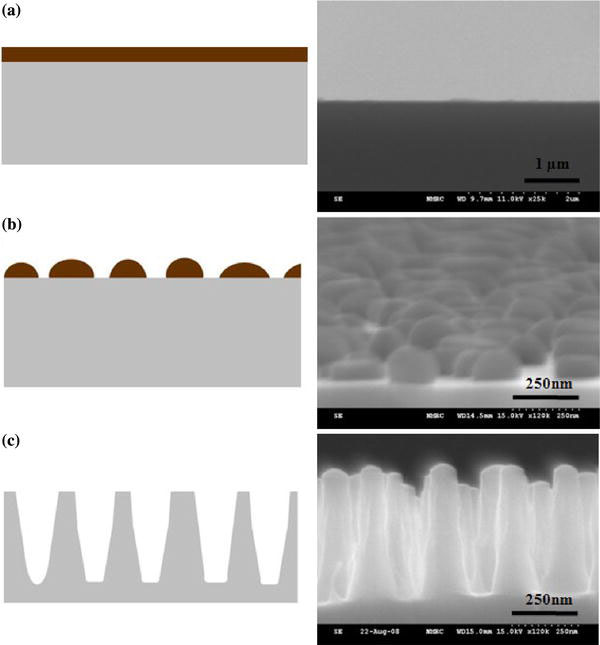
Fabrication process flow for tapered subwavelength antireflection structures:aPt/Pd alloy thin film deposition with a thickness of 10 nm;bthermally dewetted Pt/Pd alloy nanodot etch mask formed at an elevated temperature; andcformation of tapered subwavelength antireflection structures after RIE
Figure 2.
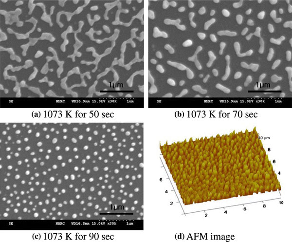
Thermal dewetting process of Pt/Pd alloy thin film for different heating time (a–c) and AFM image of dewetted nanodots (d)
The array of hemispherical nanodots is then used as an etch mask for CCP-RIE using Cl2and N2gases at the flow rate of 50 sccm for each and the RF power of 300 W. During the RIE process, the etch mask nanodots are also etched slowly, while the silicon is etched much faster. Moreover, since the nanodots are in hemispherical shape, the edges of nanodots are consumed faster in the RIE, exposing silicon under the nanodots. The size of nanodots becomes smaller as the RIE is proceeded, and the RIE time difference between the unmasked silicon and the silicon exposed later due to the nanodot etching makes the angled sidewall of SAS as shown in Fig. 1c.
Figure 3 shows SEM images of thermally dewetted Pt/Pd nanodots generated from three different film thicknesses. Figure 3b is magnified to fit the scale with other images. In Fig. 3a, c, and d, the Pt/Pd thin film is completely dewetted, but in Fig. 3b, the Pt/Pd thin film is not completely dewetted due to the insufficient thermal energy. As the thickness of Pt/Pd alloy thin film is increased, more thermal energy is needed for complete agglomeration and bigger Pt/Pd nanodots are formed. Thick Pt/Pd thin film leads to increased distance between nanodots and decreased number of nanodots in the same area. To achieve small reflectance, the period of antireflection structure should be less than the wavelength divided by the refractive index of substrate [16]. Considering that and from the repeated fabrication results, we decided to use 10 nm thickness Pt/Pd film for further etching process.
Figure 3.
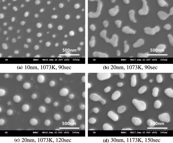
Thermal dewetting of Pt/Pd alloy thin film for different thickness
Figure 4a–d are the SEM images showing different height and shape of SAS for different etching time. As the etching time of RIE is increased from 60 to 110 s, the average height of tapered SAS is also increased from 230 to 470 nm. These samples are used to find the optimum fabrication process that produces the lowest reflectance. The etch rate of Si substrate in the experiment ranges from 4 to 5 nm/s. When a sample is etched for 110 s, the nanodot etch masks almost disappear and the average height of tapered SAS reaches the maximum of 470 nm. According to the SEM image in Fig. 1b and AFM graph in Fig. 2d, the typical height of Pt/Pd nanodots after thermal dewetting step falls within the range of 80–130 nm. Therefore, the calculated etching selectivity of Si substrate to Pt/Pd nanodots in our fabrication is about 4–5:1. In Fig. 4d after the RIE for 120 s, it is recognized that the height has been slightly reduced compared to the etching result for 110 s and the sidewall of tapered SAS is roughened. The reason for the reduced heights is that the tips of the structures are etched faster than the bottom of the structure when the nanodot etch masks are completely removed.
Figure 4.
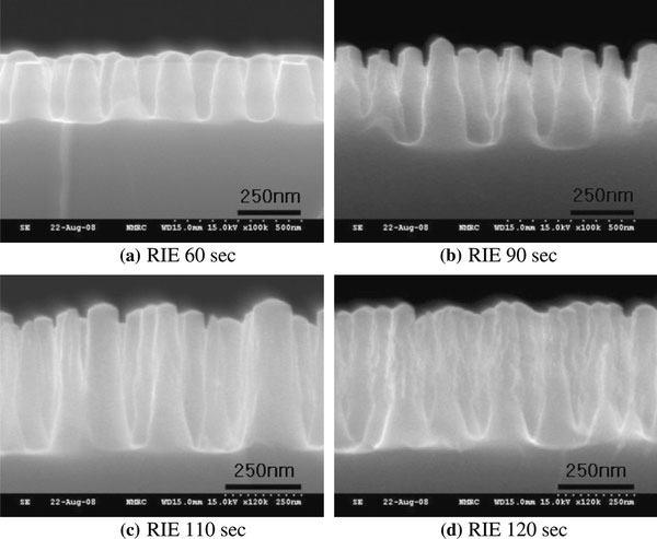
Side view of subwavelength antireflection structure array for different etching time. The measured average heights of SAS are:a230 nm,b370 nm,c470 nm, andd450 nm
Results and Discussion
For the repeated tests to find optimized recipe for thermal dewetting and RIE process, the Si wafer is broken into number of pieces and SAS were processed on them as shown in Fig. 5. The surface of the Si substrate with fabricated SAS array in Fig. 5a seems black due to the low reflectance while the bare Si wafer in Fig. 5b reflects the image of the camera that took this picture due to the high reflectance. However, considering the fabrication process is composed of only metal thin film deposition, heating and RIE without costly and time-consuming nano patterning steps such as electron beam lithography or nanoimprint lithography, the tapered SAS fabrication could be easily extended to wafer scale larger area. In Fig. 6, the SEM image of the angled view of the tapered SAS array fabricated in the large area is shown.
Figure 5.
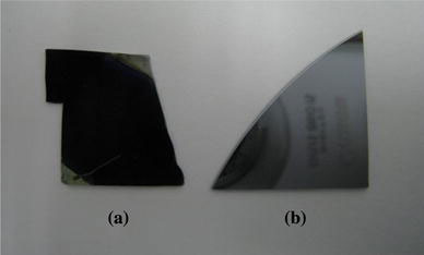
Si substrate (a) with fabricated SAS array is compared to bare Si substrate (b). Due to the low reflectance of the SAS array, substrate (a) seems completely black, while the highly reflective bare Si substrate (b) reflects the image of the camera that took this picture
Figure 6.
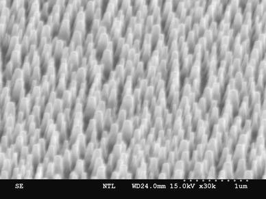
An SEM image (60° angle) of a high aspect ratio, large area subwavelength antireflection structures array
Since the tapered sidewall and height of SAS decide antireflective property, not only the formation of nanodot arrays by thermal dewetting but also the control of etching process is critical. RIE etching characteristics strongly depend on plasma density. As ion density and its energy differ between CCP-RIE and ICP (inductively coupled plasma)-RIE, they result in different etching rate and selectivity [17]. Since RIE with chlorinated plasma does not have large loading effect compared to CF4 plasmas, the chemical reaction during the silicon RIE in Cl2 plasma is not as much as in CF4 plasma [18]. Less chemical attack means the etching is relatively more physical, giving less chance of undercut. This is important for tapered SAS formation, and therefore, Cl2 plasma-based CCP-RIE is adopted in our fabrication. As shown in Figs. 4 and 6, the diameter of the tapered SAS continuously increases from top to bottom and thus the refractive index also continuously increases. Consequently, it is expected that the reflectance is very small for a wide range of wavelengths of light.
To assure the aforementioned, the reflectance of the fabricated SAS was measured by UV-VIS-NIR spectrophotometer (Varian Cary 500). Figure 7shows the reflectance measured as a function of the wavelengths of the light irradiated on five different sets of tapered SAS array with different heights generated by different etching time. The reflectance of bare silicon wafer is also presented for comparison. In the wavelength range from 350 to 1,800 nm, all of the differently processed samples show average reflectance under 5.5%. On the other hand, the measured average reflectance of bare Si wafers in the same wavelength range is 35%. In infrared range (700–1800 nm), the 420 nm height SAS array shows the smallest average reflectance value of 3.17%. In visible wave range (400–700 nm), the smallest reflectance is achieved on the SAS array with the heights of 370 nm and the average reflectance is 1.12%. Moreover, this sample shows extremely low reflectance value under 0.01% in a specific visible range of 570–650 nm. All samples show the smaller reflectance in visible wave range than in infrared or ultra violet wave range. This result is meaningful especially for solar cell applications since 46% of solar energy is in the visible wave range. In theory, the reflectance of the structure is expected to be decreased as the height of the structures increases. However, the measured average reflectance in the whole wavelength range from 350 to 1,800 nm decreases only to the height of 420 nm where the average reflectance is 2.80% and higher reflectance is observed for 450 and 470 nm structures. The measured average reflectance in visible and infrared range also shows the similar result. As a possible reason for this, it is presumed that the measured reflectance value could be slightly different depending on the specific location on the substrate due to the nonuniformity of the fabrication process. As described earlier, the reflectance is decided not only by the height of the SAS, but also by the period and taper angle. Since our SAS array is formed on a large area, it is possible that each fabrication step contains nonuniformity such as different Pt/Pd film thickness between center and edge of the substrate, which will lead to different sizes and periods of nanodot etch masks on the identical substrate. Nonuniform RIE may also result in the variation of the taper angle of SAS array between different locations of the substrate. Considering the further application of the SAS array as nano mold that could be replicated to polymers for low-cost antireflective surface formation, our monotonously tapered SAS is also advantageous, since previous works adopting thermal dewetting and etching produced mushroom-like shape of nanopillars with which demolding process is difficult.
Figure 7.
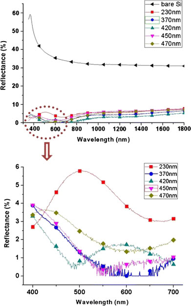
The reflectance measured as a function of the wavelengths of light irradiated on subwavelength antireflection structures with different height
Conclusions
In this paper, we presented simple and large area fabrication methods for tapered SAS without expensive and complicated nano patterning processes. By using the thermally dewetted Pt/Pd nanodots as etch mask and performing CCP-RIE with Cl2and N2gases, tapered SAS array was fabricated on large area silicon substrate. The monotonously tapered shape of fabricated SAS gives continuous and smooth increase of refractive index along the incident light path, resulting in very low reflectance <5.5% for 350–1,800 nm range of wavelength. Especially for visible light range, the measured reflectance of 1.12% is as low as the SAS fabricated by e-beam or nanoimprint lithography. The proposed method is expected to be applied not only to solar cell but also to optical and optoelectronic devices such as display screens and light sensors.
Acknowledgment
This research was supported by Nano R&D program through the Korea Science and Engineering Foundation funded by the Ministry of Science & Technology (2008-02916), and partially by a Grant-in-Aid for New and Renewable Energy Technology Development Programs from the Korea Ministry of Knowledge Economy (No. 2008-N-PV08-P-06-0-000).
References
- Kim JY, Lee K, Coates NE, Moses D, Nguyen T-Q, Dante M, Heeger AJ. Science. 2007. p. 222. COI number [1:CAS:528:DC%2BD2sXnsFaqtr4%3D]; Bibcode number [2007Sci...317..222K] [DOI] [PubMed]
- Kanamori Y, Sasaki M, Hane K. Opt. 1999. p. 1422. COI number [1:STN:280:DC%2BD2sjksV2hsg%3D%3D]; Bibcode number [1999OptL...24.1422K] [DOI] [PubMed]
- Kanamori Y, Roy E, Chen Y. Microelectron. 2005. p. 287. [DOI]
- Kobayashi H, Moronuki N, Kaneko A. Int. 2008. p. 25.
- Gombert A, Glaubitt W, Rose K, Dreibholz J, Blasi B, Heinzel A, Sporn D, Doll W, Wittwer V. Sol. Energy. 2000. p. 357. [DOI]
- Grann EB, Moharam MG, Pommet DA. J. Opt. Soc. Am. A. 1995. p. 333. Bibcode number [1995OSAJ...12..333G] [DOI] [PubMed]
- Toyota H, Takahara K, Okano M, Yotsuya T, Kikuta H. Jpn J. 2001. p. 747. [DOI]
- Yu Z, Gao H, Wu W, Ge H, Chou SY. J. Vac. Sci. Technol. B. 2003. p. 2874. COI number [1:CAS:528:DC%2BD2cXptFOgtw%3D%3D] [DOI]
- Lin G-R, Chang Y-C, Liu E-S, Kuo H-C, Lin H-S. Appl. 2007. p. 181923. Bibcode number [2007ApPhL..90r1923L] [DOI]
- Chiu CH, Peichen Y, Kuo HC, Chen CC, Lu TC, Wang SC, Hsu SH, Cheng YJ, Chang YJ. Opt. Express. 2008. p. 8748. COI number [1:CAS:528:DC%2BD1cXotlCitb0%3D]; Bibcode number [2008OExpr..16.8748C] [DOI] [PubMed]
- Wang S, Yu XZ, Fan HT. Appl. 2007. p. 061105. Bibcode number [2007ApPhL..91f1105W] [DOI]
- Nakanishi T, Hiraoka T, Fujimoto A, Saito S, Asakawa K. Microelectron. 2006. p. 1503. COI number [1:CAS:528:DC%2BD28XjsFGhtL8%3D] [DOI]
- Sun C-H, Jiang P, Jiang B. Appl. 2008. p. 061112. Bibcode number [2008ApPhL..92f1112S] [DOI]
- Xu H, Lu N, Qi D, Hao J, Gao L, Zhang B, Chi L (2008) Small. doi:10.1002/smll.200800282. [DOI] [PubMed]
- Lee J-M, Kim B-I. Mater. Sci. Eng. A. 2007. p. 769.
- Southwell WH. J. Opt. Soc. Am. A. 1991. p. 549. COI number [1:CAS:528:DyaK3MXhvFGjsbg%3D]; Bibcode number [1991OSAJ....8..549S] [DOI]
- Hikosaka Y, Nakamura M, Sugai H. Jpn J. 1994. p. 2157. COI number [1:CAS:528:DyaK2cXkt1Cmtb8%3D] [DOI]
- Schwartz GC, Schaible PM. J. 1979. p. 410. COI number [1:CAS:528:DyaE1MXksVyjsr4%3D]; Bibcode number [1979JVST...16..410S] [DOI]


