Abstract
The assembly of single-walled carbon nanotubes (SWCNTs) using the AC dielectrophoresis technique is studied theoretically. It is found that the comb electrode bears better position control of SWCNTs compared to the parallel electrode. In the assembly, when some SWCNTs bridge the electrode first, they can greatly alter the local electrical field so as to “screen off” later coming SWCNTs, which contributes to the formation of dispersed SWCNT array. The screening distance scales with the gap width of electrodes and the length of SWCNTs, which provides a way to estimate the assembled density of SWCNTs. The influence of thermal noise on SWCNTs alignment is also analyzed in the simulation. It is shown that the status of the array distribution for SWCNTs is decided by the competition between the thermal noise and the AC electric-field strength. This influence of the thermal noise can be suppressed by using higher AC voltage to assemble the SWCNTs.
Keywords: Single-walled carbon nanotubes (SWCNTs), AC dielectrophoresis, Simulation
Introduction
Since its discovery in 1991, carbon nanotubes (CNTs) have attracted great research interests due to its unique one-dimensional structure and outstanding properties [1]. A large amount of research has been conducted to explore both the fundamental properties [2-4] and application potentials for CNTs. In terms of applications, high-performance CNT-based field-effect transistors [5], solar cells [6], hazard gas detector [7], and DNA sensors [8] have been widely reported. It is also found that CNTs have excellent field emission properties [9,10]. With significant advantages over their traditional counterpart, CNTs are generally believed to be an ideal building block for the next generation electronics, optoelectronics, and high-performance sensors. However, the selectable and controllable placement and patterning of this nano-scale material has remained a challenge for their practical application. Common techniques to form aligned nanostructures include microwave plasma CVD [11], phase transformation [12], thermal oxidation [13], and electroless deposition [14]. Recently, researchers have shown that dielectrophoresis (DEP) is an efficient technique to manipulate carbon nanotubes [15,16]. With no functionalization, DEP has the potential of separating metallic-single-walled carbon nanotubes (SWCNTs) and semiconducting-SWCNTs [16], aligning carbon nanotubes between microelectrodes [17], and realizing large-scale manipulation [18]. Both experimental and theoretical work are conducted, most studies focus on the frequency-dependent DEP behavior of CNTs [19], and the translation and rotation of CNTs under electrical field [20]. However, the mechanisms for controllable patterning of CNTs between electrodes are not fully understood.
Here, the assembly of SWCNTs between electrodes is analyzed with the electrophoresis model. The influences of various factors including the electrode type, DEP voltage and thermal noise on the DEP assembly are taken into consideration. Besides, the influence of already deposited SWCNTs on the alignment of succeeding ones is also studied.
Theory
We model single carbon nanotube bundles as prolate ellipsoid with a = 500 nm, b = c = 10 nm. Its movement in suspending medium is governed by Langevin equation [21]:
| (1) |
where m is the mass of bundle, F the external force, and f the friction factor related to IPA’s viscosity η ( ) by [20]
| (2) |
In our modeling, F consists of two components: one is the deterministic DEP force due to electrical field generated by the electrodes; while the other is the random force induced by thermal noise in the surrounding medium. The latter leads to the well-known Brownian motion of microparticles.
DEP Movement
The DEP force is expressed in effective dipole approximation as [22]:
| (3) |
where  is the induced dipole moment on SWCNT-bundles. External field exert a torque on the dipole, and make the SWCNT-bundle align with the line of electrical field [23]. In this condition, let
  parallel to SWCNT-bundle’s major axis a, then Eq. 3 gives:
| (4) |
where 
 and
and  are the complex dielectric constant of SWCNT-bundles and suspending medium, respectively. Write ε* in the form of
  , we can derive that
| (5) |
In high frequency domain  (which is usually the condition for the dielectrophretic deposition of carbon nanotubes),
  is dominated by the dielectric constants over the conductivity, it can be simplified as:
| (6) |
Substitute this term into Eq. 3 gives:
| (7) |
Considering the mixture of s-SWCNT and m-SWCNT, it is estimated that  for SWCNT-bundles, while
  for IPA. For
  , the SWCNT-bundles experience positive DEP, which is illustrated in Fig. 1. As analyzed by previous papers [20], the SWCNT-bundles will be collected to the regions with the highest field strength, which is usually around the electrodes.
Figure 1.
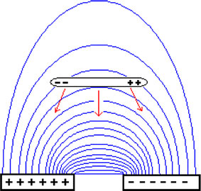
Carbon nanotubes subjected to positive dielectriphoresis. It is aligned with the field lines and moves towards the region with higher field strength
Brownian Motion
The influence of thermal noise in the medium increases when the size of micro-particles decreases. It can be described by the Brownian motion model. For SWCNT-bundles, in time interval ∆t, the Brownian displacement in each of the three coordinate axes can be expressed as [21]:
 |
(8) |
where KB is the Boltzmann constant, T the room temperature, f the friction factor of SWCNT-bundle, and Gi a Gaussian distributed random number.
The Solution of Langevin Equation
For DEP movement, the solution of Eq. 1can be approximated as:
| (9) |
where the characteristic time  is calculated to be 0.1 ns. For time intervals sufficient longer than α, Eq. 9can be approximated as:
| (10) |
Simulation
We use commercial finite-element software ANSYS 10.0 multiphysics [24] to solve the Poisson’s equation for (a) parallel electrode and (b) comb electrode, as shown in Fig. 2. The results are exported to Matlab for further processing. The distance between electrode pairs are both 1 μm, comparable to the length of SWCNT-bundle. The solution volume for the above two electrode structure are 9 × 6× 10 μm3 and 5 × 6× 10 μm3, respectively, the distance between neighboring grid point is 0.05 μm, which is precise enough for our simulation. Using Eq. 7, we can get the DEP force at every grid point.
Figure 2.
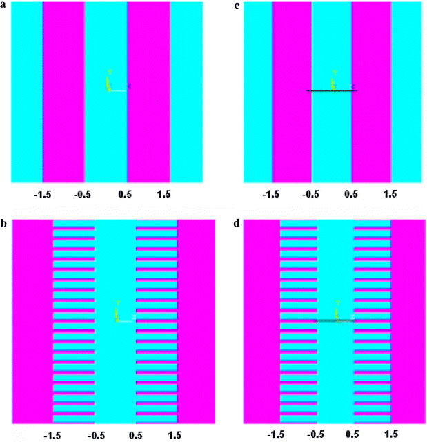
The electrode structure used in simulation:aparallel electrode;bcomb electrode;cparallel electrode with SWCNT-bundle bridged; anddcomb electrode with SWCNT-bundle bridged. The gap between the electrodes pairs for all structure is 1 μm. The width of the fingers and the space between the neighboring fingers in the comb electrode are, respectively, 100 nm and 0.3 μm
The movement of SWCNT-bundles is divided into a series of steps. For every time step, the terminal velocity is evaluated by Eq. 9. To avoid numerical errors, the time step is adjusted to make the space step constant, which means near regions with high field strength, the time step is effectively reduced. In our simulation, this time step is well above the characteristic time ∝, so the use of Eq. 9is justified. To account for Brownian motion, we superpose the Brownian displacement given by Eq. 7at every step.
To get the final SWCNT-bundles’ space distribution on the electrode, we initiate 1,000 randomly distributed SWCNT-bundles in the solution, and trace the movement of every bundle until it reaches the substrate. Considering the relatively low CNTs’ density in medium solution (in the order of μg/l in device applications), we neglect the interaction between SWCNT-bundles when they are suspended in the medium. However, once a bundle first attach to the electrode, it may severely alter the local electrical field structure. Thus, change the DEP movement of latter bundles. We numerically demonstrate this effect by solving the Poisson’s equation with one SWCNT-bundle bridge the electrode (Fig. 2c, d) and then use this field solution to simulate the subsequent SWCNT-bundles’ DEP process.
Result and Discussion
The simulated electrical field strengthE2for parallel and comb electrode is shown in Fig. 3. According to DEP theory for SWCNT-bundles,  is proportional to the gradient ofE2, so SWCNT-bundles will move toward the region with the highest field strength (the red zone in Fig. 3). Right above the surface of substrate (z = 0.2 μm), the highest electrical field appears at the edge of the electrode. A little higher (z = 0.5 μm), the highest field appears in the middle of the gap. Comparing Fig. 3a with b, we observe that comb electrode generates field map similar to its geometry structure. However, it is only for plane sufficient near the surface (z = 0.2 μm, which is comparable to the distance between neighboring finger tips). For the plane atz = 0.5 μm, comb electrode generate electrical field just like parallel electrode.
Figure 3.
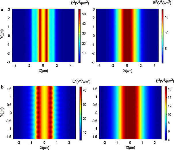
Simulated electrical field strength (E2) at the surface of the substrate (X–Yplane) foraparallel electrode andbcomb electrode. The left plot corresponds to the plane atY-coordinatez = 0.2 μm, the right plot corresponds to the plane atz = 0.5 μm
Because of its subtle electrical field structure, comb electrode provides possibilities to align SWCNT-bundles to desire cites on substrate. As shown in Fig. 3b, near the surface, the field varies periodically in the y-direction. Correspondingly, the SWCNT-bundles are supposed to assemble into array form with the same period. We simulate the distribution of 1,000 SWCNT-bundles after DEP for both parallel and comb electrode. As shown in Fig. 4, this distribution perfectly reflects the field structure generated by the electrode. For parallel structure, almost all the bundles locate in the gap between the two adjacent electrodes, and it is uniformly distributed. This indicates that parallel electrode is efficient to capture SWCNT-bundles. When the length of bundle is larger than the width of the gap (1 μm in Fig. 4a), there is a high ratio of SWCNT-bundles bridged the electrode, which is desired in electrical characterization and device fabrication. In fact, there are reports using parallel electrode DEP to construct CNT-based field-effect transistors, thin film transistors and solar cells. However, because of the random distribution of SWCNT-bundles, the parallel electrode is not a good choice to construct large number of devices based on single bundle of SWCNTs. Comb electrode, as shown in Fig. 4b, can assemble SWCNT-bundles into array structure. The SWCNT-bundles are collected in the region between countering fingertips because of its higher local field strength. In our simulation, the distance between neighboring fingers is 0.3 μm, and the distribution of SWCNT-bundles basically has the same period. Confirmed by previous experiments [21], our simulation indicates that comb electrode has the potential to realize large-scale assembly of SWCNT devices.
Figure 4.
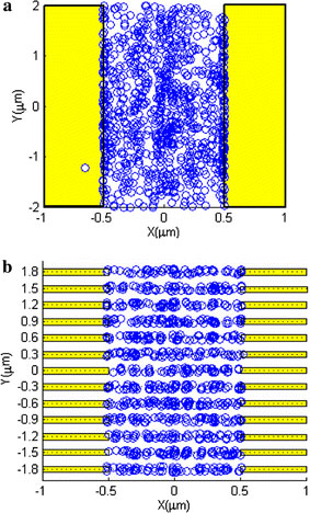
Simulated distribution of 1,000 SWCNT-bundles foraparallel electrode andbcomb electrode. The yellow regions represent the electrodes and the blue circles represent the centroids of SWCNT-bundles
When suspended in the solution medium, the interaction between SWCNT-bundles can be neglected because of relatively low density (in the order of μg/l). On the other hand, when the interaction between two SWCNT-bundles are taken into account, we are actually dealing with the interaction between the two dipole moments  and
and  For one SWCNT-bundle, the interaction force is due to the field created by the dipole moment of another SWCNT-bundle. This interaction force can be expressed as
  where
where  is the field created by dipole moment
  So generally, this interaction force is a secondary effect, and will not influence the DEP movement due to the fact that the DEP force produced by external field dominates. The case that the interaction between SWCNT-bundles will play a main role is when the external field
  is uniform, in which
  and there is no DEP movement. In our simulation, the use of microelectrodes will cause the generation of strong non-uniform electrical fields. So, the interaction between SWCNT-bundles will not change the results of our simulation.
Whenever one single bundle bridges the electrode, it can greatly change the local electrical field structure. The mechanism can be explained as follows: When no SWCNT-bundle bridges the electrodes, the voltage drop exists across the gap of the electrode pairs. After a SWCNT-bundle bridges the electrodes, the contact resistance of metal–nanotube junction plays a dominant role and absorbs most of the voltage drop [25]. As a result, the main body of SWCNT-bundle is nearly equipotential. Therefore, when the SWCNT-bundle bridges the electrodes, the local potential distribution is changed, thereby changing the local electrical field. We numerically demonstrate this effect by simulate the electrical field structure for both parallel and comb electrode when one SWCNT-bundle bridged the electrodes. As shown in Fig. 5, for both parallel and comb electrode structure, the highest field region (red zone) is intercepted by the presence of bridged SWCNT-bundle at Y = 0. Away from the bundle, the field structure remains the same as in Fig. 4. Several experiments confirmed this “screen” effect of bridged SWCNT-bundle to latter bundles in DEP process. For parallel electrode, SWCNT-bundles tend to form dispersively aligned parallel array, with an average distance between neighboring bundles. While for comb electrode, this effect ensures that for every fingertip electrode pair, there is only one bundle bridged. The results are consistent with our earlier experimental research [26,27]. Using modified electrical field for CNT-bridged electrode, we simulate the corresponding distribution of latter SWCNT-bundles, as shown in Fig. 6. For parallel electrode, there is approximately a 0.4-μm (−0.2 μm to +0.2 μm) wide region where there’s almost no SWCNT-bundles landed. Outside this region, the bundles are uniformly distributed as in Fig. 4. For comb electrode, very few bundles land between the fingertip pair at Y = 0 μm. The other fingertip pairs are not affected by the “screen effect”, probably because the distance between neighboring pairs (0.3 μm) exceed the “screening length”, which is 0.2 μm in Fig. 6a.
Figure 5.
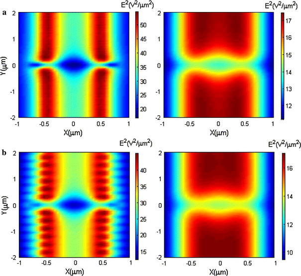
With one SWCNT-bundle bridge the electrode atY = 0 μm, simulated electrical field strength (E2) at the surface of the substrate (X–Yplane) foraparallel electrode andbcomb electrode. The left plot corresponds to plane atz = 0.2 μm, the right plot corresponds to plane atz = 0.5 μm
Figure 6.
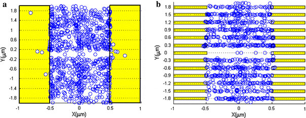
Simulated distribution of 1,000 SWCNT-bundles foraparallel electrode andbcomb electrode. In both electrodes, there is one SWCNT-bundle pre-bridged atY = 0 μm. The yellow regions represent the electrodes and the blue circles represent the centroids of SWCNT-bundles
The “screening effect” in DEP process makes the controllable patterning of carbon nanotubes possible. In our simulation, for 1-μm electrode gap and 1-μm long SWCNT-bundle, the screening length is about 0.2 μm. This provides estimation for the upper limit of the density of DEP patterned carbon nanotubes array. Because the electrostatics scales with the size of the objects, we can anticipate the shorter screening length if we reduce the gap of electrodes as well as the length of SWCNT-bundles. That means if we use 100-nm-long SWCNT-bundle and keep the size ratio of all the structures constant, the screening length will be reduced to 20 nm. Unfortunately, for smaller SWCNT bundles, the influence of the thermal noise increases. Stronger Brownian motion will disturb the deterministic DEP movement. We simulate the DEP process for the 100-nm-scale case: the gap of electrodes and the length of SWCNT-bundles are reduced to 100 nm; the size ratio of all structures is kept constant. The results are shown in Fig. 7, in which the peak-to-peak voltage (V) is 1 V, with the electrical field in the medium kept invariant as that for the 1-μm-scale case. The movement of SWCNT-bundle is randomized by the thermal noise even if it is very close to the electrode surface. WhenV = 5 V, the DEP force is increased so as to overcome the Brownian motion near the electrode. The corresponding distribution of SWCNT-bundles for the comb electrode at 100 nm scale is simulated, as shown in Fig. 8. It indicates that when peak-to-peak voltage is 1 V, the thermal noise disarranges the array distribution while the peak-to-peak voltage of 5 V can overcome the influence of thermal noise and retain the array distribution.
Figure 7.
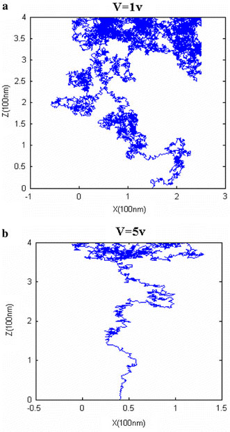
The DEP movement of SWCNT bundles in the 100-nm-scale case foraV = 1 V andbV = 5 V
Figure 8.
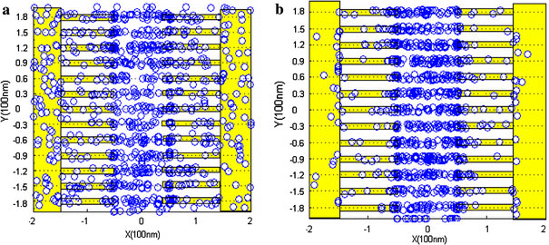
Simulated distribution of 1,000 SWCNT-bundles for the comb electrode with the peak-to-peak voltage ofa1 V andb5 V. The yellow region represent electrodes, the blue circles represent the centroids of SWCNT-bundles
Conclusion
The assembly of SWCNTs on the electrodes using the DEP method has been studied theoretically. The influences of electrode type, electrode voltage, thermal noise, and as-bridged nanotubes on the results of DEP assembly are analyzed. The results suggest that: (1) although the parallel and comb electrode are both effective electrode structures to align the SWCNTs, the comb electrode has a better position control of SWCNTs than the parallel electrode; (2) once a SWNCT bundle bridges on the electrode, it will change the local electrical field and “screen off” the SWCNTs that approach later; for parallel electrode this effect results in the formation of dispersed SWCNT array, while for comb electrode it guarantees that one fingertip pair collects only one SWCNT bundle; (3) the density of DEP assembled array is limited by the “screening length”, which scales with the gap width of electrodes and the length of SWCNT bundle; and (4) the thermal noise has an important influence on the DEP assembly of SWCNTs, which is more significant for the smaller electrode structures and shorter SWCNTs; by increasing the AC voltage, this influence can be effectively eliminated.
Misc
Changxin Chen and Yang Lu contributed equally to this work.
Contributor Information
Changxin Chen, Email: chen.c.x@sjtu.edu.cn.
Yafei Zhang, Email: yfzhang@sjtu.edu.cn.
Acknowledgment
This work is supported by National Natural Science Foundation of China No. 60807008, Shanghai International Science and Technology Cooperation Foundation No. 08520741500, Shanghai Science and Technology Grant No. 0752nm015, National Natural Science Foundation of China No. 50730008 and National Basic Research Program of China No. 2006CB300406.
References
- Avouris P, Appenzeller J, Martel R, Wind SJ. Proc. IEEE. 2003. p. 1772. COI number [1:CAS:528:DC%2BD3sXpt1GqsLs%3D] [DOI]
- White CT, Todorov TN. Nature. 1998. p. 240. COI number [1:CAS:528:DyaK1cXjtlymtLY%3D]; Bibcode number [1998Natur.393..240W] [DOI]
- Nakanishi T, Bachtold A, Dekker C. Phys. Rev. B. 2002. p. 073307. Bibcode number [2002PhRvB..66g3307N] [DOI]
- Egger R. Phys. 1999. p. 5547. COI number [1:CAS:528:DC%2BD3cXnt1OmsQ%3D%3D]; Bibcode number [1999PhRvL..83.5547E] [DOI]
- Javey A, Kim H, Brink M, Wang Q, Ural A, Guo J, McIntyre P, McEuen P, Lundstrom M, Dai H. Nat. 2002. p. 241. COI number [1:CAS:528:DC%2BD38Xpt1amur8%3D]; Bibcode number [2002NatMa...1..241J] [DOI] [PubMed]
- Chen CX, Lu Y, Kong ES, Zhang YF, Lee ST. Small. 2008. p. 1313. Cover paper. [DOI] [PubMed]
- Kong J, Franklin NR, Zhou C, Chapline MG, Peng S, Cho K, Dai H. Science. 2000. p. 622. COI number [1:CAS:528:DC%2BD3cXovVWgtA%3D%3D]; Bibcode number [2000Sci...287..622K] [DOI] [PubMed]
- Staii C, Johnson AT, Chen JM, Gelperin A. Nano Lett. 2005. p. 1774. COI number [1:CAS:528:DC%2BD2MXosVGgsbw%3D] [DOI] [PubMed]
- Rakhi RB, Sethupathi K, Ramaprabhu S. Nanoscale Res. 2007. p. 331. COI number [1:CAS:528:DC%2BD2sXpslegtr8%3D]; Bibcode number [2007NRL.....2..331R] [DOI] [PMC free article] [PubMed]
- Srivastava SK, Vankar VD, Kumar V, Singh VN. Nanoscale Res. 2008. p. 205. COI number [1:CAS:528:DC%2BD1cXhsVyhtr%2FF]; Bibcode number [2008NRL.....3..205S] [DOI]
- Jian SR, Chen YT, Wang CF, Nanoscale Res. 2008. p. 230. COI number [1:CAS:528:DC%2BD1cXhsVyhtrzO]; Bibcode number [2008NRL.....3..230J] [DOI]
- Yan C, Xue DF. Adv. 2008. p. 1055. COI number [1:CAS:528:DC%2BD1cXlt1WmtL0%3D] [DOI]
- Liu J, Xue DF. Adv. 2008. p. 2622. COI number [1:CAS:528:DC%2BD1cXptVOrsLc%3D]; Bibcode number [2005JMatR..20.2622L] [DOI]
- Yan CL, Xue DF. Electrochem. 2007. p. 1247. COI number [1:CAS:528:DC%2BD2sXlslGit7o%3D] [DOI]
- Chen XQ, Saito T, Yamada H, Matsushige K. Appl. 2001. p. 3714. COI number [1:CAS:528:DC%2BD3MXjvF2mtLs%3D]; Bibcode number [2001ApPhL..78.3714C] [DOI]
- Krupke R, Hennrich F, Löhneysen H, Kappes MM. Science. 2003. p. 344. COI number [1:CAS:528:DC%2BD3sXls1yhs7c%3D]; Bibcode number [2003Sci...301..344K] [DOI] [PubMed]
- Kumar MS, Lee SH, Kim TY, Kim TH, Song SM, Yang JW, Nahm KS, Suh EK. Solid-State Electron. 2003. p. 2075. [DOI]
- Krupke R, Hennrich F, Weber HB, Kappes MM, Löhneysen H. Nano Lett. 2003. p. 1019. COI number [1:CAS:528:DC%2BD3sXltF2rur4%3D] [DOI]
- Krupke R, Hennrich F, Kappes MM, Löhneysen H. Nano Lett. 2004. p. 1395. COI number [1:CAS:528:DC%2BD2cXlsF2itbw%3D] [DOI]
- Peng N, Zhang Q, Li J, Liu N. J. 2006. p. 024309. Bibcode number [2006JAP...100b4309P] [DOI]
- Morgan H. Electrokinetics AC Colloids and Nanoparticle. PA Research Studies Press, Philadelphia; 2003. [Google Scholar]
- Morgan H, Green NG. J. 1997. p. 279. [DOI]
- Jones TB. Electromechanics of Particles. Cambridge University Press, Cambridge; 1995. [Google Scholar]
- www.ansys.com
- Chen Z, Appenzeller J, Knoch J, Lin Y, Avouris P. Nano Lett. 2005. p. 1497. COI number [1:CAS:528:DC%2BD2MXlsVelu7k%3D] [DOI] [PubMed]
- Chen CX, Zhang YF. J. Phys. D Appl. Phys. (Berl) 2005. p. 172. Bibcode number [2006JPhD...39..172C] [DOI]
- Chen CX, Xu D, Kong ES, Zhang YF. IEEE Electron. 2006. p. 852. Bibcode number [2006IEDL...27..852C] [DOI]


