Abstract
The photovoltaic properties of solar cell based on the blends of poly[2-methoxy-5-(2-ethylhexoxy-1,4-phenylenevinylene) (MEH-PPV), fullerene (C60), and ZnCdTe-alloyed nanocrystals were investigated. Comparing the spectral response of photocurrent of the MEH-PPV:C60(+ZnCdTe) nanocomposite device with that of the devices based on MEH-PPV:C60and pristine MEH-PPV, one can find that the nanocomposite device exhibits an enhanced photocurrent. In comparing the composite devices with different ZnCdTe:[MEH-PPV + C60] weight ratios of 10 wt% (D1–1), 20 wt% (D1–2), 40 wt% (D1–3), and 70 wt% (D1–4), it was found that the device D1–3exhibits the best performance. The power conversion efficiency (η) is improved doubly compared with that of the MEH-PPV:C60device.
Keywords: ZnCdTe, Alloy, Nanocrystals, Heterojuction, Solar cell
Introduction
In the past decades, polymer solar cells have attracted more and more scientific attention due to their advantages, such as low cost, light weight, easy fabrication, and the possibility to fabricate flexible devices, compared with inorganic solar cells [1-5]. However, the limited dissociation of photoexcitation at weak electric field and poor charge transport in the polymer affects their applications. Along with the discovery of photo-induced fast charge transfer between conjugated polymer and C60, the possibility of all plastic photovoltaic cells with conjugated polymers and C60 derivatives as basic materials resulted in a large short-circuit current and a high power conversion efficiencies [6-9]. Although more effective dissociation of photogenerated excitons can occur on the interfaces of polymer and C60 in polymer–fullerene bulk heterojunction solar cells, electron mobility is still poor and imbalance between electron and hole results in carrier recombination during transmission in solar cells. A good photoconductive device requires not only efficient charge separation, but also efficient transport of charge carriers to the electrodes. The blends of conjugated polymer and inorganic nanocrystals have exhibited excellent photoconductive properties because the inorganic semiconductor nanocrystals can efficiently dissociate the photogenerated excitons and have high electron mobility [10]. Moreover, the dependence of the band gap of nanocrystals on particle radius can make it absorb light with tunable wavelengths and the compensated light harvest of nanocrystal and conjugated polymer enlarged the absorption range [1,11,12]. In recent years, binary nanocrystals such as CuS, ZnO, TiO2, CdS, and CdSe have been investigated extensively for their technological applications in optoelectronics [10,13-17], but few study have been reported for the application of ternary-alloyed nanocrystals synthesized in aqueous solutions in the solar cells.
The band gap of ternary-alloyed nanocrystals can be adjusted by controlling not only particle radius but also the composition of ternary-alloyed nanocrystals [18-20]. Most of devices based on polymer–fullerene blend configurations suffer from reduced Voc because of the large band offset between the electron donor and acceptor materials. In order to increase the Voc and efficiency in such devices, the donor–acceptor band offset must be optimized. This has been previously demonstrated in polymer–fullerene blend devices, where the electron affinity of the fullerene derivative was modified leading to a change in the Voc[21]. The application of ZnCdTe-alloyed nanocrystals can provide continuous control of the band offset over a large range by controlling not only particle radius but also the composition and leads to increased Voc values in hybrid devices.
We prepared ZnCdTe nanocrystals in aqueous solutions according to the method that have been reported [18]. Then, the phase-transfer method was used to transfer ZnCdTe nanocrystals into a xylene solution, which is combined with the blend of MEH-PPV + C60 in xylene to fabricate composite devices. The comparison of the spectral response of photocurrent of the MEH-PPV:C60 (+ZnCdTe) nanocomposite device with that of the pristine MEH-PPV and MEH-PPV:C60 devices was made. The results from voltage–current characteristics showed that the conversion efficiency of devices with the 40% weight ratios of ZnCdTe nanocrystals is doubled compared with the devices without blending ZnCdTe nanocrystals.
Experiment
Synthesis of ZnCdTe-Alloyed Nanocrystals
ZnCdTe nanocrystals were synthesized according to the method we have reported [18]. In brief, thioglycolic acid was added into the mixed precursor solutions of Cd(CH3COO)2 2H2O and Zn(CH3COO)2 2H2O, which was adjusted to pH = 9 by using the solution of 2 mol/L sodium hydroxide, followed by adding a freshly prepared oxygen-free NaHTe solution with vigorous stirring under nitrogen atmosphere. Then, the solution was heated to 105 °C for 3 h, and ZnCdTe-alloyed nanocrystals were formed. Finally, ZnCdTe-alloyed nanocrystals were precipitated by addition of isopropyl alcohol and then centrifuged when the solution was cooled to room temperature. The ZnCdTe powder was obtained after drying in N2 atmosphere.
Fabrication of the Nanocomposite Device
The ZnCdTe-alloyed nanocrystals were redissolved in distilled water. Cetyltrimethyl ammonium bromide (CTAB) was used to precipitate the alloyed nanocrystals as the surfactant. And then the precipitation was re-dispersed in xylene after being dried and combined with the xylene solution of MEH-PPV:C60with different nanocryshals concentrations. ITO-coated glass substrate was first cleaned for sample preparation by detergent and distilled water in an ultrasonic bath, respectively. Poly(3,4- ethylenedioxythiophene):poly(styrenesulfonate) (PEDOT:PSS) was spin-coated on top of ITO-coated glass substrates as the polymer anode to smoothen the substrate surface, and this was followed by thermal treatment for several minutes.
The active layers of the solar cells were prepared from the blends of MEH-PPV:C60(6:1.5 mg/mL) and ZnCdTe-alloyed nanocrystals with different weight ratio in xylene. The weight ratios of ZnCdTe to MEH-PPV:C60are 10 wt% (D1–1), 20 wt% (D1–2), 40 wt% (D1–3), and 70 wt% (D1–4), respectively. After stirring for about 3 h, the blends of MEH-PPV:C60and ZnCdTe nanocrystals in xylene were spin-coated onto the PEDOT:PSS substrates. The thickness of a photoactive layer was around 100 nm. Al electrodes were deposited onto the blend active layers in sequence through a shadow mask on top of the active layer by vacuum thermal evaporation as cathode. The shadow mask defines an active area of 2 mm2. For the sake of comparison, the undoped MEH-PPV:C60device (D1–0) was fabricated with the same processes as mentioned. The obtained structure of devices is ITO/PEDOT:PSS/MEH-PPV:C60(+ZnCdTe)/Al. Figure 1shows the schematic device structure.
Figure 1.
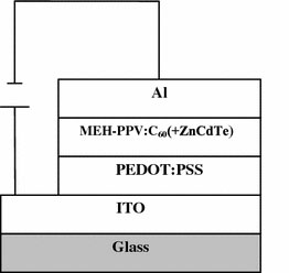
Schematic diagrams of the devices structure
Measurements
The spectral response of photocurrent and current–voltage curves were recorded by a Keithley 2410 source measure unit both in the dark and under illumination. The incident light from a Xe lamp was passed through a monochromator in SPEX Fluorolog-3 spectrophotometer to select a wavelength at 500 nm with an intensity of 16.7 mW/cm2. The spectral responses of photocurrent were also obtained by illumination with the light from a Xe lamp, which was passed through a monochromator to select wavelengths between 400 and 700 nm. Transmission electron microscopy (TEM) images were performed on a HITACHI H-700 transmission electron microscope. High-resolution transmission electron microscopy (HR-TEM) study was carried out on a PHILIPS TECNAI F30 microscope at an acceleration voltage of 300 kV. X-ray photoelectron spectra (XPS) were recorded by a VG MKII X-ray photoelectron spectrometer with monochromatized Al Ka radiation as the excitation source. X-ray diffraction (XRD) pattern was measured by Philips APD-10 X-ray diffractometer with graphite monochromatized Cu Ka radiation (λ = 0.154178 nm).
Results and Discussion
Figure 2a displays a typical TEM image of the synthesized ZnCdTe-alloyed nanocrystals. The particles are nearly spherical and the average size is less than 10 nm.
Figure 2.

Characterization of synthesized ZnCdTe-alloyed nanocrystals.aTEM image,bHRTEM image,cXPS spectra,dthe XRD patterns (the vertical lines below indicate the diffractions from the standard pattern of cubic ZnCdTe nanocrystals), andethe absorption spectrum of the ZnCdTe-alloyed nanocrystals
HR-TEM image of ZnCdTe nanocrystals (Fig. 2b) shows regular lattice fringes with a spacing of 0.35 nm, which corresponds to the (111) plane of ZnCdTe.
Figure 2c shows the XPS spectra of ZnCdTe nanocrystals. The features at 405 and 412 eV for the ZnCdTe nanocrystals are known to stem from Cd 3d. The peaks at 573 and 583 eV are from Te 3d, and the peak of 1021 and 1045 eV also appear with the presence of Zn 2p states, respectively. This result can confirm the existence of cadmium, zinc, and tellurium species in the ZnCdTe nanocrystals.
Figure 2d shows the XRD pattern of the obtained alloyed nanocrystals. XRD patterns show obvious broadening phenomena, which indicate the small size of the alloyed nanocrystals [18]. The crystal structures of ZnCdTe can be assigned as cubic structures, with the presence of characteristic (111), (220), and (311) peaks in the XRD patterns.
Figure 2e shows the absorption spectrum of ZnCdTe alloy nanocrystals. The absorption peak of ZnCdTe nanocrystals locates at 450 nm.
Figure 3 shows the spectral response of photocurrent of the hybrid device for wavelengths from 400 to 700 nm with the nanocomposite structure of ITO/PEDOT:PSS/MEH-PPV:C60 (+ZnCdTe)/Al. For the sake of comparison, the spectral response of photocurrent of the devices with single layer of MEH-PPV and with blend layer of MEH-PPV:C60 are also shown. As shown in Fig. 3, the photocurrent of the MEH-PPV:C60 (+ZnCdTe) nanocomposite device is more enhancive than that of MEH-PPV and MEH-PPV:C60 devices, which result from photogeneration and transport mechanism of charge carriers in MEH-PPV:C60 (+ZnCdTe) nanocomposite device [22]. Due to the poor electron mobility in the polymer and the lack of interfaces for dissociation of photogenerated excitons, the weak photocurrent is obtained in single layer of MEH-PPV device. The photocurrent for MEH-PPV:C60 (+ZnCdTe) nanocomposite device is more enhanced than that of the MEH-PPV:C60 device. In nanocomposite devices, the inorganic nanocrystals easily aggregate to form some regions surrounded by regions of polymers. With enough content of nanocrystals in the composite film, these regions will grow to form a connected network in the film. In the homogeneous film, the exciton–dissociation interface between polymer and ZnCdTe nanoparticles cross through the nanocomposite film and much more electrons photogenerated by the incident photon through the device are contributed to the photocurrent. Consequently, the enhanced photocurrent response is obtained in MEH-PPV:C60 (+ZnCdTe) nanocomposite device [13].
Figure 3.
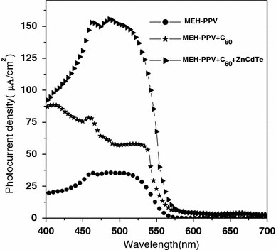
Spectral response of photocurrent of a pristine MEH-PPV device, a MEH-PPV:C60device, and a MEH-PPV:C60 (+ZnCdTe) nanocomposite device containing 40 wt% ZnCdTe nanocrystals
Figure 4 shows the characteristics of photocurrent of five devices based on MEH-PPV:C60 (0%, D1–0) and MEH-PPV:C60 (+ZnCdTe) blends with different weight ratios (10%, 20%, 40%, 70%) of ZnCdTe under illumination. It can be observed clearly that with the increasing ratio of the ZnCdTe-alloyed nanocrystals, the short-circuit current density (Jsc) values increase gradually, but when the ratio is up to 70%, Jsc get decreased. Appropriately increasing ZnCdTe content in the blend film will generate more percolation pathways, which should help the transport of electrons and increases the photocurrent [1,10], so the maximum output power increase. We obtained the highest Jsc value when the ratio of ZnCdTe is 40 wt% in the blend film. In addition, the built-in potential for carrier injection into the devices is also an important factor in increasing the photocurrent. The increasing built-in potential can improve the photocurrent of the devices. As well known, the trend of built-in potential can be reflected in the change of the open-circuit voltage (Voc) of devices. A similar trend to Jsc is observed in the Voc (as shown in Table 1 and Fig. 5), only when the ratio is 10%, the Voc is almost unchanged. With the low nanocrystal blending, the Voc of MEH-PPV:C60-only device is preserved until a threshold representing the formation of ZnCdTe-alloyed nanocrystals networks across the device is reached. At this point, the Voc rises to approach that of the complete heterojunction [23]. With the formation of ZnCdTe-alloyed nanocrystals networks by increasing the concentration of crystals, they will be many surface states on the surface of the ZnCdTe. The Fermi level of aluminum is partially pinned to the surface states close to the lowest unoccupied energy levels of ZnCdTe (as shown in Fig. 6). [12,22]. In many bulk inorganic semiconductors and metal junctions, the Fermi level of the metal is pinned to the surface states of the semiconductor within the band gap [12]. ZnCdTe-alloyed nanocrystals substitute the cathode to form a new limitation for built-in potential (as shown in Fig. 6). Therefore, the Voc increased, when the concentration of ZnCdTe is high enough. But if the concentration is too high, the JscVocPmax, FF, and η decline sharply. The reasons for these cell parameters declines come from many factors. There are two reasons to be considered. First, excessively increasing ZnCdTe in the blend film leads to the decrease of the polymer content, which may decrease the contribution of MEH-PPV to the light absorption and destroy the interpenetrating pathway for holes transport, thus resulting in a decrease of η values [1,10]. Second, due to the limit of solubility of ZnCdTe-alloyed nanocrystals in polymer, the nanocomposite device with the 70% high blending concentration has displayed the uniformity of nanocoposite film. The dispersion of ZnCdTe-alloyed nanocrystals in MEH-PPV + C60 blend cannot be well unified with the increasing alloyed nanocrystals concentration [10], which leads to decreasing of FF of nanocomposite devices. The concentration of alloyed nanocrystals plays an important role in optimizing photovoltaic properties of the nanocomposite devices.
Figure 4.
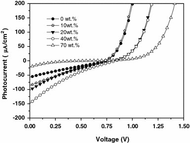
Characteristics of photocurrent of MEH-PPV:C60 device and MEH-PPV:C60 (+ZnCdTe) nanocomposite device with different ZnCdTe ratios under illumination at the wavelength of 500 nm with the intensity of 16.7 mW/cm2
Table 1.
Photocurrent–voltage characteristics of composite devices with MEH-PPV:C60 (+ZnCdTe) as the active layer, along with the undoped MEH-PPV:C60 (D1–0) device in comparison of the composite devices with different ZnCdTe:[MEH-PPV + C60] weight ratios of 10 wt% (D1–1), 20 wt% (D1–2), 40 wt% (D1–3), and 70 wt% (D1–4)
| D1–0 | D1–1 | D1–2 | D1–3 | D1–4 | |
|---|---|---|---|---|---|
| Jsc(μA/cm2) | 57.1 | 87.0 | 101.6 | 148.7 | 21.2 |
| Voc(V) | 0.74 | 0.74 | 0.81 | 0.84 | 0.51 |
| FF | 0.23 | 0.22 | 0.18 | 0.18 | 0.12 |
| Pmax(μW/cm2) | 10.04 | 14.09 | 14.30 | 21.91 | 1.35 |
| η (%) | 0.060 | 0.084 | 0.086 | 0.13 | 0.0081 |
Vocopen-circuit voltage,Jscshort-circuit current density (under λ = 500 nm with the light intensity of 16.7 mW/cm2),FFfill factor,Pmaxthe maximum output power, and η the power conversion efficiency
Figure 5.
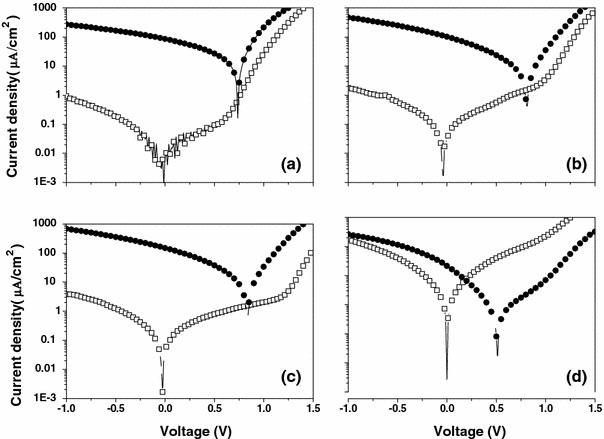
The current–voltage curves in the dark (open squares) and under illumination (closed circles) of 16.7 mW/cm2at 500 nm of devices with different ZnCdTe ratiosaD1–1,bD1–2,cD1–3, anddD1–4
Figure 6.
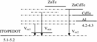
Schematic ofVocin ITO/PEDOT:PSS/MEH-PPV:C60(+ZnCdTe)/Al blend film devices with concentration of ZnCdTe. For an undoped MEH-PPV:C60device,Vocis dominated by the system of MEH-PPV:C60(Voc1). With the increasing concentration of ZnCdTe, the limitation for resultingVoc, corresponding to an MEH-PPV:C60 (+ZnCdTe) composite device, at the negative electrode gradually shifts towards the LUMO energy level of ZnCdTe (Vocn). When the LUMO of acceptor (ZnCdTe) completely acts as the limitation forVoc, the resultingVoccan be expressed byVoc2
Conclusion
In summary, we have presented the photovoltaic properties of the MEH-PPV:C60(+ZnCdTe nanocrystals) composite device. The experimental results show that the devices with blending ZnCdTe nanocrystals exhibited an enhanced photocurrent. We investigated the effect of different ZnCdTe:[MEH-PPV + C60] weight ratios on the performance of the devices. When the weight ratio is not higher than 40%, the short current densityJscand the open-circuit voltageVocincreased with the increasing weight ratio of ZnCdTe nanocrystals. The characteristics of the devices degraded when the concentration of ZnCdTe nanocrystals is too high up to 70%. The power conversion efficiency is doubled and the short current is close to triple by blending ZnCdTe nanocrystals with the concentration of 40%.
Acknowledgment
This work was supported by Trans-Century Training Program Foundation for the Talents of Natural Science by the State Education Commission, Key Project of Chinese Ministry of Education (no. 105041), National Natural Science & Foundation Committee of China (NSFC) (Project nos. 90401006 and 10434030), State key project of basic research (2003CB314707) and the Key Laboratory of Specially Functional Materials and Advanced Manufacturing Technology, South China University of Technology, Ministry of Education, China.
References
- Zhou Y, Li YC, Zhong HZ, Hou JH, Ding YQ, Yang CH, Li YF. Nanotechnology. 2006. p. 4041. COI number [1:CAS:528:DC%2BD28XhtFChsL7J]; Bibcode number [2006Nanot..17.4041Z] [DOI] [PubMed]
- Yu G, Gao J, Hummelen JC, Wudl F, Heeger AJ. Science. 1995. p. 1789. COI number [1:CAS:528:DyaK2MXhtVSiurjF]; Bibcode number [1995Sci...270.1789Y] [DOI]
- Brabec CJ, Sariciftci NS, Hummelen JC. Adv. 2001. p. 15. COI number [1:CAS:528:DC%2BD3MXhs12kt78%3D] [DOI]
- Brabec CJ. Sol. Energy Mater. Sol. Cells. 2004. p. 273. COI number [1:CAS:528:DC%2BD2cXksVGhsbs%3D] [DOI]
- Hoppe H, Sariciftci NS. J. 2004. p. 1924. COI number [1:CAS:528:DC%2BD2cXlslSqtrg%3D]; Bibcode number [2004JMatR..19.1924H] [DOI]
- Yang CH, Qiao J, Sun QJ, Jiang KJ, Li YL, Li YF. Synth. 2003. p. 1521. COI number [1:CAS:528:DC%2BD3sXktFOht7s%3D] [DOI]
- Sariciftci NS, Smilowitz L, Heeger AJ, Wudl F. Science. 1992. p. 1474. COI number [1:CAS:528:DyaK3sXmtVKhtg%3D%3D]; Bibcode number [1992Sci...258.1474S] [DOI] [PubMed]
- Sariciftci NS, Braun D, Zhang C, Srdanov VI, Heeger AJ, Stucky G, Wudl F. Appl. 1993. p. 585. COI number [1:CAS:528:DyaK3sXhtlOiur0%3D]; Bibcode number [1993ApPhL..62..585S] [DOI]
- Lioudakis E, Othonos A, Alexandrou I. Nanoscale Res. 2008. p. 278. COI number [1:CAS:528:DC%2BD1cXhsVyhtr3N]; Bibcode number [2008NRL.....3..278L] [DOI] [PMC free article] [PubMed]
- Tang AW, Teng F, Jin H, Gao YH, Hou YB, Liang CJ, Wang YS. Mater. 2007. p. 2178. COI number [1:CAS:528:DC%2BD2sXktF2jsrw%3D] [DOI]
- Greenham NC, Peng XG, Alivisatos AP. Phys. Rev. B. 1996. p. 17628. COI number [1:CAS:528:DyaK2sXkt1Ojug%3D%3D]; Bibcode number [1996PhRvB..5417628G] [DOI] [PubMed]
- Huynh UW, Dittmer JJ, Teclemariam N, Milliron DJ, Alivisatos AP. Phys. Rev. B. 2003. p. 115326. Bibcode number [2003PhRvB..67k5326H] [DOI]
- Jin H, Hou YB, Tang AW, Meng XG, Teng F. Chin. 2006. p. 693. COI number [1:CAS:528:DC%2BD28XjtVCktb0%3D]; Bibcode number [2006ChPhL..23..693J] [DOI]
- Huynh WU, Dittmer JJ, Alivisatos AP. Science. 2002. p. 29. [DOI] [PubMed]
- Sirimanne PM, Tributsch H. J. 2004. p. 1789. COI number [1:CAS:528:DC%2BD2cXktVWqsrw%3D]; Bibcode number [2004JSSCh.177.1789S] [DOI]
- Yu K, Chen JH. Nanoscale Res. 2009. p. 1. COI number [1:CAS:528:DC%2BD1MXht1Kgs7w%3D]; Bibcode number [2009NRL.....4....1Y] [DOI]
- Hullavarad SS, Hullavarad NV, Karulkar PC, Luykx A, Valdivia P. Nanoscale Res. 2007. p. 161. COI number [1:CAS:528:DC%2BD2sXktVartLs%3D]; Bibcode number [2007NRL.....2..161H] [DOI]
- Wang Y, Hou YB, Tang AW, Feng B, Li Y, Liu J, Teng F. J. Cryst. Growth. 2007. p. 19. COI number [1:CAS:528:DC%2BD2sXhtFejs7%2FE]; Bibcode number [2007JCrGr.308...19W] [DOI]
- Zhong XH, Zhang ZH, Liu SH, Han MY, Knoll WG. J. Phys. Chem. B. 2004. p. 15552. COI number [1:CAS:528:DC%2BD2cXntlKksLo%3D] [DOI]
- Zhong XH, Feng Y, Knoll WG, Han MY. J. 2003. p. 13559. COI number [1:CAS:528:DC%2BD3sXnvFSjt7k%3D] [DOI] [PubMed]
- Olson DC, Shaheen SE, White MS, Mitchell J, Test FAM, Collins RT, Ginley DS. Adv. 2007. p. 264. COI number [1:CAS:528:DC%2BD2sXhslGktr8%3D] [DOI]
- Li Y, Hou YB, Jin H, Shi QM, Zhang LX. Chin. 2007. p. 2654. COI number [1:CAS:528:DC%2BD2sXhtFaktrfN]; Bibcode number [2007ChPhL..24.2654L] [DOI]
- Gur I, Fromer NA, Chen CP, Kanaras AG, Alivisatos AP. Nano Lett. 2007. p. 409. COI number [1:CAS:528:DC%2BD28XhtlGku7rP]; Bibcode number [2007NanoL...7..409G] [DOI] [PubMed]


