Abstract
We propose a superlattice consisting of graphene and monolayer thick Si sheets and investigate it using a first-principles density functional theory. The Si layer is found to not only strengthen the interlayer binding between the graphene sheets compared to that in graphite, but also inject electrons into graphene, yet without altering the most unique property of graphene: the Dirac fermion-like electronic structure. The superlattice approach represents a new direction for exploring basic science and applications of graphene-based materials.
Keywords: Graphene, Silicon, Superlattice, Density functional theory, Intercalated graphite, Dirac fermion, MBE, FET
The success of extracting a graphene sheet from a graphite crystal a few years ago has triggered enormous interest in exploring the unique physics and novel applications [1,2]. However, to be able to study the intrinsic properties of graphene or make an electronic device, the single atomic sheet is often required to sit or be grown on a semiconductor or metallic substrate [3,4]. The interaction between the graphene and substrate almost inevitably perturbs the intrinsic property of pristine graphene, for instance, leading to bandgap opening in the otherwise zero bandgap graphene [5]. Bandgap opening might be convenient for the electronic application such as making transistors [6]; it nevertheless destroys perhaps the most unique aspect of graphene—the cone-shape electronic structure at the Dirac or K point of the two-dimensional (2D) Brillion zone (BZ) of graphene. It has recently been shown that in potassium intercalated graphite, KC8, the electronic structure of graphene near the Dirac point can be largely preserved, except for a 1.35 eV upward shift in Fermi level (EF) from that at the touching point of the conduction and valence band in graphene, as a result of charge transfer from potassium to graphene layers [7]. Potassium is a well-known donor that is often used along with other alkali metals for intercalated graphite compounds (IGCs) for the purpose of improving the in-plane conductivity of graphite [8]. IGCs are also targeted as battery, electrode and catalytic materials, carbon fibers, etc. However, despite four decades effort, none of them has yet made substantial impact because these IGCs are not sufficiently uniform and robust in meeting more rigid standards for electronic device applications. Another major issue that has hindered the practical application and even the basic research of the intercalated graphite is their poor stability [8]. Therefore, there is a vital need to form a graphene-based “superstructure” to provide mechanical robustness and chemical stability.
Superlattice, proposed by Esaki and Tsu in 1970, [9] has been a major force in providing man-made solids with unique properties that are not readily available in nature, such as Bloch oscillation at THz frequency, negative differential conductance for amplifier, quantum cascade lasers, IR detectors. It is not generally known that another major motivation that drove Esaki and Tsu to man-made superlattices was to increase the size of the basic unit, such as a double barrier resonant tunneling structure, so that real devices may be constructed and controlled from the standpoint of optimum size and power handling. A periodic structure is basically the best option that we know to mimic a large solid. The concept of the superlattice has been extended far beyond the originally proposed systems, from the extreme of monolayer superlattices, [10] in terms of the layer thickness to another extreme, the inorganic-organic hybrid superlattices representing a drastically different chemical bonding [11]. The Graphene/Silicon (Gr/Si) superlattice to be explored in this work represents an example of a superlattice structure with uniqueness in both layer thickness and chemical bonding. Intercalation is not an efficient and sufficiently precise method for making the proposed superlattice. We propose instead using molecular beam epitaxy (MBE) to assemble the periodic structure layer by layer. An added reason to explore the possibility of binding the graphene sheets together with Si is obviously because Si is the backbone of the current electronic technology.
Two primary discoveries of the present investigation are (1) Gr/Si superlattice exhibits significantly stronger interlayer bonding than graphite, and (2) the electronic band structure near the grapheme K point is practically unperturbed by the Si layer, but with significant electron transfer from the Si layer into the graphene layer.
We apply a first-principles density functional theory (DFT), within the local density approximation (LDA), to study the structural and electronic properties of the proposed Gr/Si superlattice, and the 2D Si structure as the second component of the superlattice. The DFT-LDA level theory has been well documented to be quite adequate for describing the structural properties of graphite near its equilibrium configuration [12], and capable of offering basic understanding for its electronic band structure (subjecting to the well-known LDA error in the bandgap) [13], although higher-order theories (e.g., GW) are needed for quantitative analyses of experimental data involving many-body effects [7,14]. A plane-wave pseudopotential code, PEtot [15], is used. A kinetic energy cutoff of 60 Ry is used in conjunction with norm-conserving pseudopotentials. For the structural calculation, BZ sampling is performed using 16 × 16 × 10 k-point grids for the 3D structures (Gr/Si and graphite crystals) and 16 × 16 × 1 for the 2D structures (graphene and Si sheets). For the 3D structure, equilibrium in-plane and out-of-plane lattice constants, a and c, are determined by searching for the local minimum of the total energy Etot(a,c). For the 2D structure, a is obtained by minimizing Etot(a), using a periodic structure with a vacuum space of 15 Å for graphene and 20 Å for Si [16]. With the obtained lattice parameters, 50 × 50 × 10 or 50 × 50 × 1 k-point grids are then used for the band structure calculations, resulting in more accurate Fermi energies (typically converging to within a few meV).
The first question to ask: what would be the Si structure that best matches the graphene structure? Graphitic Si, a silicon equivalent of AB graphite, has a theoretical in-plane lattice constant a = 4.07 Å, [16] which corresponds to a bond length of 2.35 Å, the same as that of the diamond structure. Given the fact that the graphene lattice constant a is only 2.46 Å, the lattice mismatch is huge (65%) between a graphene-like Si and graphene. However, a 30o-rotated structure (√3x√3R30) could in principle yield a closely lattice-matched superlattice, but with lower symmetry. The primary interest of this work is the next higher symmetry structure. We notice that the center-to-center separation of the hexagons in graphene is quite close to the Si bond length (4.5% difference). Therefore, Si should sit well at the hollow site of graphene, as in the cases of many IGCs, forming a 2D equilateral triangular lattice. The chemical formula for such a superlattice will be SiC2. As a matter of fact, SiC2 molecules are known to exist for many decades in multiple isomers with a cyclic form to be the energetically most stable [17]. What we have proposed is simply an ordered ensemble of SiC2 molecules. The superlattice could also simply be viewed as another form of Silicon Carbide. We find that the triangular Si layer itself is indeed a metastable state with Etot = −107.0 eV/atom (0.917 eV/atom higher than that in the diamond phase) and aSi = 2.4271 Å. The lattice constant of this 2D lattice turns out to be closer to that of the graphene than those of the other two forms of Si, providing the rationale for an in-depth study of the Gr/Si superlattice.
Structural Properties
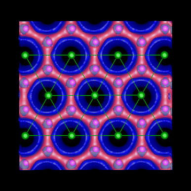
For the AB graphite, our calculation yields aAB = 2.4395 Å and cAB = 6.6589 Å, agreeing very well with the extrapolated 0 K experimental results: 2.4589 Å and 6.6720 Å (deviations of only −0.77 and −0.19%) [18]. The lattice constant of graphene, aGr = 2.43935 Å, is slightly smaller than that of AB graphite, which could be understood by visualizing that one of the C atoms in the B layer sits above the hollow site of the A layer, causing a small expansion of the C ring in the A layer. For the AA graphite, aAA = 2.43927 Å is practically the same as that of graphene, but the separation of the graphene sheets is 8.4% larger than that of the AB graphite or cAA = 3.6105Å (similar to a previous report [19]), indicating weaker interlayer coupling for the AA stacking. The lattice mismatch between graphene and the Si sheet is only 0.5%, and the formation of the Gr/Si superlattice yields an in-plane lattice constant aGr/Si = 2.4363 Å in between aSi and aGr, forming an ideal strained-layer superlattice, with cGr/Si = 7.2662 Å. The C-Si layer separation is only slightly larger than cAA (by 0.63%), given the fact that Si is substantially larger than C. Figure 1 shows the atomic structure of the superlattice, viewed along the c axis, overlaid with the ground state total charge density. It shows more charge on the graphene plane than in the Si plane, because of the C/Si ratio = 2 and more extended charge distribution along the c axis for Si.
Figure 1.

The atomic structure of graphene/Si superlattice, with Si atoms on top, projected onto the graphene plane, overlaid with two contour plots of the total charge density. The contour of the 80% maximum (red) reveals the charge distribution on graphene, and the 20% contour (blue, drawn with 40% opacity) shows the charge distribution on the Si sheet
The interlayer binding energy of the graphite and superlattice is defined as Eb = (Etot − ΣiEtot,i)/N, where Etot is the total energy for the final system,Etot,i is for the individual layer, and N is the total number of atoms per unit cell. For the AB graphite, the LDA calculations seem converging to Eb ≈ 20–25 meV/atom, [16,20-22] whereas the experimental results are in the range of 23–52 meV/atom [23-25]. Our results are 24.4 and 15.0 meV/atom, respectively, for the AB and AA graphite. We find a significant enhancement in the interlayer binding for the Gr/Si superlattice, being Eb = 35.1 meV/atom. It is interesting to note that the hypothetic graphitic Si has a substantially stronger interlayer binding (175 meV/atom) than that of graphite [16]. It has been pointed out that the LDA calculation might underestimate the binding energy, and the improved value with the many-body effect included becomes 56 meV/atom for the AB graphite [22]. Therefore, the actual binding strength of the Gr/Si superlattice may be somewhat stronger than our current LDA result. We note that the √3x√3R30-based superlattice would have a somewhat smaller interlayer binding energy (32.8 meV/atom).
Electronic Properties
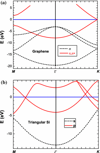
We first produce the electronic structure of graphene and the Si layer, using aGr/Si. The result for graphene is shown in Fig. 2(a), which resembles the results of previous DFT-LDA calculations: a zero bandgap semiconductor with linear dispersions near K point [8]. The in-plane binding for the triangular Si sheet is somewhat different from that of graphene: Si is sixfold coordinated, instead of threefold for C in graphene. If assuming the in-plane binding remains as sp2, then there would be only one electron/bond, implying a metallic behavior. With this assumption, the pz orbit would also be half-occupied. One possibility for it to be a semiconductor is to have two electrons going to the s-like band and the other two to the pz-like band. Fig. 2(b) shows the actual calculated band structure. It turns out that the band structure is semiconductor-like in the k-space surrounding the Γ point. However, toward the zone boundary, the band structure becomes metallic, and thus the Si sheet is a semi-metal. At the Γ point, the lowest state is s-like, and the second state is pz-like, but the third is a mixture of all the three p states, leading to our labeling them as s-like and p-like.
Figure 2.

The band structures of graphene (a) and the Si layer (b). Fermi level is set to zero
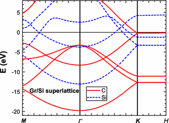
Shown in Fig. 3 is the band structure of the Gr/Si superlattice. There are a few important findings: (1) the dispersion curves can be divided into two groups, respectively, from the graphene and Si sheet, indicating that the coupling is relatively weak; (2) the dispersions of the graphene-like bands near the K point retain the same type of linear dispersion as in the graphene, because it is a property dictated by the symmetry rather than the strength of the coupling; [26] (3) EF moves to 234 meV above the Dirac point of graphene, indicating that electrons are transferred from Si to graphene, which is also corroborated by the downward shift of EF with respect to the Si derived states in the vicinity of EF. We may say approximately the band structures of the two materials move rigidly against each other as a whole. The relative shift is a result of leveling EF for the whole system as a combined effect of work function difference and the interface dipole formation, similar to what happens in the metal-semiconductor as well as metal-graphene interface [27,28]. There are, however, internal changes within each group: for instance, the separation at the Γ point between the lowest and the second lowest band decreases by 0.245 eV for the graphene group. Along the direction of the c axis, the dispersion of the highest valence band is 69 meV between K and H, slightly larger than the 38 meV in the AB graphite. A significant difference lies in that in the graphite the highest valence band provides the electron conductivity near the K point and hole conductivity near the H point, whereas in the Gr/Si superlattice, the valence band states are fully occupied throughout the K-H line of BZ. Therefore, the only conducting carrier type in the graphene sheet is electron, due to the electron pocket occupying the π* band states close to the K point. The number of the electron transferred into graphene is estimated to be 4 × 10⁻³e/Si, much less than 0.8e/K in KC8[7]. However, the number of conducting electrons, occupying the states approximately within kT from EF, are actually about the same for SiC2 and KC8, despite Si being isovalent to C. Note that the number of electrons in the graphene layer can be further modified by an external electric field applied along the superlattice stacking direction, which is a ready-made structure for a field-effect transistor (FET) or a stack of FETs if employing the similar scheme of forming a quantum cascade laser using a superlattice. Also, there are plenty of other possible replacements for the Si sheet to offer diverse novel properties of graphene/X superlattices, X may include such as BN, SiO2, P, and even organic molecules.
Figure 3.

Band structure of graphene/Si superlattice (EF = 0).Solid and dashedcurves are, respectively, for the bands derived from graphene and the Si layer
In summary, we have shown that the Gr/Si superlattice indeed has the improved mechanical stability and enhanced transport property. Considering other intercalants in a graphene-based superlattice using a layer by layer growth, we anticipate that this type of superlattice may lead to a future class of man-made materials for electronics.
Acknowledgments
We thank CRI for partial support, NERSC for computer resources, L.-W. Wang and S.-H. Wei for helpful discussions.
Open Access
This article is distributed under the terms of the Creative Commons Attribution Noncommercial License which permits any noncommercial use, distribution, and reproduction in any medium, provided the original author(s) and source are credited.
References
- Geim AK, Novoselov KS. Nat. 2007. p. 183. COI number [1:CAS:528:DC%2BD2sXit1Khtrg%3D]; Bibcode number [2007NatMa...6..183G] [DOI] [PubMed]
- Katsnelson MI. Mater. Today. 2007. p. 20. COI number [1:CAS:528:DC%2BD2sXht1arsL4%3D] [DOI]
- de Heer WA, Solid State Commun. 2007. p. 92. COI number [1:CAS:528:DC%2BD2sXmt1yhtrc%3D]; Bibcode number [2007SSCom.143...92D] [DOI]
- Li XS, Science. 2009. p. 1312. COI number [1:CAS:528:DC%2BD1MXms12gtbY%3D]; Bibcode number [2009Sci...324.1312L] [DOI] [PubMed]
- Zhou SY, Nat. 2007. p. 770. COI number [1:CAS:528:DC%2BD2sXhtFWhtrnJ]; Bibcode number [2007NatMa...6..770Z] [DOI] [PubMed]
- Freitag M. Nat. 2008. p. 455. COI number [1:CAS:528:DC%2BD1cXptlKntLY%3D] [DOI] [PubMed]
- Gruneis A, Phys. Rev. B. 2009. p. 075431. COI number [1:CAS:528:DC%2BD1MXhtFWjtr7F]; Bibcode number [2009PhRvB..80g5431G] [DOI]
- Dresselhaus MS, Dresselhaus G. Adv. 2002. p. 1. COI number [1:CAS:528:DC%2BD38XjsVKnsrs%3D]; Bibcode number [2002AdPhy..51....1D] [DOI]
- Esaki L, Tsu R. IBM Res. 1970. p. 61. COI number [1:CAS:528:DyaE3cXnt1aitw%3D%3D] [DOI]
- Ge WK, J. 1994. p. 163. COI number [1:CAS:528:DyaK2cXjtlCjt70%3D] [DOI]
- Huang XY. J. 2003. p. 7049. COI number [1:CAS:528:DC%2BD3sXjs1Ggtbo%3D] [DOI] [PubMed]
- Girifalco LA, Hodak M. Phys. Rev. B. 2002. p. 125404. COI number [1:CAS:528:DC%2BD38XisVCiurs%3D]; Bibcode number [2002PhRvB..65l5404G] [DOI]
- Jansen HJF, Freeman AJ. Phys. Rev. B. 1987. p. 8207. COI number [1:CAS:528:DyaL2sXkvVCisbc%3D]; Bibcode number [1987PhRvB..35.8207J] [DOI] [PubMed]
- Park C-H, Phys. 2009. p. 076803. COI number [1:CAS:528:DC%2BD1MXitlagtLo%3D]; Bibcode number [2009PhRvL.102g6803P] [DOI] [PubMed]
- Wang L-W. http://hpcrd.lbl.gov/~linwang/PEtot/PEtot.html http://hpcrd.lbl.gov/~linwang/PEtot/PEtot.html
- Wang Y, Scheerschmidt K, Gsele U. Phys. Rev. B. 2000. p. 12864. COI number [1:CAS:528:DC%2BD3cXjsVWjurk%3D]; Bibcode number [2000PhRvB..6112864W] [DOI]
- Grev RS, Schaefer HF. J. 1984. p. 3552. COI number [1:CAS:528:DyaL2cXhvFyjuro%3D]; Bibcode number [1984JChPh..80.3552G] [DOI]
- Baskin Y, Meyer L. Phys. 1955. p. 544. COI number [1:CAS:528:DyaG28XhvVKnsA%3D%3D]; Bibcode number [1955PhRv..100..544B] [DOI]
- Wang L-W. Phys. Rev. B. 2002. p. 153410. COI number [1:CAS:528:DC%2BD38XjtV2mtr8%3D]; Bibcode number [2002PhRvB..65o3410W] [DOI]
- Schabel MC, Martins JL. Phys. Rev. B. 1992. p. 7185. COI number [1:CAS:528:DyaK38XlvFyksL8%3D]; Bibcode number [1992PhRvB..46.7185S] [DOI] [PubMed]
- Charlier JC, Gonze X, Michenaud JP. Europhys. 1994. p. 403. COI number [1:CAS:528:DyaK2MXitleqs7Y%3D]; Bibcode number [1994EL.....28..403C] [DOI]
- Spanu L, Sorella S, Galli G. Phys. 2009. p. 196401. COI number [1:CAS:528:DC%2BD1MXhtl2rsr7P]; Bibcode number [2009PhRvL.103s6401S] [DOI] [PubMed]
- Girifalco LA, Lad RA. J. 1956. p. 693. COI number [1:CAS:528:DyaG2sXhtFagsg%3D%3D]; Bibcode number [1956JChPh..25..693G] [DOI]
- Benedict LX, Chem. 1998. p. 490. COI number [1:CAS:528:DyaK1cXit1Sktrg%3D]; Bibcode number [1998CPL...286..490B] [DOI]
- Zacharia R, Ulbricht H, Hertel T. Phys. Rev. B. 2004. p. 155406. COI number [1:CAS:528:DC%2BD2cXktVGqtLg%3D]; Bibcode number [2004PhRvB..69o5406Z] [DOI]
- Slonczewski JC, Weiss PR. Phys. 1958. p. 272. COI number [1:CAS:528:DyaG1cXlsVertw%3D%3D]; Bibcode number [1958PhRv..109..272S] [DOI]
- Bennett AJ, Duke CB. Phys. 1967. p. 578. COI number [1:CAS:528:DyaF2sXlt1Srs74%3D]; Bibcode number [1967PhRv..162..578B] [DOI]
- Khomyakov PA, Phys. Rev. B. 2009. p. 195425. COI number [1:CAS:528:DC%2BD1MXmvF2rtbk%3D]; Bibcode number [2009PhRvB..79s5425K] [DOI]


