Abstract
We report the fabrication of heterostructure white light–emitting diode (LED) comprised of n-ZnO nanotubes (NTs) aqueous chemically synthesized on p-GaN substrate. Room temperature electroluminescence (EL) of the LED demonstrates strong broadband white emission spectrum consisting of predominating peak centred at 560 nm and relatively weak violet–blue emission peak at 450 nm under forward bias. The broadband EL emission covering the whole visible spectrum has been attributed to the large surface area and high surface states of ZnO NTs produced during the etching process. In addition, comparison of the EL emission colour quality shows that ZnO nanotubes have much better quality than that of the ZnO nanorods. The colour-rendering index of the white light obtained from the nanotubes was 87, while the nanorods-based LED emit yellowish colour.
Keywords: ZnO nanotubes, Light-emitting diodes, Electroluminescence, Lightning, White light sources
Introduction
Zinc oxide has substantive advantages including the quests for LEDs and laser diodes [1,2] because of its wide band gap (~3.37 eV) and large exciton-binding energy (60 meV). Also, deep level defects (intrinsic and extrinsic) in ZnO can lead to an emission band covering the whole visible spectrum [3]. Furthermore, the optoelectronic properties of ZnO can be tuned by changing its morphology, composition, crystalline structure, orientation and the growth conditions [4,5]. The development of ZnO homojunction diodes is rare due to the lack of authentic procedure to grow high-quality p-type ZnO [6,7]. As an interesting alternate, the deposition of n-ZnO nanostructures on different p-type semiconductors is quite frequent to utilize the electronic and optical advantages offered by heterostructure devices. Gallium nitride (GaN) is the most suitable p-type material having wide band gap, wurtzite crystal structure and least mismatching (~1.8%) in lattice constants [8]. Till date, white LEDs are being fabricated either by using phosphors or by mixing several coloured light. However, there are significant barriers for the large-scale applications of both processes. The former is associated with a strong reduction in device efficiency due to the problems such as low durability and requirement of relatively high fabrication temperatures for organic and inorganic phosphors, respectively. On the other hand, the latter requires the complex mixing or doping schemes, and exponential decay in emission power occurs with the increase in temperature, resulting in substantial change in colour stability [9-11]. Recently, ZnO NTs/Au Schottky LED has been reported covering an emission spectrum between 400 and 600 nm [12]. Here, we report a promising route towards the fabrication of heterostructure LED by exploiting the ZnO NTs for white light–emitting applications. As ZnO NTs have excellent optoelectronic properties due to their large surface to bulk ratio with high porosity and significant amount of surface states giving rise to broadband emission covering the whole visible spectrum. This technique has several advantages, e.g. cheap, simple and environmentally benign in comparison with other techniques.
Experimental
ZnO nanorods were aqueous chemically synthesized on p-GaN substrate by using low-temperature approach. The GaN substrate containing ZnO nanorods was cut into two pieces. One of them was used as a reference sample, while the second half was dipped in potassium chloride (KCl) aqueous solution for the trimming of ZnO nanorods into nanotubes using optimized parameters, as previously reported [13], except the immersion time which was shortened intentionally to reduce the etching depth of ZnO NTs. Both samples were further processed to fabricate the LEDs by depositing the ohmic contact on p-GaN film by evaporating Ni/Au bilayers of thicknesses 20/40 nm, respectively. Shipley-1805 photoresist film was homogeneously deposited as an insulating layer by spin coating to fill the space between the ZnO NTs and uncovered area of the p-GaN substrate. Selective etching of the photoresist was carried out using a reactive ion etching in order to expose the tip of ZnO NTs ~ few nanometres. Finally, top contacts on ZnO were made by evaporating Ti/Au bilayers of thicknesses 20/30 nm, respectively.
Results and Discussion
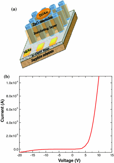
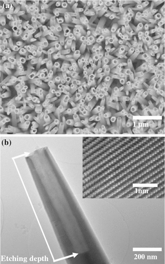
Figure 1a demonstrates the schematic diagram of the fabricated n-ZnO NTs/p-GaN white LED. The current–voltage (I–V) characteristics curve of the n-ZnO NTs/p-GaN heterojunction exhibits a nonlinear increase in the current under forward bias as shown in Fig. 1b. Literally, good rectification was obtained with a threshold voltage of ~5 V. The threshold voltage is higher than the bandgap of ZnO (3.37 eV), mainly owing to the high resistivity of the p-type GaN layer. The dimensional and morphological evaluations of the ZnO NTs are studied by scanning electron microscopy (SEM) as shown in Fig. 2a. It is carefully observed that the diameter of the ZnO NTs is 100-150 nm with the wall thickness of 25–40 nm where the average length of the NTs is about 1.7 μm. The structural characterization is further studied by low- and high-resolution transmission electron microscopy (TEM) to investigate the etching depth and the crystallinity of the ZnO NTs (Fig. 2b). The etching depth of ZnO NTs has been intentionally kept between 700 and 900 nm to protect the p–n junction of the heterostructure.
Figure 1.

a Schematic 3D illustration of n-ZnO NTs/p-GaN heterostructures LED device b I–V characteristics of the ZnO NTs–based light-emitting diode with threshold voltage ~5 V
Figure 2.

a SEM image of ZnO NTs b low-resolution TEM image of single ZnO NT showing the tubular structure with etching depth. The inset is a high-resolution TEM showing the single-crystalline structure of the ZnO NTs
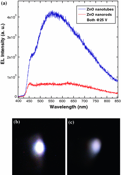
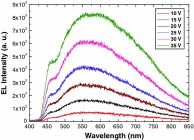
The EL spectra have been measured by applying a forward bias voltage at room temperature, and emitted light has been detected from the top electrode. Figure 3a shows the EL spectra of ZnO nanotubes and nanorods-based heterostructure LEDs at a bias voltage of 25 V. It is clear that the emission from the ZnO nanotubes has higher intensity than that of ZnO nanorods. The emission spectrum of ZnO nanotubes exhibits relatively weak violet–blue emission and dominating broadband emission peaks, centred at around 450 and 560 nm, respectively. The origin of the former peak (450 nm) is still under debate and generally attributed to two possible sources. According to the first opinion, the emission peak is due to the transition from zinc interstitial to zinc vacancy [14,15]. The radiative recombination related to deep Mg acceptor levels is another possible source of the violet–blue emission [16,17]. ZnO NTs offer relatively low turn-on voltage and higher current growth rate than ZnO nanorods [12]. Hence, there will be more injection of electrons from the conduction band of ZnO towards the Mg-doped p-GaN, which could be the reason to enhance the rate of radiative recombination to emit the higher violet–blue emission peak for the ZnO nanotubes. The latter peak can be imputed to the injection of the holes from p-GaN towards ZnO NTs and their recombination with defect states in the ZnO NTs, which results in the increased spectral width of the deep band emission (425–750 nm). ZnO NTs also possess a large number of surface states due to the high surface to bulk ratio and high porosity. In addition, etching process may introduce more surface states and bulk defects resulting in a wide band of visible spectrum [13]. Owing to these properties, ZnO nanotubes have the ability to emit more intense white light when compared to ZnO nanorods. Figure 3b, c show lighting photographs of emission from LED devices based on ZnO NTs and ZnO nanorods, respectively, at the same bias value. It is clear from the images that the light emission from the n-ZnO NTs/p-GaN LED is stronger when compared to the emission from n-ZnO nanorods/p-GaN. Besides the broad emission, the fabricated LED reveals enhancement and stability in the EL intensity of n-ZnO NTs/GaN. The enhancement in emission intensity with gradual increase in the applied voltage (Fig. 4) can be attributed to activation of more radiative recombination centres in ZnO NTs. No significant change either in the shape or position of the EL spectrum with increasing the applied voltage has been observed. This is in contrast to recently reported ZnO NTs/Au Schottky LED, where the position and shape of the emission spectrum are observed to be highly dependent on the applied bias [12].
Figure 3.

a Room temperature EL spectra of ZnO/GaN LEDs under forward bias from nanotubes (blue) and nanorods (red). Digital images of the LED devices taken at the same applied voltage from b ZnO nanotubes c ZnO nanorods
Figure 4.

Room temperature EL spectra of ZnO NTs/GaN LEDs under forward bias voltages (10, 15, 20, 25, 30 and 35 V) showing broadband emission peaks without any distinct shift
Conclusion
In conclusion, white light–emitting diode based on n-ZnO NTs/p-GaN was developed by using simple, cost-efficient and low-temperature approach. The fabricated LED showed higher current density and stronger EL emission peaks centred at 450 and 560 nm when compared to the LED comprised of ZnO nanorods. The enhanced EL intensity of the visible band (425–750 nm) emission from the ZnO NTs is due to their high porosity, large surface area and the high density of recombination centres at the surface. The use of ZnO NTs provided the prospects to explore the potential of white inorganic light–emitting diode with superior performance.
Open Access
This article is distributed under the terms of the Creative Commons Attribution Noncommercial License which permits any noncommercial use, distribution, and reproduction in any medium, provided the original author(s) and source are credited.
References
- Zhu H, Shan CX, Yao B, Li BH, Zhang JY, Zhang ZZ, Zhao DX, Shen DZ, Fan XW, Lu YM, Tang ZK. Adv. 2009. p. 1613. COI number [1:CAS:528:DC%2BD1MXltFGiurg%3D] [DOI]
- Chuang RW, Wu RX, Lai LW, Lee CT. Appl. 2007. p. 231113. Bibcode number [2007ApPhL..91w1113C] [DOI]
- Klingshirn C. Phys. Status Solid B. 2007. p. 3027. COI number [1:CAS:528:DC%2BD2sXht1Crs7bE]; Bibcode number [2007PSSBR.244.3027K] [DOI]
- Zhang G, Adachi M, Ganjil S, Nakamura A, Temmyo J, Matsui Y. J. 2007. p. L730. COI number [1:CAS:528:DC%2BD2sXhtVelsLbE]; Bibcode number [2007JaJAP..46L.730Z]
- Zhao QX, Klason P, Willander M, Zhong HM, Lu W, Yang JH. Appl. 2005. p. 211912. Bibcode number [2005ApPhL..87u1912Z] [DOI]
- Lim JH, Kang CK, Kim KK, Park IK, Hwang DK, Park SJ. Adv. 2006. p. 2720. COI number [1:CAS:528:DC%2BD28XhtFKksLvK] [DOI]
- Tsukazaki A, Ohtomo A, Onuma T, Ohtani M, Makino T, Sumiya M, Ohtani K, Chichibu SF, Fuke S, Segawa Y, Ohno H, Koinuma H, Kawasaki M. Nat. 2005. p. 42. COI number [1:CAS:528:DC%2BD2MXkvVSm]; Bibcode number [2005NatMa...4...42T] [DOI]
- Park WI, Yi G-C. Adv. 2004. p. 87. COI number [1:CAS:528:DC%2BD2cXhtVaiurY%3D] [DOI]
- Nakajima T, Isoce M, Tsuchiya T, Ueda Y, Kumagai T. Nat. 2008. p. 735. COI number [1:CAS:528:DC%2BD1cXhtVWns7nE]; Bibcode number [2008NatMa...7..735N] [DOI] [PubMed]
- Kido J, Kimura M, Nagai K. Science. 1995. p. 1332. COI number [1:CAS:528:DyaK2MXktF2itr0%3D]; Bibcode number [1995Sci...267.1332K] [DOI] [PubMed]
- Ogi T, Kaihatsu Y, Iskandar F, Wang WN, Okuyama K. Adv. 2008. p. 3235. COI number [1:CAS:528:DC%2BD1cXhtFCqs7rO] [DOI]
- Guo H, Lin Z, Feng Z, Lin L, Zhou J. J. Phys. Chem. C. 2009. p. 12546. COI number [1:CAS:528:DC%2BD1MXnt1Wktbs%3D] [DOI]
- Israr MQ, Sadaf JR, Yang LL, Nur O, Willander M, Palisaitis J, Persson POÅ. Appl. 2009. p. 073114. Bibcode number [2009ApPhL..95g3114I] [DOI]
- Ahn CH, Kim YY, Kim DC, Mohanta SK, Cho HK. J. 2009. p. 013502. Bibcode number [2009JAP...105a3502A] [DOI]
- Fang Z, Wang Y, Xu D, Tan Y, Liu S. Optical Mater. 2004. p. 239. COI number [1:CAS:528:DC%2BD2cXltl2gsbo%3D]; Bibcode number [2004OptMa..26..239F] [DOI]
- Alivov YI, Van Nostrand JE, Look DC, Chukichev MV, Ataev BM. Appl. 2003. p. 14.
- Reshchikov MA, Yi GC, Wessels BW. Phys. Rev. B. 1999. p. 13176. COI number [1:CAS:528:DyaK1MXjtF2ht7w%3D]; Bibcode number [1999PhRvB..5913176R] [DOI]


