Abstract
Nanowires have been taken much attention as a nanoscale building block, which can perform the excellent mechanical function as an electromechanical device. Here, we have performed atomic force microscope (AFM)-based nanoindentation experiments of silicon nanowires in order to investigate the mechanical properties of silicon nanowires. It is shown that stiffness of nanowires is well described by Hertz theory and that elastic modulus of silicon nanowires with various diameters from ~100 to ~600 nm is close to that of bulk silicon. This implies that the elastic modulus of silicon nanowires is independent of their diameters if the diameter is larger than 100 nm. This supports that finite size effect (due to surface effect) does not play a role on elastic behavior of silicon nanowires with diameter of >100 nm.
Keywords: Silicon nanowire, Elastic modulus, Nanoindentation, Atomic force microscope
Mechanical properties of nanostructures such as nanowires [1], carbon nanotubes (CNT) [2], and/or graphene [3] have been taken a lot of interest because of unique mechanical response of such structures as a building block. Some nanostructures exhibit the superior mechanical properties such as elastic modulus and/or fracture stress to those of bulk materials [4,5]. The origin of such remarkable properties of some nanostructures is still unclear. Because of such anomalous mechanical properties, nanoscale structures have been considered for developing the mechanical devices such as nanoscale resonators. For instance, various nanowires [6,7], CNT [8], and/or graphene [9] have been employed as a nanoscale resonant device, which can bear the ultrahigh resonant frequency in the range of 100 MHz to 1 GHz due to excellent elastic properties. Moreover, nanoscale resonant device has allowed the ultrasensitive detection of molecules even at atomic resolution [10-13]. It is implied that mechanical characterization of nanostructures is a priori requisite for the development of electromechanical device based on nanostructures such as nanowires and/or graphene.
Silicon nanowire has been regarded as one of popular nanoscale materials because of its exceptional electromechanical properties. A recent study [14] has reported that silicon nanowires possess the piezoresistive properties, indicating their potential in NEMS applications. Moreover, Roukes and coworkers [7] have employed the piezoresistive properties for actuation of silicon nanowires as a nanomechanical resonator. These examples imply that mechanical characterization of silicon nanowires is quite essential for further applications of silicon nanowires to electromechanical devices as a sensor and/or an actuator.
Mechanical properties of nanowires have been well characterized by using atomic force microscope (AFM) experiments. Specifically, Boland and coworkers [5,15,16] have taken into account the bending experiment of a suspended nanowire using AFM experiments. If the transverse deflection of nanowire is estimated with respect to the applied force by AFM, then elasticity theory (Euler–Bernoulli beam theory) is used to extract the elastic modulus (Young’s modulus) and/or the yield strength of nanowires. A recent study [17] has showed that simply supported boundary condition for double-clamped nanowire may be inappropriate to extract the elastic modulus based on Euler–Bernoulli beam model. In other words, the elastic modulus of nanowires from AFM bending experiment is very sensitive to boundary conditions [17]. Recent studies [18] have suggested the tensile test of nanowires using in situ transmission electron microscope (TEM) and/or micro-electro-mechanical system (MEMS) device. Although MEMS device and/or in situ TEM enable the direct measurement of stress–strain relationship of nanowires, during the tensile test by in situ TEM and or MEMS device, the light used in TEM or MEMS device (for imaging of extended nanowire) may induce the artifact in estimation of elastic modulus of nanowire. This is attributed to photoelastic properties of nanostructures such that light with a wavelength comparable to energy band gap of nanostructures could induce the mechanical strain of nanostructure [19]. Moreover, extraction of elastic modulus of nanowires using resonance method (based on in situ TEM) [1] may be incorrect due to photoelastic effect of nanowire. It is implied that mechanical characterization based on AFM bending test, MEMS or in situ TEM tension test, and/or resonance method may be insufficient to gain insight into elastic properties of nanowires.
In this work, we have employed the AFM indentation test of silicon nanowires for mechanical characterization of silicon nanowires. Here, based on AFM indentation experiment, the elastic modulus of silicon nanowires has been extracted from classical elasticity theory (i.e. Hertz theory). It is shown that mechanical response of silicon nanowires by indentation is well fitted to theoretical expectation from Hertz theory. Moreover, in order to understand the finite size effect of silicon nanowires on their elastic properties, we have measured the elastic modulus of silicon nanowires with various diameters in a range of ~80 to ~600 nm using AFM indentation. It is suggested that elastic modulus of silicon nanowires is independent of nanowire’s diameter (when diameter is larger than ~80 nm) and that elastic modulus of nanowires with their diameters in the range of ~80 to ~600 nm is close to that of bulk silicon. This indicates that size effect does not play any role on mechanical properties of silicon nanowire as long as its diameter is larger than 100 nm.
For chemical growth of silicon nanowires, a 5-nm thick Ni film was thermally evaporated on a hydrogen-terminated n-Si(111) substrate under a base pressure of 1 × 10⁻⁶ Torr. After ultrasonic cleaning in acetone, samples (with dimension of 1 × 1 cm2) were placed into a quartz tube reactor in which H2 gas (Ar 10%) was flowed over 30 min at 400 °C in order to remove the oxygen molecules remained inside the tube. During the ramp-up, ultrathin Ni films were alloyed with Si to form nano-sized NiSx agglomerates. These nano-sized alloys could act as metallic catalyst for the vapor–liquid–solid nanowire growth. Vertically grown silicon nanowires can be obtained in the quartz tube furnace from chemical vapor decomposition using SiCl4 as a source gas at atmospheric pressure. Here, SiCl4 allows the superior epitaxial growth of nanowires on the Si substrate compared to SiH4, attributed to the fact that the byproduct of HCl from SiCl4 induces the etching effect of any oxides as well as the noncatalytic sidewall deposition. Here, the decomposition temperature of SiCl4 is compatible with the Ni–Si eutectic temperature (966 °C). Silicon nanowires were in situ axially grown by introduction of SiCl4 (10 sccm) and H2 (200 sccm) under 950–1,000 °C for catalyst liquefaction. Figure 1 shows the TEM image of chemically grown silicon nanowire with a diameter of ~200 nm. Energy dispersive spectrometer (EDS) analysis shows that our nanowires are well chemically grown. Further, EDS analysis provides that the tip of nanowire consists of Ni and Si, indicating that the catalysis Ni is solidified, so that NiSi2 is formed at the tip of silicon nanowire. As shown in Fig. 1, TEM analysis confirms the chemical grown of silicon nanowire in (111) direction. NiSi2 formed at nanowire tip is established in epitaxial growth in (111) direction (see Fig. 1). For mechanical characterization of silicon nanowires, we have employed the silicon nanowires with length of >1 μm in order to remove the effect of NiSi2 at nanowire tip on the mechanical properties of silicon nanowires.
Figure 1.
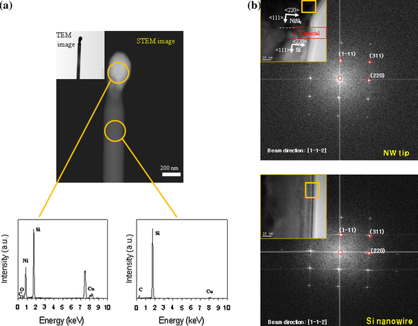
a Transmission electron microscopy (TEM) image of nanowire and its tip. Energy dispersive spectrometer (EDS) analysis shows that nanowire consists of silicon and that the tip of nanowire is mostly composed of silicon and nickel that was used as a catalyst during the chemical growth. b TEM image of silicon nanowire and its tip. TEM image shows that silicon nanowire is chemically grown in the (111) direction, and so does the tip of nanowire
For mechanical characterization of nanowires using AFM nanoindentation, we have utilized commercially available AFM (Innova, Santa Barbara, CA, USA) with Nanodrive controller (Veeco, Santa Barbara, CA, USA) and closed-loop scanner. For both imaging and indentation, we have used Al-coated silicon cantilevers (TESPA, Veeco, Santa Barbara, CA, USA) with their nominal tip radius of ~10 nm. The force constant of AFM cantilever is calibrated from Sader’s method [20] such that spring constant is directly computed from the measured resonant frequency of such a cantilever. In this study, we have employed the silicon cantilever whose calibrated force constant is 34.5 N/m, otherwise specified. AFM images of silicon nanowire is obtained from AFM tapping mode with a scanning rate of 0.6 Hz and scan size in the range of 20 μm × 20 μm to 500 nm × 500 nm. Figure 2 shows the AFM images of silicon nanowire and its cross-sectional view. For reliable indentation of nanowires using AFM, we have to insure that the sample is not rolled during the indentation. For such a reliable indentation, we have used “oscillation off” mode in Innova in order to turn off the cantilever’s oscillation in tapping state. Further, the precise probe positioning of AFM cantilever is attributed to the closed-loop system. The reliable manipulation of AFM cantilever due to “oscillation off” mode and precise probe positioning enable us to acquire the vivid image of silicon nanowire as well as the robust indentation response recorded in load–displacement curve. Here, we have applied a mechanical force until 800 nN with a loading rate of 35 nm/s in order to insure that the indentation response of nanowire resides in the linear elastic regime, which can be depicted by classical Hertz theory.
Figure 2.
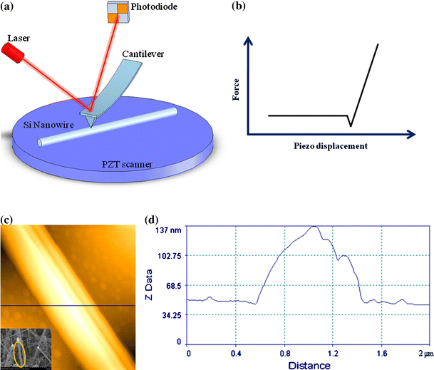
a Schematic illustration of atomic force microscopy (AFM) nanoindentation of silicon nanowires. Laser beam was used to measure the cantilever bending deflection (that can be converted to mechanical force exerted by AFM cantilever) during the nanoindentation. b Typical force-piezo displacement (F-z) curve for AFM indentation of nanowires. c The image of silicon nanowire is obtained from tapping-mode AFM. The inset shows the scanning electron microscopy (SEM) image of silicon nanowires chemically grown. d Topological profile for cross section of nanowire along the line shown in (c)
A typical force-piezo displacement curve (F-z curve) obtained from AFM nanoindentation of silicon nanowire is shown in Fig. 3. It should be noted that the F-z curve is independent of the indentation location where AFM cantilever is under contact with a nanowire. Specifically, as shown in Fig. 3, we have confirmed that F-z curves obtained from indentation at five different indentation locations are identical to each other. This indicates that mechanical response of a nanowire by nanoindentation does not depend on the indentation location on a nanowire. It should be recognized that the F-z curve does not directly provide the relation between mechanical force and indentation displacement, since the piezo displacement includes both AFM cantilever bending deflection and indentation displacement for a nanowire. Thus, because piezo displacement is equal to summation of AFM cantilever bending deflection and nanowire indentation displacement, we have a relation of [21,22]
Figure 3.
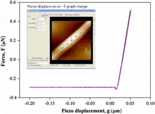
Force-piezo displacement (F-z) curves for five points in a silicon nanowire. It is shown that F-z curves are identical to each other, indicating that F-z curve is independent of position where AFM tip contacts during the indentation
where kAFM and kNW represent the force constants for AFM cantilever and silicon nanowire (for indentation), respectively. Here, the force constant of AFM is estimated as kAFM = 34. 5 N/m computed from Sader’s method. Figure 4 depicts the force constant of silicon nanowire with diameter of 525 nm obtained from AFM nanoindentation. It is shown that the force constant of nanowire depends on the applied force during indentation. In order to understand the relationship between force constant of nanowire, kNW, and applied force, F, we have employed the classical elasticity theory such as Hertz theory, which provides the relationship between applied force, F, and indentation displacement, s, such as [23]
Figure 4.
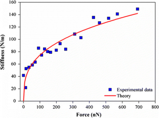
Stiffness of silicon nanowire, kNW, with its diameter of 525 nm as a function of indentation force, F. It is shown that the relationship between kNW and F is well described by a scaling of kNW = αF1/3, where α is a constant parameter depending on nanowire geometry. It implies that nanoindentation of silicon nanowire is well described by classical elasticity theory such as Hertz theory
Here, R is the AFM tip radius, and E* is the effective Young’s modulus defined as E* = [(1 − ν1)/E1 + (1 − ν2)/E2]−1, where Ei and νi indicate the Young’s modulus and the Poisson’s ratio for AFM tip (i = 1) or nanowire (i = 2), respectively. As a consequence, the force constant for nanowire as a function of mechanical force during an indentation is given by
This indicates that the relationship between force constant of nanowire during an indentation and applied force is well described by scaling law such as kNW = αF1/3. It should be noted that the scaling law for relationship between force constant of nanowire for nanoindentation and applied force is valid regardless of contact geometry (except the different coefficient α) [21]. As shown in Fig. 4, the experimental result showing the relation between nanowire’s stiffness and force is well dictated by Eq. (3). This implies that our nanoindentation experiments reside in the elastic regime as long as applied force is in the range of 0 <F < 1 μN.
We have considered the mechanical properties of silicon nanowires with various diameters in the range of ~80 to ~600 nm in order to understand the any role of finite size effect on the mechanical properties. From Hertz theory described in Eq. 3, we have extracted the Young’s modulus of silicon nanowires from the curves that show the relationship between force constant of nanowire and applied force (e.g., see Fig. 4). Figure 5 shows the Young’s modulus of various nanowires with respect to their diameters. It is found that the diameter of nanowire does not play any role on the mechanical properties of nanowire if its diameter is larger than ~100 nm. This indicates that, for nanowires with their diameter in the range of ~80 to ~600 nm, the Young’s modulus of nanowires is close to that of bulk silicon in the (111) direction. This is consistent with a recent study by Li and coworker [24], who showed that elastic modulus of amorphous silicon nanowire is independent of its diameter (in the range of ~80 to ~500 nm). Moreover, a recent study by Boland and coworkers [5,16] provides that the finite size effect may not play a significant role on the mechanical properties (e.g., elastic modulus) of nanowires. This is consistent with our finding that elastic modulus of our nanowires is unaffected by their sizes and that Young’s modulus of nanowires is close to that of bulk material. This implies that the elastic modulus of bulk material can be employed for design of nanomechanical devices using nanowires. However, it has to be reminded that the finite size effect does not appear since our nanowire has the diameter of >~80 nm. In a recent study by Li and coworkers [25], the finite size effect due to surface effect (e.g., surface stress effect) has played a vital role on elastic modulus of nanowire (e.g., ZnO nanowire) with its diameter of ~30 nm (≪100 nm). Specifically, for diameter less than ~30 nm, the surface effect such as surface stress reduces the elastic modulus of ZnO nanowire as its diameter is decreased [25]. In our case, the elastic modulus of silicon nanowire with its diameter of ~80 nm is smaller than that of bulk silicon. This may imply that elastic modulus of silicon nanowire may be reduced as its diameter is decreased [26]. It should be recognized that the dimension of our silicon nanowires is much larger than the critical dimension at which the surface effect does play an important role on elastic properties of nanowires. The role of surface effect on the elastic properties of nanowires with a diameter of ~20 nm will be considered for our future study.
Figure 5.
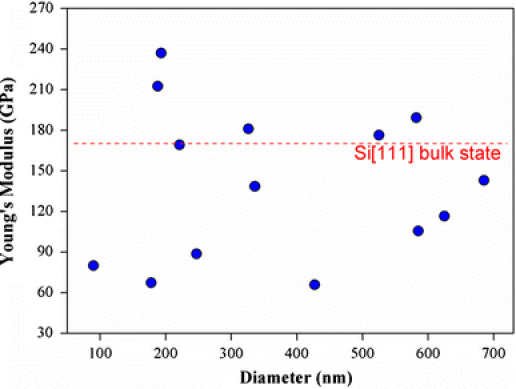
Young’s modulus of various silicon nanowires with their diameters in the range of ~100 to ~600 nm extracted from AFM indentation
In conclusion, we have demonstrated the AFM nanoindentation of nanowires for extracting their elastic modulus. Specifically, we have employed the classical elasticity theory (Hertz theory), which dictates the elastic response of silicon nanowires to AFM indentation. It is shown that Young’s modulus of silicon nanowires with their diameter of ~80 nm to ~600 nm is independent of their diameters, indicating that finite size effect due to surface effect does not play any role on elastic properties of nanowires. Moreover, the Young’s modulus of our nanowires with a diameter in the range of >~100 nm is close to that of bulk silicon. Therefore, the elastic modulus of bulk silicon can be assumed for design of nanomechanical devices using silicon nanowires with their diameters of >~100 nm.
Misc
Young-Soo Sohn and Jinsung Park equally contributed to this work.
Contributor Information
Taeyun Kwon, Email: tkwon@yonsei.ac.kr.
Kilho Eom, Email: kilhoeom@korea.ac.kr.
Acknowledgments
This work supported in part by Korea Science and Engineering Foundation (KOSEF) under Grant No. 2009-0071246 (to K.E.), Korea Research Foundation (KRF) under Grant No. KRF-2008-313-D00031 (to T.K.), Pioneer Research Center Program through National Research Foundation of Korea under Grant No. 2009-0082820 (to Y.-S.S., and J.-H.L.), and KOSEF under Grant No. R11-2007-028-03002 and Grant No. R01-2007-000-10497-0 (to S.N.).
References
- Chen CQ, Shi Y, Zhang YS, Zhu J, Yan YJ. Phys. 2006. p. 075505. COI number [1:STN:280:DC%2BD283gtFCqsg%3D%3D]; Bibcode number [2006PhRvL..96g5505C] [DOI] [PubMed]
- Baughman RH, Cui C, Zakhidov AA, Iqbal Z, Barisci JN, Spinks GM, Wallace GG, Mazzoldi A, De Rossi D, Rinzler AG, Jaschinski O, Roth S, Kertesz M. Science. 1999. p. 1340. COI number [1:CAS:528:DyaK1MXjs1Wjtb4%3D]; Bibcode number [1999Sci...284.1340B] [DOI] [PubMed]
- Lee C, Wei X, Kysar JW, Hone J. Science. 2008. p. 385. COI number [1:CAS:528:DC%2BD1cXosVOrs7k%3D]; Bibcode number [2008Sci...321..385L] [DOI] [PubMed]
- Ngo LT, Almecija D, Sader JE, Daly B, Petkov N, Holmes JD, Erts D, Boland JJ. Nano Lett. 2006. p. 2964. COI number [1:CAS:528:DC%2BD28Xht1Slsr3F]; Bibcode number [2006NanoL...6.2964N] [DOI] [PubMed]
- Wu B, Heidelberg A, Boland JJ. Nat. 2005. p. 525. COI number [1:CAS:528:DC%2BD2MXlvFOjurk%3D]; Bibcode number [2005NatMa...4..525W] [DOI] [PubMed]
- Husain A, Hone J, Postma HWC, Huang XMH, Drake T, Barbic M, Scherer A, Roukes ML. Appl. 2003. p. 1240. COI number [1:CAS:528:DC%2BD3sXmtFOksbw%3D]; Bibcode number [2003ApPhL..83.1240H] [DOI]
- Feng XL, He R, Yang P, Roukes ML. Nano Lett. 2007. p. 1953. COI number [1:CAS:528:DC%2BD2sXmslGjtb0%3D]; Bibcode number [2007NanoL...7.1953F] [DOI]
- Jensen K, Girit C, Mickelson W, Zettl A. Phys. 2006. p. 215503. COI number [1:STN:280:DC%2BD28zptVyisw%3D%3D]; Bibcode number [2006PhRvL..96u5503J] [DOI] [PubMed]
- Bunch JS, van der Zande AM, Verbridge SS, Frank IW, Tanenbaum DM, Parpia JM, Craighead HG, McEuen PL. Science. 2007. p. 490. COI number [1:CAS:528:DC%2BD2sXotFCjtw%3D%3D]; Bibcode number [2007Sci...315..490B] [DOI] [PubMed]
- Yang YT, Callegari C, Feng XL, Ekinci KL, Roukes ML. Nano Lett. 2006. p. 583. COI number [1:CAS:528:DC%2BD28Xit1OrsLg%3D]; Bibcode number [2006NanoL...6..583Y] [DOI] [PubMed]
- Eom K, Kwon TY, Yoon DS, Lee HL, Kim TS. Phys. Rev. B. 2007. p. 113408. Bibcode number [2007PhRvB..76k3408E] [DOI]
- Jensen K, Kim K, Zettl A. Nat. 2008. p. 533. COI number [1:CAS:528:DC%2BD1cXhtVOqsLrL] [DOI] [PubMed]
- Zheng M, Eom K, Ke C. J. 2009. p. 145408. Bibcode number [2009JPhD...42n5408Z] [DOI]
- He R, Yang P. Nat. 2006. p. 42. COI number [1:CAS:528:DC%2BD28XhtFCisrrJ]; Bibcode number [2006NatNa...1...42H] [DOI] [PubMed]
- Heidelberg A, Ngo LT, Wu B, Phillips MA, Sharma S, Kamins TI, Sader JE, Boland JJ. Nano. 2006. p. 1101. COI number [1:CAS:528:DC%2BD28XksFWiu70%3D]; Bibcode number [2006NanoL...6.1101H] [DOI] [PubMed]
- Wen B, Sader JE, Boland JJ. Phys. 2008. p. 175502. Bibcode number [2008PhRvL.101q5502W] [DOI] [PubMed]
- He J, Lilley CM. Nano Lett. 2008. p. 1798. COI number [1:CAS:528:DC%2BD1cXmsVKhur4%3D]; Bibcode number [2008NanoL...8.1798H] [DOI] [PubMed]
- Peng B, Locascio M, Zapol P, Li S, Mielke SL, Schatz GC, Espinosa HD. Nat. 2008. p. 626. COI number [1:CAS:528:DC%2BD1cXht1SlurjO] [DOI] [PubMed]
- Zhao MH, Ye Z-Z, Mao SX. Phys. 2009. p. 045502. COI number [1:STN:280:DC%2BD1M7ot12qsA%3D%3D]; Bibcode number [2009PhRvL.102d5502Z] [DOI] [PubMed]
- Sader JE, Chon JWM, Mulvaney P. Rev. 1999. p. 3967. COI number [1:CAS:528:DyaK1MXmt1yhtr4%3D]; Bibcode number [1999RScI...70.3967S] [DOI]
- Palaci I, Fedrigo S, Brune H, Klinke C, Chen M, Riedo E. Phys. 2005. p. 175502. COI number [1:STN:280:DC%2BD2MzgsV2rtQ%3D%3D]; Bibcode number [2005PhRvL..94q5502P] [DOI] [PubMed]
- Lucas M, Mai W, Yang R, Wang ZL, Riedo E. Nano Lett. 2007. p. 1314. COI number [1:CAS:528:DC%2BD2sXktlChsLc%3D]; Bibcode number [2007NanoL...7.1314L] [DOI] [PubMed]
- Johnson KL. Contact Mechanics. Cambridge University Press, Cambridge; 1987. [Google Scholar]
- Ni H, Li X, Gao H. Appl. 2006. p. 043108. Bibcode number [2006ApPhL..88d3108N] [DOI]
- Wang G, Li X. Appl. 2007. p. 231912. Bibcode number [2007ApPhL..91w1912W] [DOI]
- Zhu Y, Xu F, Qin Q, Fung WY, Lu W. Nano Lett. 2009. [DOI] [PubMed]


