Abstract
Nanostructured silver films have been prepared by thermal deposition on silicon, and their properties as SERS substrates investigated. The optimal conditions of the post-growth annealing of the substrates were established. Atomic force microscopy study revealed that the silver films with relatively dense and homogeneous arrays of 60–80-nm high pyramidal nanoislands are the most efficient for SERS of both organic dye and inorganic nanoparticles analytes. The noticeable enhancement of the Raman signal from colloidal nanoparticles with the help of silver island films is reported for the first time.
Keywords: SERS, Ag/Si nanoisland films, Post-growth annealing, Rhodamine 6G, CdSe, Nanoparticles
Introduction
The field of physical and chemical phenomena related to the interaction of molecules and other nanoobjects with plasmons localized in or propagating over specially designed noble metal nanostructures has received increasing interest in recent years [1-8]. The great progress achieved in both the technology of metal nanostructures with necessary parameters and in theoretical modelling of many particular problems has led to a broad involvement of plasmon-mediated phenomena in the fields of optoelectronics, medical diagnostics and treatment, sensor technologies, etc. [5,7]. Among these phenomena surface-enhanced Raman scattering (SERS) and photoluminescence are believed to have great perspectives in single-molecule chemical and bio-sensing and in vivo medical diagnostics [5,6].
Surface enhanced Raman scattering (SERS) has proven to be one of the most powerful analytical tools. This phenomenon represents strong increase of the Raman signal from analyte molecules deposited on nanostructured metallic surface.
There are two main mechanisms of SERS, long-range electromagnetic effect and short-range chemical effect. The part of electromagnetic mechanism in the resulting intensity is dominating (about 104–107), while chemical mechanism contributes only about 10–102[1]. Chemical mechanism acts only for the first layer of analyte in direct contact with metallic surface, when charge transfer between surface and adsorbate molecule can occur. Electromagnetic mechanism is caused by electric field enhancement by excitation of surface plasmon resonance in proximity with nanoscale roughness [2].
One of the main prerequisites for a wide range of applications of surface enhanced spectroscopy is the availability of non-expensive nanostructured metal substrates with a morphology optimized for a maximum enhancement. The main approaches towards the preparation of such substrates are colloidal synthesis, use of templates, etching, and self-assembled formation of rough (island-like) metal surfaces [8]. Colloidal metal nanoparticles (NPs) are relatively inexpensive, and a narrow size dispersion of NPs can be obtained, which allows spectrally narrow plasmon peaks to be obtained [8]. While even better homogeneity of the nanostructures and related plasmon characteristics can be achieved by etching and using templates, these kinds of methods are more expensive. Self-assembled growth of island metal films on dielectric or semiconductor substrates can be a good candidate for obtaining SERS substrates with an acceptable ratio of price/quality, provided that the necessary homogeneity of the island size is achieved [5,9-11]. Furthermore, investigations of the SERS effect on various kinds of metal nanostructures and analyte will contribute to the understanding of the role of electromagnetic and chemical contributions to this effect—an issue intensively discussed due to both application importance and fundamental interest [12,13].
Here, we report a study of the relation between the preparation conditions of island-like silver substrates, their morphology, and SERS properties. Rhodamine 6G (Rh6G) was chosen as an analyte due to its broad application as fluorescent labelling and sensing reagent [14,15], as well as due to its common use as an analyte in testing SERS substrates [16]. In addition, the SERS spectra of the nanoparticles of an inorganic semiconductor, CdSe, are also obtained and analysed. In contrast to the huge work done on SERS experiments with molecules as analyte [1-3], only a few attempts succeeded in observing surface enhancement of Raman signal from semiconductor nanoparticles as analyte [17-23]. At the same time, the effect of interaction with the plasmon onto the optical and electrical properties of semiconductor NPs is presently an intense field of research [24]. The reported successful SERS experiments on semiconductor NPs were realized using colloidal Ag NPs [17,21,22], Ag–CdS composites formed by the Langmuir–Blodgett technique [23], or by thermal deposition of silver onto the epitaxialy grown nanostructures [19,20]. In the present work, SERS of colloidal semiconductor NPs deposited on silver island film is reported for the first time.
Experimental
The initial Ag/Si nanoisland film was prepared by thermal evaporation of silver onto a cleaned silicon substrate at room temperature. The nominal thickness of the silver deposited was adjusted to (10 ± 2) nm, as estimated from the known time and rate of deposition. A series of the samples was produced by annealing of the initial Ag/Si films under ambient or nitrogen atmosphere. The actual dimensions of both the initial surface roughness and of the islands obtained after thermal treatment were derived from atomic force microscopy (AFM) images of the surface. AFM images were taken using a NanoScope IIIa set-up (Digital Instruments) operating in the tapping mode. The SERS experiments were performed using Rhodamine 6G, Cu porphyrin CuTMPy, or colloidal CdSe nanoparticles as analytes. Raman spectra of the samples were excited with the 514.5-nm line of an Ar+ion laser with a power on sample of 5 mW and registered with using a Renishaw Ramascope 2000.
The synthesis of CdSe and CdSe/ZnS NPs was undertaken following a modified procedure of Peng et al. [25]. Cadmium oxide (CdO, 99.5%), 1-octadecene (ODE), oleic acid (OA), trioctylphosphine oxide (TOPO, 99%), Zinc acetate (ZnAc2, 99.99%), Sulphur powder (S, 99.98%) and all organic solvents were purchased from Aldrich. Hexadecylamine (HDA, >99%), octadecylamine (ODA, >90%) and n-trioctylphosphine (TOP) were obtained from Fluka and Selenium powder (Se, 99.99%) was purchased from ChemPur. All chemicals were used without further treatment, except TOP which was purified by distillation. In a typical synthesis of CdSe nanocrystals, a mixture of 0.4 mmol of CdO, 2 mmol of OA in 9.5 g of ODE was heated to 100°C under vacuum for 30 min to remove any residual oxygen and moisture. Under inert (Ar) atmosphere, this mixture was further heated to 300°C until a clear, colourless solution was obtained. After cooling this solution to 100°C, 5 mmol of TOP and 8 mmol of HDA were added and the resulting mixture was kept at 100°C under vacuum for 30 min. After heating to 270°C under inert atmosphere, a mixture of 0.4 mmol of Se in 4.5 mmol TOP and 1.5 g ODE was swiftly injected and the solution temperature held at 245°C until the desired particle size was obtained. The resulting particles were then purified by precipitation with an iso-propanol/methanol mix and redissolved in hexane or toluene.
The shell growth was carried out using the SILAR technique [25]. An aliquot containing 10−4 mmol of CdSe nanocrystals in hexane was combined with 1.5 g of ODA and 5.0 g of ODE and heated to 100°C under vacuum for 30 min to remove any residual oxygen and moisture. Subsequently the system was switched to inert atmosphere and heated to 240°C for the shell growth. The shell growth was achieved by a series of alternating injections of a solution of ZnAc2/OA/ODE (0.04 M, OA:ODE = 1:3) and S/ODE (0.04 M). The purification steps for the core/shell nanoparticles were as previously described for the uncoated CdSe nanocrystals.
Results and Discussion
The growth of silver on silicon is known to follow the Stranski–Krastanov mechanism, i.e. formation of a continuous Ag wetting layer with three-dimensional pyramid-like islands on it. However, with annealing at high temperatures Tann in the range of 300–600°C, the interaction energy between silver atoms becomes stronger than the interaction energy between silver and silicon substrate and ripening of 3D silver islands is enhanced.
The AFM image of the surface of the initial Ag/Si sample studied in the present work is shown in Fig. 1a. As one can see, the surface roughness is quite inhomogeneous, with an average height of the islands of about 1 nm. After 15 min of thermal annealing of the film at 550°C under air atmosphere, a quite dense array of islands is formed, with the island height increased up to (70 ± 10) nm (Fig. 1b). As the annealing time,tann, goes up to 30 min, the reverse process of islands collapsing takes place and their number per surface area unit and average height increases at the expense of the mean island size decrease. Already for tann = 30 min, the surface morphology becomes again close to the initial (not annealed) film (Fig. 1c).
Figure 1.
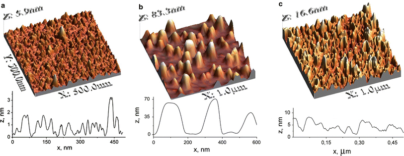
AFM images and corresponding surface profiles of Ag/Si nanoisland films: unannealed film a and films annealed in air at 550°C for b 15 and c 30 min
The measurements of the Raman spectra of 10−5M Rhodamine 6G, deposited onto the surface of the Ag island films, revealed that the enhancement factor is strongly dependent on the morphology of the film and determined by annealing time. In particular, for the Tann = 550°C, the optimum parameters of the island film are achieved at the tann = 15–20 min (Fig. 2). Therefore, it can be concluded from comparison of the morphology and SERS spectra that for the maximum enhancement rather dense arrays of islands with size of ten to several tens of nm are preferable (Fig. 1). At that, the intensity of Raman features for samples with rather different island morphology, corresponding to 15 and 30 min of annealing, is rather comparable, while the substrates with more similar morphologies, corresponding to the initial film and that annealed for 30 min, reveal drastic difference of the enhancement properties (Fig. 2). To explain this fact, we assume that along with the apparent morphology (seen in AFM-images) other factors can play a significant role in determining the enhancement factor. One of such factors can be different thickness of the silver oxide layer on the surface of the films. In particular, the surface of the initial films is supposed to have a negligible (thinnest) oxide layer. Its surface is more likely covered with silver sulphide due to the reaction between silver and H2S from air during the storage of the films under air. The sulphide film can probably be removed during the high-temperature annealing. Instead, silver oxide forms, which positively influences the enhancement property of the island film, with the oxide thickness increasing with tann. We return to this discussion at the end of the manuscript.
Figure 2.
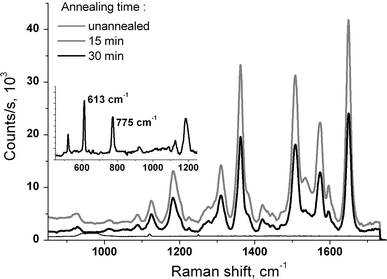
Raman spectra of 10−5M Rh6G on Ag/Si nanoisland films annealed at 550°C and different annealing times. Inset shows the lower frequency peaks at 613 and 775 cm−1
Based on a relatively strong intensity of the peaks at 613 and 775 cm−1, which are markers for charge transfer (chemical) component of the SERS on Rh6G (Fig. 2, inset) [26], we can conclude that the chemical mechanism also contributes to the enhancement in our case.
The annealing temperature is another crucial factor governing the Ag/Si films surface morphology. The increase of Tann increases the average height of nanoislands (Fig. 3) and this improves enhancing characteristics of such substrates, up to Tann of about 550°C. The highest SERS efficiency is produced by substrates annealed at temperatures 500–550°C. The reason is probably that closely positioned nanoislands of appropriate size (height of 70 ± 10 nm) and relatively large surface density are formed, as can be seen from the corresponding AFM image (Fig. 3c). At increase of the annealing temperature above 600°C, “melting” and “merging” of islands occur (Fig. 3d) and their SERS activity deteriorates. The Raman signal surface enhancement level of the sample annealed at 610°C is about 15 times weaker than that of the sample annealed at 550°C. At the same time, the enhancement factor achieved with the Ag/Si film annealed at 550°C is two orders of magnitude larger than for 350°C (Fig. 4). The absolute enhancement for the substrate annealed at 550°C is at least three orders of magnitude, but the exact value was not possible to be derived from the present experiments. The reason is that no Raman signal could be registered from the given concentration of analyte deposited on the initial (not annealed) Ag film.
Figure 3.
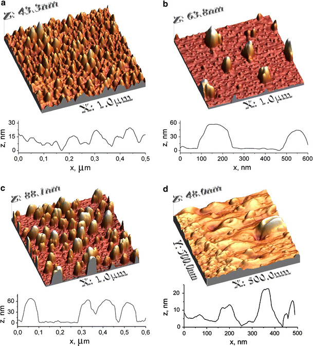
AFM images and corresponding surface profiles of Ag/Si nanoisland films annealed in air during 15 min at a 350°C, b 420°C, c 550°C and d 650°C
Figure 4.
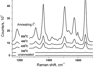
Raman spectra of 10−5M Rh6G measured on Ag/Si nanoisland films, obtained by annealing at different temperatures for 15 min
Special attention in the present work was paid to the stability of the prepared SERS substrates to environment during long storage or multiple use. It was found that the enhancement factor of the Ag/Si substrates does not change significantly after storage for months under ambient atmosphere. For example, the spectra shown in Figs. 2 and 4 were taken from freshly deposited analyte on Ag/Si nanoisland films after a 5-month storage. This clearly indicates the stability of the surface morphology of such nanostructured films. Probably, one of the factors which provide such stability is the (thin) layer of silver oxide formed during annealing in air. The presence of such oxide layer was revealed in the Raman spectra and will be discussed in the following paragraphs. Moreover, the role of the oxide in the SERS activity of such substrates is further confirmed by the fact that the substrates annealed in inert (nitrogen) atmosphere did not possess noticeable SERS activity.
We also investigated the stability of the substrates prepared with respect to multiple use for one and the same analyte, as well as for different analyte. Immediately after deposition of an analyte and its spectra registration, the nanoisland films were kept and rinsed in ethanol for 1 h and then another analyte was deposited on them again and the next measurements were carried out. The subsequent measurements gave Raman signals of the same order of magnitude.
The Raman spectra of CuTMPy of different concentration were also studied. The maximum enhancement was achieved for Ag/Si nanoisland films obtained at Tann = 500–550°C (Fig. 5), similarly to the Rh6G analyte. One of the main Raman bands of CuTMPy was registered at concentrations down to 10−6M.
Figure 5.
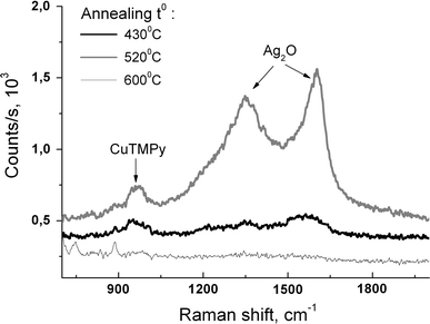
Raman spectra of 10−6M CuTMPy measured on Ag/Si nanoisland films, annealing time 15 min
At low signal intensities from the analyte molecule, like in Fig. 5, we could observe two additional features centred near 1,350 and 1,600 cm−1, correspondingly. These features can be attributed to scattering by vibrational modes of silver oxide, Ag2O [27], formed on the surface of the island film during high-temperature annealing. Interestingly, these two Raman peaks change in intensity almost synchronously with the analyte peak (Fig. 5). We believe that the Ag2O vibrations also undergo surface enhancement and the variation of their intensity with temperature of the Ag layer annealing is not a result of different Ag2O volume. If the latter were the case, we would expect an increase of the Ag2O-related Raman signal for the substrate obtained at 600°C (Fig. 5). Instead we observe negligible peak intensity for this Tann, which correlates with the low intensity of the analyte peak and indicates an enhancement for both features via the SERS effect.
Growing fundamental and applied interest in manipulating the optical and electronic properties of semiconductor NPs by plasmon fields generated in adjacent nanostructured metal has been observed in recent years [3-7]. In view of this interest, we investigated the SERS effect on colloidal CdSe NPs. Two kinds of NPs were investigated. The NPs of the first kind were homogenous (bare) CdSe NPs capped by organic ligands to preclude their aggregation. The CdSe NPs of the second kind were core-shell systems consisting of a CdSe core capped with a thin ZnS shell. The diameter of the core was about 3 nm, the shell thickness was approximately 0.5–1 nm. The diameter of the CdSe core was determined from the spectral position of the first absorption maximum, based on the relations derived in [16].
Unlike the spectrum of the control sample with the same concentration of NPs deposited on glass, bare silicon or the unannealed (initial) Ag film, the surface enhancement effect induced by the Ag nanoisland film allowed for both CdSe and CdSe/ZnS NPs the Raman bands attributed to the longitudinal optical (LO) phonon of CdSe core at 203 cm−1 and its overtone (2LO) near 400 cm−1 to be recorded (Fig. 6). The largest Raman signal enhancement was observed for Ag/Si substrates annealed at temperatures 400–500°C, which differ from the temperatures optimal for the case discussed earlier of molecular analyte, R6G (500–550°C).
Figure 6.
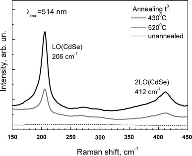
Raman spectra of CdSe/ZnS NPs on unannealed Ag/Si substrates and nanoisland films formed by annealing for 15 min at 430 and 520°C
As SERS is known to be a short-range effect due to the drastic drop of the plasmon field magnitude at distances of several nanometer from the metal surface [3], one might expect the predominant enhancement of the Raman peaks corresponding to the atomic vibration on the surface or in the near-surface region of the NP. This assumption is in agreement with the results of Ref. [21] where an SERS signal was obtained from the thin CdS shell of the surface of CdTe/CdS NPs, while no signal from the CdTe core was registered. In the present study, we did not observe the Raman peak related to the ZnS shell, expected around 350 cm−1, neither in the ordinary nor in the SERS spectrum (Fig. 7). The fact that the Zn–S vibrational mode is commonly not possible to register in an ordinary Raman scattering measurement on CdSe/ZnS NPs [28,29] can be easily explained by the off-resonance conditions of the visible laser excitations with the electronic transitions in the ZnS shell. Instead we observe in both spectra the feature ~270–280 cm−1, previously assigned to the Cd–S vibrations at the intermixed core-shell interface [28,29]. The intensity of this Cd–S mode is very close in both (normalized) spectra (Fig. 7). This fact indicates that the enhancement of this mode is the same as for the core-related LO phonon. The absence of the shell-related peak, as well as the fact that the optimum annealing temperature (and therefore the Ag film morphology and its plasmon parameters) differs for SERS of Rh6G and semiconductor NPs indicate that the resonant excitation of the plasmon alone is not enough to cause the SERS effect of the semiconductor NPs. The excitation wavelength should also be resonant with certain electronic transition of the NP (either core or shell), for the corresponding vibrations to be observed in the resonant Raman spectra. This case of double resonance takes place for the exciton (e-h) transitions of the CdSe core, as the excitation energy used (2.4 eV) is well above the absorption onset of the NPs (1.9 eV). On the contrary, no resonance is realized at these conditions for the electronic transition of the thin ZnS shell, because the bandgap is as large as 3.6 eV for bulk ZnS crystal [30] and is equal to and can reach more than 4.3 eV in the very thin (sub-nm) layer due to quantum confinement effect [31].
Figure 7.
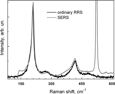
Normalized Raman spectra of the same NPs sample with plasmon enhancement (grey) and without it (black). The SERS spectrum is same as in Fig. 6 for Tann = 430°C. The ordinary spectrum was obtained by deposition of NPs from a highly concentrated solution onto the bare Si surface
One of the inherent (i.e. not from the shell) surface-related vibrational modes reported for semiconductor NPs, which might be expected to be enhanced in SERS spectrum, is the so-called surface optical (SO) phonon [32-34]. The frequency of the SO mode is usually 15–25 cm−1 below that of the corresponding longitudinal optical (LO) phonon related to the internal (bulk-like) undistorted part of the NPs. The SO mode is usually observed as a more or less distinct shoulder on the lower frequency side of the LO peak (Fig. 7) [32-34]. By comparing the lineshape of the SERS and the ordinary spectra in the region of SO and LO modes (Fig. 7), we can conclude that the enhancement is of the same magnitude for LO and SO modes. Our results qualitatively agree with those obtained in Refs. [17,18,23]. The latter results may indicate that the enhancement of Raman scattering by (bulk-like) LO phonons occurs via enhanced absorption of the exciting light in NPs, mediated by the plasmon excitation. Therefore, the SERS effect in this case occurs not locally but for the NPs as a whole. This fact can be an indication of the spatial extension of the plasmon enhancement being noticeable even at the distance of several nm from the metal surface, in accordance with Otto etal. [35,36]. The concentration of the exciting light energy near the apex of silver nanoislands of special morphology leads to the generation of a larger number of excitons (electron-hole pairs) inside the adjacent semiconductor NPs. The latter means a larger number of the phonon scattering events. The probability of the scattering on the strength of the electron- (exciton-) phonon coupling (EPC) may thus be the same as in the ordinary (resonant) RS. The value of the EPC strength can be estimated from the intensity ratio of the LO peak and its overtone (near 415 cm−1) [29], and this value is very close in both the SERS and RRS spectra (Fig. 7).
Conclusions
We have studied the dependence of the SERS efficiency of nanostructured silver films, prepared by thermal deposition on silicon, on the parameters of their post-growth annealing. It was found that the annealing under ambient but not inert atmosphere gives the remarkable enhancement factor. The optimal conditions of a post-growth annealing of the substrates have been established to be Tann = 400–550°C and duration of 15–20 min. Atomic force microscopy study revealed the relatively dense and homogenous array of 60–80-nm high pyramidal nanoislands, formed at such annealing conditions, to be most efficient for SERS of both organic dye and inorganic nanoparticles analyte. The noticeable enhancement of the Raman signal from colloidal semiconductor nanoparticles with help of silver island films is reported for the first time (in opposite to using of colloidal Ag in [21] or Langmuir–Blodgett technique in [20]).
Acknowledgments
Authors are grateful to D. Cojoc from CNR-INFM, Laboratorio Nazionale TASC, Area Science Park—Basovizza, Trieste, Italy for the help with carring out Raman spectra measurements and useful advice. V. Dzhagan is grateful to the Alexander von Humboldt Foundation for financial support of his work.
Open Access
This article is distributed under the terms of the Creative Commons Attribution Noncommercial License which permits any noncommercial use, distribution, and reproduction in any medium, provided the original author(s) and source are credited.
References
- Tripp RA, Dluhy RA, Zhao Y. Nanotoday. 2008. p. 31. COI number [1:CAS:528:DC%2BD1cXhtFemsbjN]
- Lu Z, Gu Y, Yang J, Li Z, Ruan W, Xu W, Zhao C, Zhao B. Vib. 2008. p. 99. COI number [1:CAS:528:DC%2BD1cXmvFOmu74%3D] [DOI]
- Kneipp K, Moskovits M, Kneipp H, editor. Surface-Enhanced Raman Scattering: Physics and Applications. Springer, Belin; 2006. [Google Scholar]
- Lakowicz JR, Ray K, Chowdhury M, Szmacinski H, Fu Y, Zhang J, Nowaczyk K. Analyst. 2008. p. 1308. COI number [1:CAS:528:DC%2BD1cXhtFemsrjE]; Bibcode number [2008Ana...133.1308L] [DOI] [PMC free article] [PubMed]
- Culha M, Stokes D, Allain LR, Vo-Dinh T. Anal. 2003. pp. 22–6196. [DOI] [PubMed]
- Qian X-M, Nie SM. Chem. 2008. p. 912. COI number [1:CAS:528:DC%2BD1cXltFOksbs%3D] [DOI] [PubMed]
- Smith WE. Chem. 2008. p. 955. COI number [1:CAS:528:DC%2BD1cXltFOksbk%3D] [DOI] [PubMed]
- Schwartzberg AM, Zhang JZ. J. Phys. Chem. C. 2008. p. 10323. COI number [1:CAS:528:DC%2BD1cXmvVWrurs%3D] [DOI]
- Ito Y, Matsuda K. and Y. Kanemitsu Phys. Rev.B. 2007. p. 033309. Bibcode number [2007PhRvB..75c3309I] [DOI]
- Lu G, Shen H, Cheng B, Chen Z, Marquette CA, Blum LJ, Tillement O, Roux S, Ledoux G, Ou M, Perriat P. Appl. 2006. p. 223128. Bibcode number [2006ApPhL..89v3128L] [DOI]
- Li PW, Zhang J, Zhang L, Mo YJ. Vib. 2009. p. 2. COI number [1:CAS:528:DC%2BD1cXhsFahtbvL] [DOI]
- Sun M, Wan S, Liu Y, Jia Y. Hongxing Xu, J. 2008. p. 402. COI number [1:CAS:528:DC%2BD1cXkt1yqtLw%3D]; Bibcode number [2008JRSp...39..402S] [DOI]
- Moskovits M. Rev. 1985. p. 783. COI number [1:CAS:528:DyaL28Xkt1Smsw%3D%3D]; Bibcode number [1985RvMP...57..783M] [DOI]
- Shiraishi Y, Sumiya S, Kohno Y, Hirai T. J. 2008. p. 8571. COI number [1:CAS:528:DC%2BD1cXht1SjtLrJ] [DOI] [PubMed]
- Lakowicz JR. Principles of Fluorescence Spectroscopy. Springer, New York; 2006. [Google Scholar]
- Yu WW, Wang YA, Peng X. Chem. 2003. p. 4300. COI number [1:CAS:528:DC%2BD3sXnslaltbs%3D] [DOI]
- Shan G, Wang S, Fei X, Liu Y, Yang G. J. Phys. Chem. B. 2009. p. 1468. COI number [1:CAS:528:DC%2BD1MXksVyrtw%3D%3D] [DOI] [PubMed]
- Kawai M, Yamamoto A, Matsuura N, Kanemitsu Y. Phys. Rev.B. 2008. p. 153308. Bibcode number [2008PhRvB..78o3308K] [DOI]
- Bessolov VN, Konenkova EV, Zhilyaev YV, Paez Sierra BA, Zahn DRT. Applied Surface Science. 2004. p. 274. COI number [1:CAS:528:DC%2BD2cXmvVOlu70%3D]; Bibcode number [2004ApSS..235..274B] [DOI]
- Milekhin AG, Meijers R, Richter T, Calarco R, Luth H, Paez Sierra BA, Zahn DRT. Phys. Stat. Sol. C. 2006. p. 2065. COI number [1:CAS:528:DC%2BD28XmvFOqur0%3D] [DOI] [PubMed]
- Wang Y, Li M, Jia H, Song W, Han X, Zhang J, Yang B, Xu W, Zhao B. Spectrochimica Acta Part A. 2006. p. 101. [DOI] [PubMed]
- Honma I, Sano T, Komiyama H. J. 1993. p. 6692. COI number [1:CAS:528:DyaK3sXktlKnu7o%3D] [DOI]
- Milekhin AG, Sveshnikova LL, Duda TA, Surovtsev NV, Adichtchev SV, Zahn DRT. JETP Letters. 2008. p. 799. COI number [1:CAS:528:DC%2BD1MXjt1eksrY%3D]; Bibcode number [2008JETPL..88..799M] [DOI]
- Rogach A, editor. Semiconductor Nanocrystal Quantum Dots: Synthesis, Assembly, Spectroscopy and Applications. Springer-Verlag, GmbH; 2008. [Google Scholar]
- Li JJ, Wang A, Guo W, Keay JC, Mishima TD, Johnson MB, Peng X. J. 2003. pp. 41–12567. [DOI] [PubMed]
- Hildebrandt P, Stockburger M. J. 1984. p. 5935. COI number [1:CAS:528:DyaL2cXmtFyrsr8%3D] [DOI]
- Chuang C-M, Wu M-C, Su W-F, Cheng K-C, Chen Y-F. Appl. 2006. p. 061912. Bibcode number [2006ApPhL..89f1912C] [DOI]
- Dzhagan VM, Valakh MY, Raevskaya AE, Stroyuk AL, Kuchmiy SY, Zahn DRT. Nanotechnology. 2007. p. 285701. [DOI] [PubMed]
- Dzhagan VM, Valakh MY, Raevska OE, Stroyuk OL, Kuchmiy SY, Zahn DRT. Nanotechnology. 2009. p. 365704. COI number [1:STN:280:DC%2BD1MrmtFCqtA%3D%3D] [DOI] [PubMed]
- Madelung O, Rössler U, Schulz M, Landolt-Bornstein , editor. Physics of II-VI and I-VII Compounds, Semimagnetic Semiconductors, New Series, Group III. Springer, Berlin; 1982. [Google Scholar]
- Li L, Pradhan N, Wang Y, Peng X. Nano Lett. 2004. p. 2261. COI number [1:CAS:528:DC%2BD2cXotlKks78%3D]; Bibcode number [2004NanoL...4.2261L] [DOI]
- Ingale A, Rustagi KC. Phys Rev B. 1998. p. 7197. COI number [1:CAS:528:DyaK1cXmtVamsLg%3D]; Bibcode number [1998PhRvB..58.7197I] [DOI]
- Azhniuk YM, Milekhin AG, Gomonnai AV, Lopushansky VV, Yukhymchuk VO, Schulze S, Zenkevich EI, Zahn DRT. J. Phys.: Condens. Matter. 2004;16:9069. COI number [1:CAS:528:DC%2BD2MXjtVemsA%3D%3D] [Google Scholar]
- Dzhagan VM, Valakh MY, Raevskaya AE, Stroyuk AL, Kuchmiy SY, Zahn DRT. Nanotechnology. 2008. p. 305707. [DOI] [PubMed]
- Otto A, Mrozek I, Grabhorn H, Akemann W. J Phys Condens Matter. 1992. p. 1143. COI number [1:CAS:528:DyaK38XhtFGqtro%3D]; Bibcode number [1992JPCM....4.1143O] [DOI]
- Otto A. In: in Topics in Applied Physics. M. Candona,G. Guntherodt, editor. Vol. 54. Springer, Berlin; 1984. pp. 289–418. [Google Scholar]


