Abstract
Porous anodic alumina (PAA) has been intensively studied in past decade due to its applications for fabricating nanostructured materials. Since PAA’s pore diameter, thickness and shape vary too much, a systematical study on the methods of morphology characterization is meaningful and essential for its proper development and utilization. In this paper, we present detailed AFM, SEM and TEM studies on PAA and its evolvements with abundant microstructures, and discuss the advantages and disadvantages of each method. The sample preparation, testing skills and morphology analysis are discussed, especially on the differentiation during characterizing complex cross-sections and ultrasmall nanopores. The versatility of PAAs is also demonstrated by the diversity of PAAs’ microstructure.
Keywords: Microscopy, Nanostructure, Porous, Anodic Alumina, Characterization
Introduction
Porous anodic alumina (PAA) has been discovered and applied in many industrial areas for more than a century. Due to its highly ordered hexagonal nanopore array and its wide applications for fabricating various nanostructured materials [1-3], the research on PAA has been very active during the past decade. The current PAA studies focus on the improvement of regulation, better controlling on pore diameter, interpore distance and thickness, high-speed growth, new types of pore structures [4-7], as well as its new applications [8,9]. These studies were mainly characterized by atomic force microscopy (AFM) [10,11], field emission scanning electron microscopy (FESEM) [12,13] and transmission electron microscopy (TEM) [14,15], and each characterizing method has its own advantages and disadvantages.
Generally, AFM can be only used to observe the PAA surface, and it has the advantage of no requirement on the conductivity of samples, and it also has the capability for characterizing PAAs with smaller nanopores. FESEM is widely used to observe the surface and cross-sections, and measure the thickness of different samples. We can use FESEM to fast relocate and obverse the desired sample area within several tens of nanometers to hundreds of micrometers, but the samples must have good electrical conductivity. Poor electrical conductivity will lead to blurry photos, unacceptable brightness variation and even characterization failure. Sometimes, in order to obtain better electrical conductivity, the conductive layers sputtered on samples may be so thick or the grain size is so large that the sputtered grains influence and even cover the true microstructure of PAA. TEM can be used to observe the cross-sections by slicing and thinning the sample, and observe the surface morphology by controlling the thickness of the sample within 100 nm. TEM also can be used to characterize PAAs’ composition and crystalline structure. But the pretreatments on samples are complicated and time-consuming, so AFM and FESEM are the most commonly used methods for observing PAAs’ microstructure.
However, PAA and its evolvements vary too much in microstructures, as well as in its application requirements as nanoscale templates. The pore diameter (10–500 nm), thickness (50–200 um), interpore distance (20–1,000 nm) and other structure parameters of PAAs can be continuously adjusted over a wide range, and the nanopore shapes can be circular, diamond/diamond-triangle [16] and square [17] by the aid of mold-pressing or lithography techniques. And the ordered nanopore array can transform into nanowires, nanotips, nanorods, nanosteps by post-treatments or tuning the anodizing process [18-20]. All of these different characteristics of PAA surfaces and sections require different techniques and skills of AFM, FESEM and TEM, but a systematical study on these characterizations has not been reported so far.
We already have a lot of experiences and good results on fabricating various PAA templates and their applications for fabricating nanostructure materials [20-24]. During our past works, we have accumulated some experiences and skills of characterizing different PAAs. In this paper, we have detailed AFM, FESEM and TEM studies on PAAs and their evolvements with different microstructures, and discuss the advantages and disadvantages of these methods. The structures of PAAs in this research include the regular PAA structures with different pore diameters, nanowires, nanotips and microstep-nanopore hierarchical structure. In particular, we discuss the characterization of PAAs’ unique fracture behaviors and complicated multilayer structures, PAAs with ultrasmall nanopores and the PAAs’ electrical conductivity. These works provide the techniques and skills for observing and identifying the special structures of all kinds of PAAs to the researchers.
Experimentals
High purity (99.999%) aluminum foils with the thickness of 200 μm were employed for fabricating PAAs. The as-rolled foils were immersed in acetone for few minutes and then washed in deionized water without further electrochemical polishing or thermal treatment. The regular PAA templates with different diameters and thickness were obtained in different electrolytes at different applied voltages and anodizing durations. PAAs with ultrasmall nanopores (5–20 nm) were prepared in 20 wt% sulfuric acid at 1–15 or 1–10 V in 0.3 M oxalic acid. Medium-diameter (40 nm) PAAs were prepared in oxalic acid with an operation voltage of 40 V. Large-diameter (>100 nm) PAAs were achieved in the phosphoric acid under higher voltage. The alumina nanowires were obtained by dissolving partial PAA wall in 5 wt% H3PO4 under 30°C for a period of time. The alumina nanotips were prepared at 20°C in a mixed electrolyte. PAAs with multilayer structures were prepared by two-step or multi-step anodization process under different voltages. All the samples were washed in deionized water twice by the aid of water-bath ultrasonic, then dried before test. The detailed experimental information of each sample can be found in the figure caption.
The AFM topography examinations were carried out on a Nanoman VS AFM system under tapping mode with RTESP probe from U.S.A.Veeco Instruments. The cantilever of RTESP probe has straight beam structure with a radius 8-nm pyramid tip. A FEI SIRION 200 FESEM (FEI, U.S.A., resolving power of 3.0 nm at 5 kV) and JEM-2010 TEM (OXFORD, U.K., point resolution of 0.25 nm) were used for morphological characterization of PAA.
Results and Discussion
AFM Characterization
Figure 1a shows the AFM image of PAA template with very good regularity fabricated in 0.3 M oxalic acid under 40 V. It is clear that the ordered PAA consists of hexagonal cells, which have circular nanopores in their center with pore diameter about 40 nm. Also, AFM technique can form three-dimensional image based on PAA’s surface morphology and height difference, as shown in Fig. 1b. In particular, only AFM technique can detect the height difference in just several nanometers across the pore wall, and as a result, six circular ball-like grains can be observed in the AFM images. The pore diameter, interpore distance and pore arrangement can be calculated or evaluated, by data analysis software as shown in Fig. 1c, 1d. In the line scan profiles along different lines can give the detailed information of the nanopore arrays. In Fig. 1d, the highest (w1, w2 …) and lowest (p1, p2 …) points refer to the centers of walls and pores, respectively. So the interpore distance should be the average interval of adjacent lowest or highest points, for example, |w4w5| and |p3p4|. The pore regularity can be reflected by the arrangements of these lowest and highest points. The line scan profiles can only present the height information along some lines. The height fluctuation of the whole scanned area can be vividly obtained by combining the X and Y axis in the three dimensional image, as shown in Fig. 1e. In an area of 500 nm × 500 nm, the surface-height differentiation is less than 8 nm, and the pore-depth differentiation detected by AFM tip is less than 10 nm.
Figure 1.
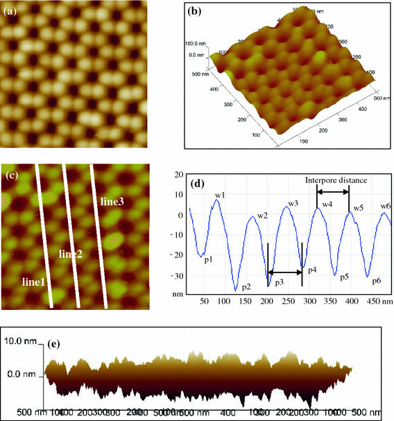
AFM images of PAA fabricated in 0.3 M oxalic acid at 0°C for 24 h with very good regulation (a) and its three-dimensional structure (b), c general AFM image of typical PAA fabricated in 0.3 M oxalic acid at 15°C for 1 h, d line profile analysis along line 2 indicated in c, and e height fluctuation profile of PAA surface by combining the X and Y axes. All images have an area of 500 nm × 500 nm
AFM has high resolution, and does not require the conductivity of samples, so it can be used to characterize PAAs with ultrasmall nanopore arrays, especially the pore diameter less than 20 nm. Figure 2a shows the ultrasmall PAA with the pore diameter of only 4–7 nm and sheet density as high as 2.0 × 1011 cm−2. To the best of our knowledge, it is the first time that PAA with less than 10 nm pore diameters and highest pore density is realized and characterized directly by AFM. It is interesting that the hexagonal cell structure cannot be detected, and that the pore diameter is not mainly controlled by the voltage any more for the ultrasmall PAAs. We will present more and have detailed discussion in another report for ultrasmall PAAs. In addition, AFM can be used to study the nucleation and growth mechanism by characterizing the surface morphology after anodization of different durations, such as 2, 3 and 10 s [7]. If a fluid cell is installed for some AFM equipments, it is possible to make real time observations of electrochemical reactions. As a result, it is possible to in situ obverse the nanopore growth process of PAA.
Figure 2.
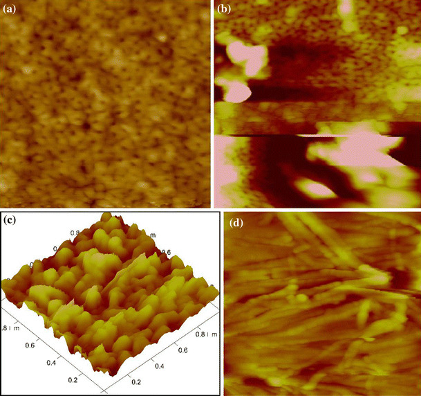
AFM images (500 nm × 500 nm) of a PAA fabricated in the mixture of 20 wt% H2SO4, 1 wt% citric acid and 1 wt% Al2(SO4)3 under 15°C and 10 V for 30 min, b PAA fabricated in 0.3 M oxalic acid under 15°C and 2 V for 30 min, c three-dimensional AFM image (1 μm × 1 μm) of PAA fabricated in 0.3 M oxalic acid under 15°C and 10 V for 30 min, d AFM image (1 μm × 1 μm) of PAA fabricated in a mixture of 0.3 M oxalic acid, 0.1 M Al2SO4 and 1 wt% ethylene glycol at 60°C for 30 min
But it is very hard to obtain perfect AFM images when the pore diameter is less than 20 nm because the fluctuation of surface height will severely affect the ultimate image even if the height of outstanding parts are only about several nanometers. Typical images are shown in Fig. 2b, 2c, it can be seen that they do have ultrasmall nanopores, but the surface “dirty” particle-like parts bring distortion of the real topology of the nanopores. Except the high requirement on the surface evenness, AFM technique can only characterize the surface morphology. Figure 2d shows the alumina nanowires obtained by anodizing aluminum under high temperature; however, the real configuration of this sample’s microstructure is very complicated (Fig. 3d).
Figure 3.
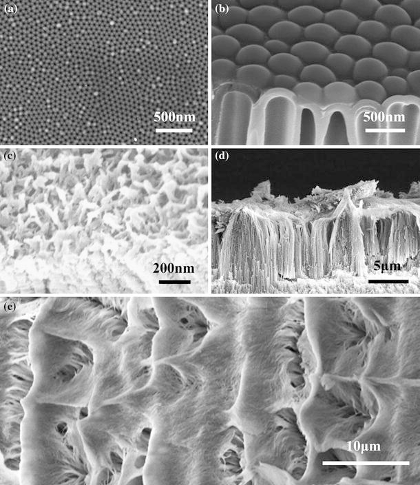
FESEM images of a the surface of typical PAA fabricated in 0.3 M oxalic acid under 5°C and 40 V for 10 h, b the cross-section of typical PAA fabricated in 5 wt% phosphoric acid under −1.5°C and 160 V for 6 h and pore widened in 5 wt% H3PO4 at 30°C for 1 h, c oblique view of PAA fabricated 0.3 M oxalic acid under 25°C and 40 V for 3 min and post-treated in 60°C deionized water for 1 h, d the cross-section of PAA fabricated in a mixture of 0.3 M oxalic acid, 0.1 M Al2SO4 and 1 wt% ethylene glycol at 60°C for 1 h, e the surface image of Fig. 3(d)
SEM Characterization
FESEM is the most commonly used method for observing PAAs’ microstructure, since FESEM can not only observe the surface, but also the transverse, tilt and cross-sections, as well as analyze the elemental composition by the energy dispersive X-ray analysis. Figure 3a, 3b is the typical surface and cross-sectional FESEM images of typical PAAs, respectively. The view field of FESEM is so wide that we can relocate the targets quickly, and that a systematically study on PAA microstructure can be accomplished in short time. Another advantage of FESEM is its low requirements on sample preparation, since the micro-scale roughness and nano-scale height fluctuations can be easily overcome by adjusting the distance between sample and probe and focusing process.
Complicated structures of PAA evolvements (modified, post-treated or tuned PAAs) can also be well characterized by FESEM due to previously mentioned advantages, as shown in Fig. 3c–3e. Figure 3c reveals that a lot of nanoscale protruding objects on the surface and nanoparticles in the nanopores of the PAA, which is fabricated in oxalic acid and treated in hot water. Figure 3d, 3e is the cross-sectional and surface images of nanowires standing on PAA, respectively, which is obtained by anodizing aluminum under higher temperature of 50–70°C in 0.3 M oxalic acid. The PAA nanopores transfer into nanowires due to partial dissolution of the pore wall under higher temperature, and the nanowires are so long that they collapse into some several-micron protruding bunches on the surface. AFM can detect the nanowires in a small area, such as 1 μm2, as shown in Fig. 2b, but it is very hard to characterize the nanowires and micro-scale bunches at the same time.
The most prominent advantage of FESEM characterization on PAAs is to observe the fracture sections including transversal, tilt and cross-sections, which can reveal a great deal of microstructure information. For the preparation of fracture sections, as is known to all, PAA is generated from aluminum substrate by anodization, and it is fragile due to its main composition of alumina, while the aluminum substrate has good toughness. So we can bend sample to make fracture sections of the PAA layer. Scratching the PAA layer with a diamond knife also works, as well as cutting the samples with a pair of scissors and looking for fracture section along the edges. Bending and scratching will bring better results than cutting since cutting will causes the deformations along the edges. Figure 4a is the cross-sectional view of PAA layer with the thickness ~500 nm upon aluminum substrate after bending, and it is clear that the PAA layer (highly order nanopore array structure) separates from the aluminum foil (bottom layer with disordered surface pattern in nanoscale). Figure 4b shows the low-magnification view of the bent sample, and many cracks can be found. By this method, we even have characterized PAAs with just 50 nm in thickness [21] Fig. 4c is the fracture sections realized by cutting the sample with a pair of scissors. The shearing effect makes the deformation of both PAA and aluminum layers happen, and as a result the fracture part is in a mess, and sometimes it is even hard to differentiate between aluminum and PAA layer. Carefully scratch the PAA layer with a diamond knife, and then we can find the fracture sections along the surface scratches, as shown in Fig. 4d. In addition, this approach can make the cracks with various depths (PAA pieces with different thickness in Fig. 4d), so more information of the specimen can be discovered.
Figure 4.
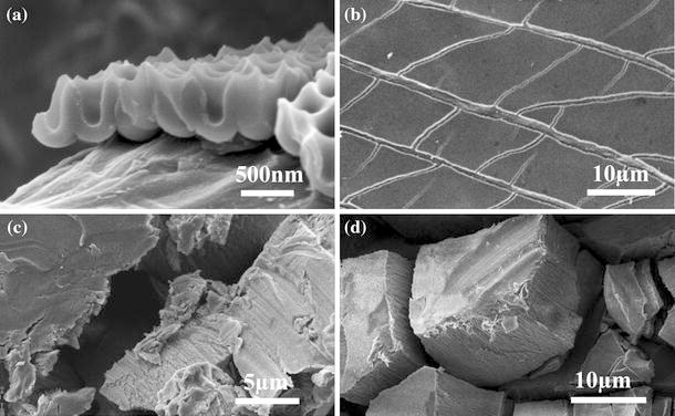
FESEM images of a the cross-section of PAA fabricated in 1 wt% H3PO4 under 0°C and 180 V for 10 min and bent before testing, b the low-magnification image of (a), (c) and (d) the fracture sections of PAA after cutting with a pair of scissors and scratching the surface with a diamond knife, respectively. The PAAs in c and d are fabricated in 5 wt% H3PO4 at 15°C for 30 min without second anodization
For the samples with thickness of more than 2 μm, it is possible to get the transverse and tilt sections, as well as cross-section, at the same specimen. Figure 5a is the typical example, showing three different kinds of regions (I, II and III) after scratching PAA layer. The region I (Fig. 5b) is the initial surface of sample. There are small pores in a big pore, which were archived by changing the applied potentials at the very beginning of anodizing process. The region II is an image of transverse section, which is parallel to the upper surface, as shown in Fig. 5c. The pore-in-pore surface morphology transforms into independent nanopores, and both shape and arrangement of these nanopores are not so ordered. The region III (Fig. 5d) is a tilt section indicating the fracture behavior of the individual nanopore.
Figure 5.
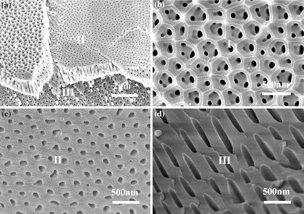
a FESEM image of scratched PAA showing three different regions (I, II and III), b region I of the original PAA surface, c region II of the transverse section, which is parallel to the surface, and d region III of the title section. The PAA is fabricated in a mixture of 0.5 wt% oxalic acid and 3 wt% citric acid under 140 V and 10°C for 20 min
We further reveal some special PAA evolvements to demonstrate the FESEM capability and to show the diversity and versatility of PAAs. Figure 6a shows a combined PAA configuration, which has upper PAA layer with larger nanopores and lower PAA layer with smaller nanopores, and the interesting transition process between the two layers can be understood based on FESEM images. Figure 6b shows another two-layer PAA structure with upper alumina nanotips and bottom nanopores. Figure 6c is three-layer configuration, which includes the special pore-in-pore upper layer, interlayer with small nanopore and bottom layer with large nanopores. No matter how many layers the PAA has, the thickness of each layer can be measured by the FESEM through carefully selecting the fracture sections and adjusting the sample stage, as shown in Fig. 6d. For good depth of field, FESEM can get clear image within a broad range of height difference, as shown in Fig. 6e (combined nanopore-microstep hierarchical structure) and Fig. 6f (upper aluminum micro-scale step structure with lower general PAA layer).
Figure 6.
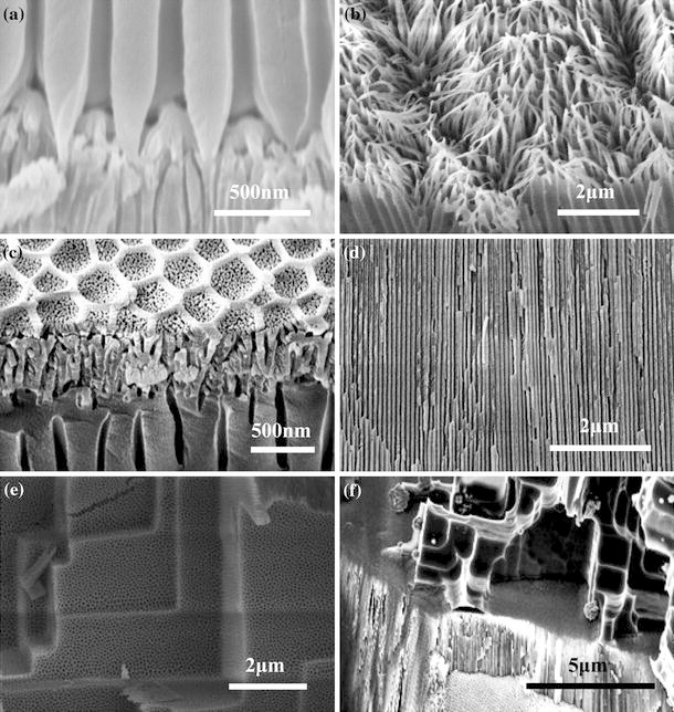
FESEM images of PAAs’ evolvements, a two-layer PAA sample with upper larger pores and bottom smaller pores, which is first anodized under 160 V at 0°C for 20 min in 5 wt% H3PO4 and second anodized 40 V at 30°C for 2 h in 0.3 M oxalic acid, b two-layer PAA structure fabricated under 180 V at 20°C in the mixture of 5 wt% phosphoric acid, 1 wt% citric acid and 5 wt% ethanol, c three-layer configuration by three-step anodization at 150 V for 1 min, 40 V for 25 min and 150 V for 1 h, d a typical cross-section of PAA fabricated under 40 V at 0°C in 0.3 M oxalic acid for 10 h, e combined nanopore-microstep hierarchical structure, which is obtained by first anodization under 5 V and 0°C in a mixture of 1 wt% H3PO4, 0.42 wt% NaCl and 20 wt% ethanol, and second anodization under 40 V and 40°C in 0.3 M oxalic acid, f upper aluminum micro-scale step structure with lower general PAA layer, which is obtained by first anodization in oxalic acid and second anodization on the other side in Cl− containing electrolyte until the current dropped dramatically. The anodizing condition in (f) is as same as that in (e)
All the Figs. 3, 4, 5 and 6 prove that FESEM technique is very useful and important for characterizing PAAs and their evolvements. But FESEM also has its shortage that the samples must have good electrical conductivity. It is well known that PAA is dielectric, so it needs to be coated with a very thin layer of platinum or aurum. Before FESEM measurement, the samples must be ultrasonically washed in acetone, and then thoroughly dried. Good electrical conductivity can be achieved by the smaller sputtering current and longer sputtering time with a direct current sputtering equipment. If the time is too long, or the current is too high, there are too much aurum grains deposited or the grains are too large. As a result, the real PAA microstructure may be covered by these grains. Sputtering iridium is best choice method with much higher cost because it can bring good conductivity, while the sputtered layer is just 1 nm in thickness. If PAA has a pore diameter around 10 nm, it is better to sputter iridium. If the conductivity is poor after sputtering, it will lead to quick color change during the scanning, or dull stripes in photos as shown in Fig. 7a, or unacceptable brightness variation. In addition, the poor conductivity may cause difficult focusing process and blurry photos, as showed in Fig. 7b, 7c. Generally, according to our experiences, thin PAAs (e.g. less than 1 μm) tend to have much better conductivity than thick PAAs (e. g. more than 10 μm) with the same Au sputtering process. So if only the pore diameter, pore shape and regularity are considered, fabricating thin PAAs is good choice for morphology characterization.
Figure 7.
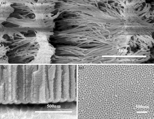
a FESEM images with dull stripes of PAA fabricated in 0.3 M oxalic acid under 40 V for 2 h and post-treated in 5 wt% H3PO4 at 30°C for 40 min, b and c blurry FESEM images of cross-section and top view of PAA fabricated in 0.3 M oxalic acid under 40 V and 0°C for 5 h
TEM Characterization
The studies on the characterization of PAA by TEM have been reported, especially during initial studies on anodic alumina many years ago since FESEM was not commonly used at that time [14,15,25]. Now with the improvements of TEM technique and PAA research, TEM can be used to observe not only the cross-sections, but also the surface. In order to characterize the surface, the PAA thickness should be carefully controlled within 100 nm since electrons need to go through the samples. Figure 8a is a typical TEM image showing the surface of PAA, which was obtained in 0.3 M oxalic acid under 40 V for a very short time. Compared to AFM and FESEM, TEM can observe and analyze a single hexagonal cell, and detect the element distribution, as well as test the crystal structure in the selected areas. For example, Thompson et al. [14] studied the nucleation and growth mechanism of PAA by TEM technique. We use TEM to study the ion distribution and its functionality for nanoscale assembly [26]. To observe the sections, the conventional method of sample preparation is to slice the sample and then reduce the thickness through ion beam thinning. But the thickness discrepancy in the sample will lead to color variation in obtained images (Fig. 8b). Considering the complicated process for sample preparation and not-so-good images, TEM is not convenient to characterize the PAA sections. TEM has no requirement on the conductivity of samples, thus it can be used to observe the PAA of smaller nanopores. For instance, Fig. 8c shows PAA TEM image with pore diameter of 15 nm.
Figure 8.
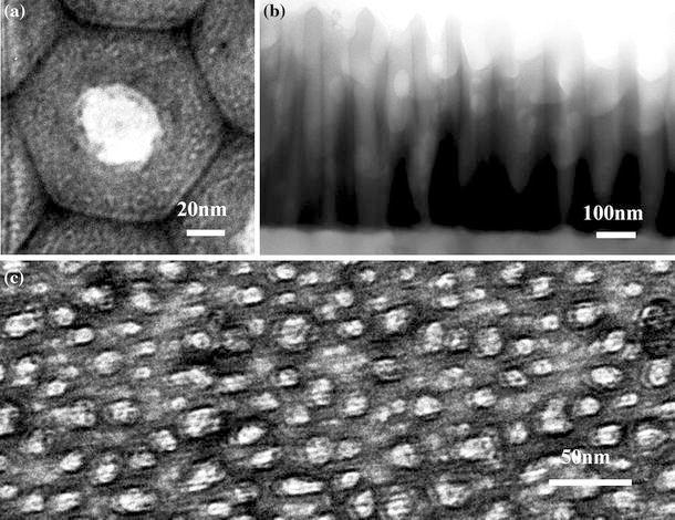
TEM images, a a single hexagonal cell of typical PAA fabricated in 0.3 M oxalic acid under 40 V at 0°C for just 1.5 min, b contrast variation in an image due to the thickness discrepancy in the sample that is fabricated in 0.3 M oxalic acid under 40 V at 0°C for 5 min c PAA with pore diameter of only 15 nm fabricated in 0.3 M oxalic acid under 12 V and 0°C for 3 min
Conclusions
We have AFM, FESEM and TEM studies on PAAs and their evolvements, and discuss the advantages and disadvantages of these methods. The main conclusions include the following:
1. The surface of general PAA samples can be easily characterized by AFM and FESEM. The element distribution and crystalline structure can be done with TEM.
2. The fracture characterization of PAA should be done with FESEM since it is most convenient and powerful to observe the transverse, tilt and cross-sections, the surface by bending the sample directly or scratching the surface with a diamond knife.
3. Ultrasmall PAAs with the pore diameter 5–20 nm should be characterized by AFM and TEM. AFM is better than TEM for this characterization.
4. PAA is very versatile since it has ordered hexagonal nanopore array and many evolvements that are obtained by post-treatments and tuning the fabricating process.
Acknowledgments
This work was supported by New Century Excellent Talents (NCET-04-0515), Qing Lan Project (2008-04), Key Programs for Science and Technology Development of Jiangsu (BE20080030), Changzhou Science and Technology Platform (CM2008301) and Key Laboratory of Material Tribology of Jiangsu (KJSMCX0902).
Open Access
This article is distributed under the terms of the Creative Commons Attribution Noncommercial License which permits any noncommercial use, distribution, and reproduction in any medium, provided the original author(s) and source are credited.
References
- Edwards JD, Keller F. Trans. 1941. p. 135. [DOI]
- Thompson GE, Wood GC. Nature. 1981. p. 230. COI number [1:CAS:528:DyaL3MXktFCqsrY%3D]; Bibcode number [1981Natur.290..230T] [DOI]
- Masuda H, Fukuda K. Science. 1995. p. 1466. COI number [1:CAS:528:DyaK2MXmtFKktbc%3D]; Bibcode number [1995Sci...268.1466M] [DOI] [PubMed]
- Chu SZ, Wada K, Inoue S, Isogai M, Yasumori A. Adv. 2005. p. 2115. COI number [1:CAS:528:DC%2BD2MXhtVaksbfJ] [DOI]
- Lee W, Ji R, Gösele U, Nielsch K. Nat. 2006. p. 741. COI number [1:CAS:528:DC%2BD28XovFyks74%3D]; Bibcode number [2006NatMa...5..741L] [DOI] [PubMed]
- Losic D, Lillo M, Losic D. Small. 2009. p. 1392. COI number [1:CAS:528:DC%2BD1MXotFKjsrg%3D] [DOI] [PubMed]
- Chen W, Wu JS, Xia XH. ACS Nano. 2008. p. 959. COI number [1:CAS:528:DC%2BD1cXksl2gurc%3D] [DOI] [PubMed]
- Sulka GD, Stepniowski WJ. Electrochim. Acta. 2009. p. 3683. COI number [1:CAS:528:DC%2BD1MXktlGmsLk%3D] [DOI]
- Bocchetta P, Ferraro R, Quarto FD. J. Power Sources. 2009. p. 49. COI number [1:CAS:528:DC%2BD1MXjsFykug%3D%3D] [DOI]
- Zhang DX, Zhang HJ. Microsc. 2006. p. 267. COI number [1:CAS:528:DC%2BD28XmslWjurc%3D] [DOI]
- Sui YC, Saniger JM. Mater. 2001. p. 127. COI number [1:CAS:528:DC%2BD3MXisVWhtb8%3D] [DOI]
- Rauf A, Mehmood M, Rasheed MA, Aslam M. Mater. 2009. p. 1601. COI number [1:CAS:528:DC%2BD1MXmsF2jsLY%3D] [DOI]
- Raimundo DS, Caliope PB, Huanca DR, Salcedo WJ. Microelectron. 2009. p. 844. COI number [1:CAS:528:DC%2BD1MXksVOhu70%3D] [DOI]
- Thompson GE, Furneaux RC, Wood GC, Richardson JA, Goode JS. Nature. 1978. p. 433. COI number [1:CAS:528:DyaE1cXltlKhuro%3D]; Bibcode number [1978Natur.272..433T] [DOI]
- Garcia-Vergara SJ, Skeldon P, Thompson GE, Habazaki H. Corros. 2008. p. 317.
- Smith JT, Hang QL, Franklin AD, Janes DB, Sands TD. Appl. 2008. p. 043108. Bibcode number [2008ApPhL..93d3108S] [DOI]
- Kwon N, Kim K, Heo J, Chung I. J. Vac. Sci. Technol. A. 2009. p. 803. COI number [1:CAS:528:DC%2BD1MXotFyisbk%3D] [DOI]
- Nagaura T, Takeuchi F, Inoue S. Electrochim. Acta. 2008. p. 2109. COI number [1:CAS:528:DC%2BD1cXhtV2jsw%3D%3D] [DOI]
- Tian YT, Meng GW, Gao T, Sun SH, Xie T, Peng XS, Ye CH, Zhang LD. Nanotechnology. 2004. p. 189. COI number [1:CAS:528:DC%2BD2cXjtVWrtbw%3D]; Bibcode number [2004Nanot..15..189T] [DOI]
- Sun QW, Ding GQ, Li YB, Zheng MJ, Shen WZ. Nanotechnology. 2007. p. 215304. Bibcode number [2007Nanot..18u5304S] [DOI]
- Ding GQ, Zheng MJ, Xu WL, Shen WZ. Nanotechnology. 2005. p. 1285. COI number [1:CAS:528:DC%2BD2MXhtVWgsb3J]; Bibcode number [2005Nanot..16.1285D] [DOI]
- Ding GQ, Shen WZ, Zheng MJ, Fan DH. Appl. 2006. p. 103106. Bibcode number [2006ApPhL..88j3106D] [DOI]
- Ding GQ, Shen WZ, Zheng MJ, Zhou ZB. Nanotechnology. 2006. p. 2590. COI number [1:CAS:528:DC%2BD28XntVWgsbk%3D]; Bibcode number [2006Nanot..17.2590D] [DOI] [PubMed]
- Ran CB, Ding GQ, Liu WC, Deng Y, Hou WT. Langmuir. 2008. p. 9952. COI number [1:CAS:528:DC%2BD1cXpvVars7s%3D] [DOI] [PubMed]
- Fratila-Apachitei LE, Tichelaar FD, Thompson GE, Terryn T, Skeldon P, Duszczyk J, Katgerman L. Electrochim. Acta. 2004. p. 3169. COI number [1:CAS:528:DC%2BD2cXjvFKksr0%3D] [DOI]
- Fan DH, Ding GQ, Shen WZ, Zheng MJ. Micropor. 2007. p. 154. COI number [1:CAS:528:DC%2BD2sXhsF2htr8%3D] [DOI]


