Abstract
We have studied the nucleation and growth of Se–Te nanowires (NWs), with different morphologies, grown by a chemical solution process. Through systematic characterization of the Se–Te NW morphology as a function of the Te nanocrystallines (NCs) precursor, the relative ratio between Se and Te, and the growth time, a number of significant insights into Se–Te NW growth by chemical solution processes have been developed. Specifically, we have found that: (i) the growth of Se–Te NWs can be initiated from either long or short triganol Te nanorods, (ii) the frequency of proximal interactions between nanorod tips and the competition between Se and Te at the end of short Te nanorods results in V-shaped structures of Se–Te NWs, the ratio between Se and Te having great effect on the morphology of Se–Te NWs, (iii) by using long Te nanorods as seeds, Se–Te NWs with straight morphology were obtained. Many of these findings on Se–Te NW growth can be further generalized and provide very useful information for the rational synthesis of group VI based semiconductor NW compounds.
Keywords: Selenium, Tellurium, Nanowires, Seeds
Introduction
One-dimensional (1D) nanostructures such as nanowires (NWs), nanobelts, nanorods, and nanotubes, have been the focus of intensive research due to their novel electronic properties and potential applications in nanoscale devices [1-6]. Among them, semiconductor NWs is investigated in more detail due to their important roles in fabricating nanoscale electronic or optoelectronic devices [7-11]. The growing interest in semiconductor NWs for electronic and photonic applications makes rational control over their morphology, structure, and key properties more and more important. It also requires thorough understanding of the growth mechanisms in specific material systems and techniques. Most group IV [12,13], III–V [14], and II–VI [15] semiconductor compounds NWs had been fabricated via the vapor–liquid–solid (VLS) mechanism successfully. By this method, a liquid metal alloy initiates the growth of a solid whisker from vapor reactants. Compared to the VLS method, solution phase reactions have the advantage that seeds are not restricted to a two-dimensional (2D) growth plane, and copious quantities of well-defined nanostructures can be obtained easily compared to methods based on vapor-phase reactions. Chemical solution NW growth for group VI semiconductor material systems was envisioned to occur via the solution–solid–solution mechanism, in which trigonal Se or Te seeds initiate the growth of solid Se, Te, or Se/Te alloy NWs from solution reactants. Traditionally, Se [16-18] and Te [19] NWs have been synthesized by reduced selenious acid or orthotelluric acid at elevated temperatures, typically at 90–100 °C or by the reduction of metal–salt solutions with ascorbic acid at room temperature, or by a mild bio-molecule-assisted reduction method under hydrothermal conditions. As Se and Te have similar trigonal structures, it is possible that Se/Te alloy NWs of a single crystalline nature can be obtained by reducing selenious acid and orthotelluric acid at the same time in solution. More importantly, as Te tends to form in the trigonal phase more readily than Se, one may fabricate Se/Te heterojunctions by using Te nanorods as crystalline seeds. Although Xia et al. [20] had synthesized Se–Te alloy nanorods successfully by reducing selenious acid and orthotelluric acid with hydrazine at the temperature range of 90–100 °C, the lateral dimensions and morphology of the Se/Te NWs could not be controlled in this case due to lack of any surfactant and exact experimental control. On the other hand, the use of a trigonal Te NCs as a crystalline seed in Se/Te NW growth has received less attention. Qian Research Group [21,22] had previously reported that by employing sodium dodecylbenzene sulfonate (SDBS) or other surfactants, Te nanorods with well controlled diameters and lengths could be reproducibly produced, which made the fabrication of Se/Te NWs by using Te NCs as crystalline seeds possible. Our research group [23] had further found that by using SDBS as the surfactant, the morphology and the lateral dimensions of Se/Te alloy NWs could be easily controlled. Following this, Se–Te alloy NWs with V-shaped structure has been prepared for the first time successfully by our research group with SDBS as surfactant [24].
In this article, we present new and simple methods for the fabrication of Se/Te NWs with different morphologies by using Te NCs seeds. We further investigated the nucleation and growth mechanism of Se–Te alloy with different morphology by controlling the experimental procedure. For the first time we have investigated the fabrication of Se/Te NWs with V-shape morphology, U-shape morphology, or straight morphology in the presence of SDBS surfactant by using different Te NCs seeds in detail. We prove here that such a method is a highly effective synthesis protocol to produce 1D nanostructures of Se/Te alloy NWs with different morphologies. Because of the mild reaction conditions and easily controlled synthesis, this method can be used in large-scale production of Te and Se/Te NW materials.
Experimental
Se/Te NWs were synthesized by a two-step solution process. First, fabrication of Te NCs by a chemical solution process similar to our previous report [23,24]. Typically, 2 mmol of orthotelluric acid and 0.5 g SDBS were added to 100 mL pure water. The solution was then refluxed for 1 h until a clear solution was obtained. Then, the resulting solution was heated up to 95 °C at a rate of 10 °C/min in an argon atmosphere. After 30 min, 1.5 mL of hydrazine was quickly injected into the solution through a syringe and the solution turned black and cloudy immediately. The solution was kept at 95 °C for another 15 mins and then moved to an ice bath to quench the reaction to 0 °C. The resulting solution was refluxed at room temperature for different time periods in order to get NWs with different lengths. To obtain short Te nanorods and nanoparticles, the reflux time is about 1 or 2 days while it takes at least 6 days to obtain long Te nanorods. Second, to obtain the V-shaped or U-shaped Se/Te NWs, the resulting solution, which was refluxed for about 1 day, was heated to 95 °C, and then a 15 mL solution containing 1 mmol, 2 mmol, or 4 mmol selenious acid was added drop by drop through a funnel into the resulting solution containing trigonal Te nanorods and colloids. The corresponding feeding ratio between Se to Te is 1:2, 1:1, and 2:1, respectively. The solution was refluxed at 95 °C for another 3 h and cooled down to room temperature. On the other hand, to obtain Se/Te NW with a straight morphology, the resulting solution that had been refluxed for 4 days was heated to 95 °C, and then a 15 mL solution containing 2 mmol selenious acid was added drop by drop through a funnel into the resulting solution which contains trigonal Te nanorods and colloids. The solution was refluxed at 95 °C for another 3 h and cooled down to room temperature.
Results and Discussion
The growth of Se/Te NWs was performed by using Te nanorods as crystalline seeds through a chemical solution process. The detailed process and growth parameters for the NWs growth can be found in the experiment procedure. Specifically, we have found that Te tends to form rod-shaped structures more easily than Se and hence has the highest surface reactivity along its spiral chain direction. Therefore, the Se/Te NWs are expected to form a wire-like structure by using the Te nanorod as the crystalline seed. In order to study the effect of feeding ratio (molar ratio) between Se and Te sources on the final morphology of Se/Te NWs, we investigated the TEM images of the Se/Te final product prepared by using short Te nanorods prepared at the same condition as crystalline seeds with different Se to Te feeding ratios.
Figure 1a (1b, 1c) shows the TEM image of Se/Te NWs fabricated under different conditions (with Se to Te feeding ratios 1:2, 1:1, and 2:1). Figure 1a1 (b1, c1) shows the corresponding diameter distribution of Se/Te NWs, while Fig. 1a2 (b2, c2) shows the angle deviation from the growth direction (showed in the inset of Fig. 1a). We found that the morphology is different for different Se to Te feeding ratios used during the reaction. First, we observed that the morphology is different from that of the Se/Te NWs with a straight morphology reported previously [23]. V-shaped and U-shaped Se/Te NWs were obtained in our case. Second, Se/Te NWs with a low Se feeding ratio (below 1:1) show an almost homogeneous distribution of V-shaped structures. No particles were found in the final product, which implies that all the amorphous Se or Te had been turned to triganol phase crystal structures during the reaction. In the case of V-shaped NWs, we found that the average NW length and NW diameter were about 150 nm and 13 nm, respectively, for all Se to Te feeding ratios. Third, for high Se feeding ratios, Se/Te NWs with all kinds of morphologies including V-shaped, U-shaped, and straight were obtained. From the distribution diagram of Se/Te NWs, we found that the angle deviation from the growth direction is from 25 to 40° depending on the different Se to Te feeding ratio (1:2 or 1:1). The angle distribution is in the range from 10 to 90° at high Se to Te feeding ratio (2:1). This implies that with a high Se feeding ratio, the strong competition between tellurium and selenium causes the growth direction to deviate from the regular direction.
Figure 1.
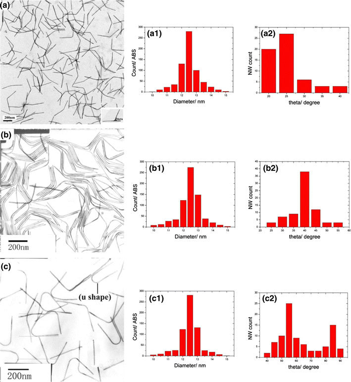
TEM images of t-Se/Te nanowires with different Se to Te molar ratio:aSe:Te = 1:2,bSe:Te = 1:1, andcSe:Te = 2:1 and their corresponding diameter (a1), (a2), (b1), deviate angle distribution schematic (b2), (c1), (c2)
As a comparison, we also synthesized Se/Te NWs by a similar chemical solution process using long Te nanorods as crystalline seeds; that is, the Te nanorods are prepared by refluxing the resulting solution containing Te nanocrystalline for 6 days at room temperature. The feeding ratio of Se to Te is 1:1 in this reaction. Shown in Fig. 2a is the Te nanorod crystalline seeds with a diameter of about 9.5 nm and length of about 150 nm. Figure 2b shows the TEM image of Se/Te NWs prepared by using such Te nanorod as the crystalline seeds. All the Se/Te NWs exclusively show a straight morphology which is quite different from the V-shaped or U-shaped Se/Te NWs prepared by using short Te nanorods as crystalline seeds. The diameter of each Se/Te NW is about 13 nm, larger than that of the Te crystalline seeds, while the length is about 300 nm, just two times that of the Te nanorods.
Figure 2.
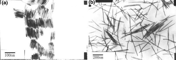
aTEM images of Te nanorods crystalline seeds prepared by a chemical solution process;bSe/Te NWs with straight morphology grown by using long Te nanorods with crystalline seeds
Figure 3 is the XRD patterns of the products obtained from the as-synthesized sample of Se–Te alloy NWs with different Se to Te ratio and pure Te crystalline seeds prepared by hydrazine reduction with SDBS as surfactant. The main diffraction peaks can be assigned to (100), (101), (110/102), (111), (200), (103), (210), (211), (212), (301) and (201/003) of Se/Te and (100), (101), (102), (111), (200), (201), (003), (202), (210), (212) and (301) of neat Te NWs. We find that the composition of Se/Te alloy NWs have little effect on the structure of as prepared samples. Other Se/Te alloy NWs prepared with different conditions has the same structure as those in Fig. 3. No peak of other impurities, such as amorphous Se or Te, is detected, implying the synthesis of high purity Te/Se and Te products and indicating that these alloy wires had been crystallized in a trigonal lattice similar to that of crystalline Se or Te, as reported in our previous studies [23].
Figure 3.
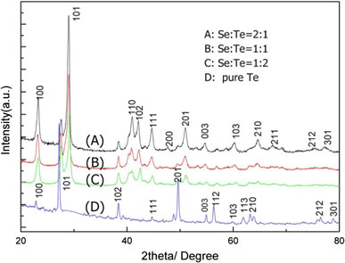
XRD pattern of the Se/Te NWs with different Se to Te ratio and pure Te NWs supported on a glass slide. All peaks can be indexed to the triangular Se/Te and Te lattice
We further performed a set of measurements including HRTEM and EDX to investigate the structure and Se, Te composition in different part of one single Se/Te NW. First, we characterized the composition of V-shaped and straight Se/Te NWs in different parts by Energy Dispersive X-Ray Spectroscopy (EDX) measurements (Fig. 4a, b). The atomic and weight percentage composition of Se and Te in different parts of a single NW is listed in Table 1. We noted that the composition of Se and Te in different parts of one single NW was quite different. In the middle part of V-shaped Se/Te NWs, the content of Te and Se was 57.1 and 42.9%, respectively. The content of Te decreased almost linearly from 57.1 to 36.9% (35.8% on another side) from the middle part to the end side, while Se increased from 42.9 to 63.1% (64.2% on anther side). We checked several single NWs and obtained similar results. In the case of straight Se/Te NWs, similar Se or Te content changes were found in different parts of single Se–Te NW. The Te content in the middle of the NWs is about 85.7%, the value of which is much higher than that of Se content (14.3%). The Te content decreases rapidly from the middle part to the end part. In the end part of a straight Se/Te NW, the value of Te content is 32.2 and 35.5%, respectively. On the other hand, Se content increased from 14.3 to 63.1% (67.8% in another side) from the middle part to the end part of Se/Te NW. All these observations clearly imply that the growth of the Se/Te NWs may be initiated from the middle part of the Se/Te NWs.Shown in Fig. 4c and d are the HRTEM images and Fast Fourier transforms image patterns (FFT, inset of Fig. 4) of V-shaped and straight NWs taken from the middle part of NW (①).
Figure 4.
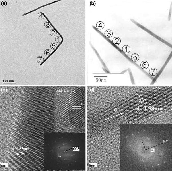
TEM images of 1D single Se/Te nanostructures prepared with SDBS as surfactant.aV-shape Se/Te;bstraight Se/Te NW and their corresponding HRTEM image(inset show the SEAD pattern); andc,dEDX taken from different part of one single V-shaped and straight Se/Te NW (①②③④⑤⑥⑦), the results have been listed in Table 1
Table 1.
EDS analysis of Se and Te content at different part of V-shape and straight Se/Te NW
| NW | Measure point | Se wt% | Te wt% | Se at.% | Te at.% |
|---|---|---|---|---|---|
| V-shape Se/Te NW |
4 |
51.4 |
48.6 |
63.1 |
36.9 |
| 2 |
45.6 |
54.4 |
57.4 |
42.6 |
|
| 3 |
37.4 |
62.6 |
49.1 |
50.9 |
|
| 1 |
31.8 |
68.2 |
42.9 |
57.1 |
|
| 5 |
37.7 |
62.3 |
49.4 |
50.6 |
|
| 6 |
44.9 |
55.1 |
56.8 |
43.2 |
|
| 7 |
52.6 |
47.4 |
64.2 |
35.8 |
|
| Straight Se/Te NW | 4 |
51.4 |
48.6 |
63.1 |
35.6 |
| 2 |
45.5 |
54.5 |
57.4 |
42.6 |
|
| 3 |
28.3 |
71.7 |
38.9 |
61.1 |
|
| 1 |
9.4 |
90.6 |
14.3 |
85.7 |
|
| 5 |
22.3 |
67.7 |
31.7 |
68.3 |
|
| 6 |
42.5 |
57.5 |
54.4 |
45.6 |
|
| 7 | 56.6 | 43.4 | 67.8 | 32.2 |
The FFT pattern was recorded by focusing a convergent beam on the NW. Since this pattern remained unchanged along the length of the NW, we concluded that this NW was essentially single crystalline in nature. HRTEM images show well resolved lattice fringes (in the (001) planes) of the Se/Te lattice, with the interplane spacing of 5.8 Å and 5.4 Å, respectively, which are between the values of trigonal Se (c = 4.953 Å) and Te (c = 5.921 Å), indicating that the NWs grow along the (100) direction. We also checked other parts of V-shaped (inset of Fig. 4c), and got similar results. The pattern indicates that these Se/Te NWs are single crystalline in nature and have predominantly grown along the [001] direction, with the helical chains of Se/Te atoms parallel to the longitudinal axis.
To further investigate the nucleation and evolution of V-shaped Se/Te NWs during growth, we monitored the morphological changes of the Se/Te NWs by TEM imaging for different growth times but otherwise identical growth conditions (with a Se to Te feeding ratio of 1:1). Before the Se sources addition, the product contained Te nanorods and some nanoparticles (Fig. 5a). The diameter of a typical Te nanorod is about 8 nm while the length is about 50 nm. After Se source addition, in a short growth interval (1 min), the apparent NW diameter increased to ~12.3 nm while the length increased to about 170 nm due to amorphous Se and Te nanoparticle resolved and deposited on the end and side wall of the Te nanorods. Some bending NWs were also observed at this point (Fig. 5b). The length and diameter of the NWs was observed to grow rapidly with increasing growth time. More and more V-shaped NWs were obtained after two minutes (Fig. 5c, d) following Se source addition. Figure 5e and f show histograms of average NW length and average diameter for different growth times. It is evident that the NWs start to grow with small diameters of about 8 nm. The diameter of each NW increases rapidly from 8 nm to 12 nm with 2 min of additional growth time after Se source addition, and then it grows slowly in diameter when we further increase the growth time. The diameter of the final product is about 13.5 nm, a little larger than that formed with a 2 min reaction. The length of the NWs increase rapidly from 50 nm to 170 nm, 288 nm, and 416 nm for growth times of 0, 1, 3, and 5 min after Se source addition. The increase in NW diameter and length indicates the formation of V-shaped Se/Te NWs based on how short Te nanorods finishes quickly upon Se source addition. Afterwards, there is almost no change even with an increase in the growth time. We obtain similar results when we use longer Te nanorods as the crystalline seed. The only difference is that only straight morphologies were obtained in the final Se/Te NW product. These results further suggest a growth mechanism different from the Se or Te that was generated in the same reaction solution through homogeneous nucleation, which takes a long time to finish, and provides further evidence that Te nanorods as crystalline seeds are necessarily initiating Se/Te NW growth, and that NW growth is nucleated by Te nanorods in our study.
Figure 5.
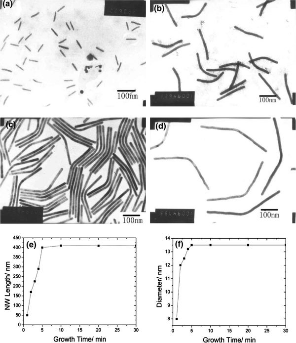
TEM images (a–d) of V-shape Se/Te NWs at different growth time after the addition of selenious acid into a solution containing short Te nanorods and nanoparticles and the statistical schematic of diameter and length of Se/Te NWs with growth time diffraction patterns (e,f) that support the mechanism outlined in Fig. 6.aMonodispersed short Te nanorods crystalline seeds and Te nanoparticles,b1 min,c3 min, andd5 min after the addition of selenious acid.eThe length of Se/Te NWs with growth time, andfthe diameter of Se/Te NWs with growth time
These experiments demonstrate that Te nanorods and SDBS surfactant play important roles in fabricating V-shaped and straight Se/Te NWs. Specifically, the observations that the content of Te in the middle part is higher than in the end part implies that Se/Te NWs grow from the middle part of the short or long Te nanorods. Shanbhag et al. [25] prepared for the first time V-shaped Te nanorods with a similar chemical solution process. They assumed that the incidence of nanoscale checkmark formation was governed by the frequency of proximal interactions between nanorod tips and based on the simulation results, they were able to explain why V-particles were observed for short nanorods while absent for long nanorods. We found that this mechanism can be used to explain the growth of Se/Te alloy NWs with different morphology in our case. However, we must point out that there are still some differences among them such as the preparation method. The Se and Te source are used in our case while only the Te source is used in their case and the using Te nanorods as crystalline seeds. The fact that there are no Se or Te nanoparticles in the final product indicates that the presence of Te nanorods is important for the single crystalline growth of Se/Te NWs. Study of the growth of Se/Te NWs has shown that the formation of V-shaped and straight Se/Te NWs in solution with SDBS as the surfactant involves several distinct stages: (1) the generation of short or long t-Te nanorods by adding N2H4 to reduce Te6+ in the solution with different refluxing times, (2) the formation of Se NCs when Se source was added drop by drop in the reacting solution, and (3) the a-Se and a-Te nanoparticles and some small Te nanorods dissolve into the solution during refluxing. The selenium and tellurium dissolved from a-Se, a-Te colloids and small t-Te nanorods could subsequently compete against each together and deposited on the surfaces of t-Te nanocrystallites (seeds). (4) trigonal Te nanorods(seeds) absorbed selenium and tellurium and grew into uniform, V-shaped or straight single crystalline NWs. The solid–solution–solid transformation, the anisotropic nature of the building blocks along the [001] direction of nanocrystalline Se/Te, and the surfactant-assisted preferentially unidirectional growth mechanism could be key factors in the formation of Se/Te NWs. Shown in Fig. 6 is a schematic image of a V-shaped Se/Te NW. Upon addition of hydrazine to the solution containing orthotelluric acid, the clear mixture immediately became black and opaque, indicating the formation of spherical colloids of Te NCs (Fig. 6a). Te NCs were produced through in situ reduction of orthotelluric acid with excess hydrazine: 2H6TeO6 + 3N2H4 → 2Te(↓) + 3N2(↑) + 12H2O. The formation of Te nanorods is similar to the Se/Te NWs reported in our previously published work [23]. When the selenious acid was added to the solution containing Te NCs and excess hydrazine, Se nanoparticles were produced immediately with hydrazine: H2SeO3 + N2H4 → Se(↓) + N2(↑) + 3H2O. The concentration of a-Se increases rapidly and will slowly dissolve into the solution during refluxing at relative high temperature (~90 °C) due to their higher free energies as compared to those of t-Se. The selenium and tellurium dissolved from a-Se, a-Te colloids, and some small t-Te nanorods can be subsequently deposited on the surfaces and the side wall of t-Te nanorods (seeds) (Fig. 6c). We must point out here that with the presence of SDBS surfactant, the growth of different planes of t-Te nanorods seeds is largely confined. We speculate that the sidewalls are mostly passivated by SDBS while the axial growth planes ([001] direction) are only partially passivated by SDBS. This has been confirmed by our experiment that the length of Te nanorods changes greatly while only a small change was observed in the diameter (Fig. 5). As a result, the growth rate of the (001) plane is much faster than that of other planes of t-Te nanorods (seeds). At high activity of short t-Te nanorods, the interactions between Te nanorod tips and the lattice constant mismatch in Se and Te. The competition between Se and Te at the end of short Te nanorods will result in the morphology change at the end of Te nanorods. The new Se/Te single crystalline surface formed at the end or the side wall of Te nanorods will act as new crystalline seeds and absorb the Se and Te dissolved from a-Se, a-Te colloids, and small t-Te nanorods in the solution. Finally, uniform V-shape or U-shape Se/Te NWs in the final products will be obtained after refluxing for several minutes. In the case of long Te nanorods, the frequency of proximal interactions between nanorod tips is low and we speculate that the concentration of tellurium is very low compared with selenium in the solution. The competition from Se and Te at the end of Te nanorods (seeds) is very weak. No morphology changes occur in this case and only Se/Te NW with straight morphology will be obtained in the final products.
Figure 6.
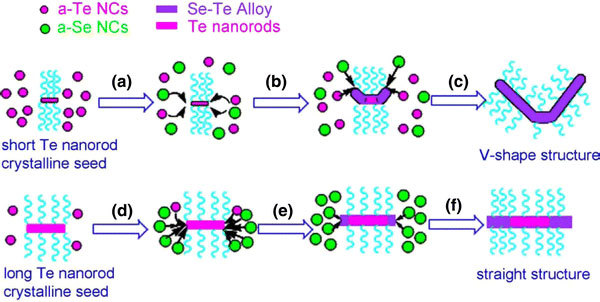
Schematic illustration of a plausible mechanism for the formation of V-shape Se/Te NW and straight Se/Te NW with SDBS as surfactant,aformation of a-Se nanoparticles when adding selenious acid into the solution containing short Te nanorods and nanoparticles,ba-Se and a-Te compete together and deposited at the end of Te nanorods crystalline seeds,cV-shape structure formation and continue to grow from the seeds accompanied by the dissolution of a-Se and a-Te colloidal particles as relax energy of Te nanorods at the end sides,dformation of a-Se nanoparticles when adding selenious acid into the solution containing long Te nanorods and few Te nanoparticles,ea small amount of a-Se and large quantity of a-Te compete together and deposited at the end of Te nanorods crystalline seeds, andfSe/Te NWs with straight morphology formation and continue to grow from the seeds accompanied by the dissolution of a-Te colloidal particles
Conclusions
In conclusion, we have studied the nucleation and growth evolution of Se/Te NWs prepared by chemical solution process. By varying key growth parameters such as using short Te nanorods or long Te nanorods as crystalline seeds, sequentially changing the Se to Te content, growth time, first time significant insights into the Se/Te NWs with different morphology growth have been developed. The trigonal Te nanorods were found to have the major role on the growth of single crystalline Se/Te NWs, while the present of SDBS surfactant is necessary to restrain the grow direction of Se/Te NWs. V-shape or U-shape Se/Te NWs are most likely formed by the competition of selenium and tellurium at the end of Te nanorods (seeds) and by the frequency of proximal interactions between nanorod tips. This conclusion is also supported by the analysis of Se and Te content in different part of Se/Te NW by EDAX. The input SDBS surfactant was shown to play a critical role in NW growth. These findings are very useful for understanding and rational synthesis of Se/Te NWs or other VI group compound semiconductor NWs.
Acknowledgment
This work is supported by NSFC project (No 50703012) and the MOST project (Nos 2009CB930604 and 2009CB623602).
References
- Lieber CM, Wang ZL. MRS Bull. 2007. p. 99. COI number [1:CAS:528:DC%2BD2sXjsVOlsrk%3D]
- Li Y, Qian F, Xiang J, Lieber CM. Mater. Today. 2006. p. 18. COI number [1:CAS:528:DC%2BD28XhtFCht7nO] [DOI]
- Duan X, Huang Y, Cui Y, Wang J, Lieber CM. Nature. 2001. p. 66. COI number [1:CAS:528:DC%2BD3MXkt1WqsA%3D%3D]; Bibcode number [2001Natur.409...66D] [DOI] [PubMed]
- Huang HM, Mao S, Feick H, Yan H, Wu Y, Kind H, Weber E, Russo R, Yang P. Science. 2001. p. 1897. COI number [1:CAS:528:DC%2BD3MXksVaqsb0%3D]; Bibcode number [2001Sci...292.1897H] [DOI] [PubMed]
- Schoen DT, Xie C, Cui Y. J. 2007. p. 4116. COI number [1:CAS:528:DC%2BD2sXivF2jsbk%3D] [DOI] [PubMed]
- Takeda S, Nakamura M, Ishii A, Subagyo A, Hosoi H, Sueoka K, Mukasa K. Nanoscale Res. 2007. p. 207. COI number [1:CAS:528:DC%2BD2sXmvFyltrc%3D]; Bibcode number [2007NRL.....2..207T] [DOI] [PMC free article] [PubMed]
- Dayeh SA, Yu ET, Wang D. Small. 2007. p. 1683. COI number [1:CAS:528:DC%2BD2sXhtFyit7bP] [DOI] [PubMed]
- Hullavarad SS, Hullavarad NV, Karulkar PC, Luykx A, Valdivia P. Nanoscale Res. 2007. p. 161. COI number [1:CAS:528:DC%2BD2sXktVartLs%3D]; Bibcode number [2007NRL.....2..161H] [DOI]
- Novotny CJ, Yu ET, Yu PKL. Nano Lett. 2008. p. 775. COI number [1:CAS:528:DC%2BD1cXhvVGgtL4%3D]; Bibcode number [2008NanoL...8..775N] [DOI] [PubMed]
- Dayeh SA, Aplin DPR, Zhou X, Yu PKL, Yu ET, Wang D. Small. 2007. p. 326. COI number [1:CAS:528:DC%2BD2sXhvFWht7s%3D] [DOI] [PubMed]
- Qin D, Tao H, Zhao Y, Lan L, Chan K, Cao Y. Nanotechnology. 2008. p. 355201. [DOI] [PubMed]
- Wang D, Wang Q, Javey A, Tu R, Dai H, Kim H, McIntyre PC, Krishnamohan T, Saraswat KC. Appl. 2003. p. 2432. COI number [1:CAS:528:DC%2BD3sXnsVWhsLY%3D]; Bibcode number [2003ApPhL..83.2432W] [DOI]
- Cui Y, Zhong Z, Wang D, Wang W, Lieber CM. Nano Lett. 2003. p. 149. COI number [1:CAS:528:DC%2BD3sXhtl0%3D]; Bibcode number [2003NanoL...3..149C] [DOI]
- Huang Y, Duan XF, Cui Y, Lieber CM. Nano Lett. 2002. p. 101. COI number [1:CAS:528:DC%2BD38Xislamtw%3D%3D]; Bibcode number [2002NanoL...2..101H] [DOI]
- Goldberger J, Sirbuly D, Law M, Yang P. J. Phys. Chem. B. 2005. p. 9. COI number [1:CAS:528:DC%2BD2cXhtVKitL7J] [DOI] [PubMed]
- Ren L, Zhang H, Tan P, Chen Y, Zhang Z, Chang Y, Xu J, Yang F, Yu D. J. Phys. Chem. B. 2004. p. 4627. COI number [1:CAS:528:DC%2BD2cXitFektbg%3D] [DOI]
- Gates B, Yin Y, Xia Y. J. 2000. p. 12582. COI number [1:CAS:528:DC%2BD3cXotl2ntrg%3D] [DOI]
- Li Q, Yam VWW. Chem. Commun. (Camb.) 2006. p. 1006. [DOI] [PubMed]
- Mayers B, Xia Y. J. 2002. p. 1875. COI number [1:CAS:528:DC%2BD38XjvFWjsLc%3D] [DOI]
- Mayers B, Gates B, Yin Y, Xia Y. Adv. 2001. p. 1380. COI number [1:CAS:528:DC%2BD3MXntFWitLk%3D] [DOI]
- Liu Z, Hu Z, Xie Q, Yang B, Wu J, Qian Y. J. 2003. p. 159. COI number [1:CAS:528:DC%2BD38XpsValsr0%3D] [DOI]
- Liu Z, Hu Z, Liang J, Li S, Yang Y, Peng S, Qian Y. Langmuir. 2004. p. 214. COI number [1:CAS:528:DC%2BD3sXovFOgtrk%3D] [DOI] [PubMed]
- Qin D, Zhou J, Luo C, Liu Y, Han L, Cao Y. Nanotechnology. 2006. p. 674. COI number [1:CAS:528:DC%2BD28Xis1yhs70%3D]; Bibcode number [2006Nanot..17..674Q] [DOI] [PubMed]
- Qin D, Tao H, Cao Y. Chin. 2007. p. 670. COI number [1:CAS:528:DC%2BD1cXhvVSru78%3D] [DOI]
- Shanbhag S, Tang Z, Kotov NA. ACS Nano. 2007. p. 126. COI number [1:CAS:528:DC%2BD2sXhtFSnsL%2FL] [DOI] [PubMed]


