Abstract
Large-scale bunch-like bismuth (Bi) nanostructures were the first time to be synthesized via two-step electrochemical deposition. The growth mechanism of the nanostructures was discussed. Such a designed bunch-like Bi electrode has high sensitivity to detect the heavy metal ions due to its unique three-dimensional structures and strong ability of adsorbing the heavy metal ions. The bunch-like Bi electrode’s detection of heavy metals was statically performed using anodic stripping voltammetry (ASV). The detection in the Pb(II) concentration range of 2.5–50 μg/l was also performed. Based on the experimental results, this bunch-like Bi electrode can be considered as an interesting alternative to common mercury electrodes and bismuth film electrodes for possible use in electrochemical studies and electroanalytical applications.
Keywords: Bismuth, Nanostructure, Electrochemical deposition
Introduction
Mercury electrode has gained wide acceptance for the electrochemical stripping analysis of heavy metal. However, the toxicity of mercury and its difficulties in handling, storage, and disposal may severely restrict its use as an electrode material [1-5]. Recently, a bismuth electrode as a favorable replacement for a mercury electrode has been introduced, because of behavior similar to the mercury electrode and the environmentally friendly nature of bismuth [6-10].
To date, the research of the bismuth electrode mainly focused on the bismuth film electrodes (BiFEs) [11-16]. However, the three-dimensional nanostructures with large specific surface area and high surface free energy, which is superior to the film in the chemical sensor applications, have aroused much attention in recent years. In addition, electrochemistry offers convenient and elegant techniques for the fabrication of nanostructures [17,18]. The properties of these nanostructures can be controlled by their electrochemical potential, a variable that is not available in vacuum or in air. Therefore, a three-dimensional ordered bismuth electrode formatted via the electrochemistry method should be an ideal electrode for effectively improving the properties of detecting heavy metal ions.
Herein, a new self-organized morphology of Bi (the bunch-like Bismuth) is the first time to be prepared by a two-step template synthesis using electrodeposition. The growth habits and growth mechanism of this electrode were discussed. On account of the unique structure, this morphology of bismuth has been at the first time studied as an electrode, which has a good performance to detecting the heavy metal ions.
Experiment
Reagents
The electrolyte solution contained 20 g/l BiCl3, 50 g/l tartaric acid, 95 g/l glycerol, and 70 g/l NaCl at room temperature. The pH of the solution was strictly controlled at a value of 2 by the addition of nitric acid. Stock solution of 0.01 M Pb2+, Cd2+, Hg2+, Cu2+ was prepared by dissolving Pb(NO3)2, Cd(NO3)2, Cu(NO3)2, HgCl2(Shanghai Reagent Corporation, China) in deionized water and then diluted to various concentrations of working solutions. 0.2 M HAc-NaAc buffer solutions (pH: 4.4) were used as the supporting electrolyte for heavy metal determination.
Apparatus
All electrochemical experiments were performed with a CHI660C (Chen Hua Shanghai, China) workstation at room temperature, employing a three electrode system consisting of a saturated calomel electrode (SCE) reference electrode, an alumina/Au composite working electrode (with diameter of 4.0 mm), and a Pt wire counter electrode. Mesh-like thin Au layer only covering the surface of the membrane and still leaving the pores open was sputtered on one planar surface side of the AAO template to make the surface electrically conductive, and a Cu wire was connected to the Au layer with Ag paint. The Au side and edges of the alumina template were then insulated with clear nail polish to ensure the electrodeposition could only occur on the other side of the AAO.
Preparation and Analytical Procedure
A potential of −1.5 V was applied between cathode and anode. The pulse time was 0.4 ms and the time between pulses was 0.8 ms. After deposition of 40 min, the nano bismuth electrode array was fabricated. Step 2: a potential of −2.5 V was applied, the bunch-like Bi microstructures were fabricated, respectively. SWASV was performed under the following conditions:Edep, −1.1 V for 60 s;Esw, 25 mV;Estep, 5 mV;f, 50 Hz; scan range, −1.2–0 V.
Results and Discussion
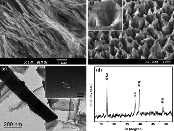
Typical scanning electron microscopy (SEM) and the transmission electron microscopy (TEM) images of the as-synthesized products are given in Fig. 1. Figure 1a shows the image of Bi nanowire arrays fabricated by pulsed electrodeposition. The Bi nanowires embedded in anodic alumina membrane (AAM), and gradually, the nanowires began to grow out of the AAM. High filling, ordered, and uniform Bi nanowires were produced in the AAM. Figure 1b shows the SEM image of bunch-like Bi electrode, which was synthesized via two-step electrochemical deposition. From the SEM images, we can find that they are mostly bunch-like. It indicates that large-scale bunch-like superstructures composed of many nanowires with a diameter of about 100 nm can be obtained under the present experimental conditions. Some Bi nanowires bent down and get together on the top, which causes a large space in the middle. Meanwhile, the nanowires have their ends assembled that fabricates like bunches. The space among bunches like a nest can be seen from the high-magnification SEM image (the inset in Fig. 1b), and the diameter of the nest is about 10 μm. Figure 1c is the representative TEM image of Bi nanowires with a diameter of 100 nm. The inset of Fig. 1c shows that the inter planer spacing is about 0.23 nm corresponding to the lattice fringes of (110) planes, which further confirms that the nano Bi electrodes are grown along the [110] direction, which is consistent with the XRD result. Figure 1d illustrates the XRD pattern of the as-grown products. Most of the peaks are indexed to the typical hexagonal rhombcentered phase bismuth (JCPDS No. 05-0519). The sharp and narrow XRD peaks indicate that the bunch-like Bi have good crystalline order, and the peak at 2θ = 27.1°, 38.0°, 39.7°, are very strong when compared with other peaks, indicating a highly preferential orientation of the nanowires, respectively, along the [012], [104], and [110] direction, indicating that the resultant products are highly crystallized elemental bismuth with a high purity under the current synthetic conditions.
Figure 1.

a SEM image of Bi nanowires embedded in AMM and grown out of the membranes. b SEM image of the bunch-like Bi composed of Bi nanowires. The inset shows the nest formed by the nanowires. c TEM image of individual Bi nanowires embedded in the AAM. The inset shows the corresponding lattice fringe image. d Typical XRD pattern of the prepared bunch-like Bi electrode
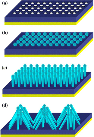
We supposed the growth mechanism of the bunch-like Bi as follows: at the beginning of deposition, Bi nanowires embedded in the AAM were fabricated by pulsed electrodeposition. After the nanowires grew out of the membranes, the Bi nanowire array formed the nano electrode array, which acted as the cathode in the following deposition. We conjectured the reason that leads to the nanowires changing into bunch was principally attributed to the electric field. When a vertical electric field was applied to Bi nano electrode array, the nanowires were all bent down, all the neighboring nanowires had their ends assembled and knitted together from different orientations, forming the bunches and the nests of the bunch-like bismuth microstructure. The growth of these Bi nanoparticles proceeds to nanowires, self-assembly, and finally to the bunch-like bismuth, which is depicted in the Fig. 2.
Figure 2.

Schematic for the synthesis of bunch-like bismuth that can be achieved via two-step electrodeposition. a Sputtering a mesh-like Au layer (the yellow layer) on one planar surface side of the AAM (the deep blue layer). b Electrodepositing bismuth (the light green rods) into the AAM, the bismuth begin to grow out of the membranes. c DC deposition continued, the nanowire became longer and thinner. d The neighboring nanowires had their ends assembled and knitted together from different orientations
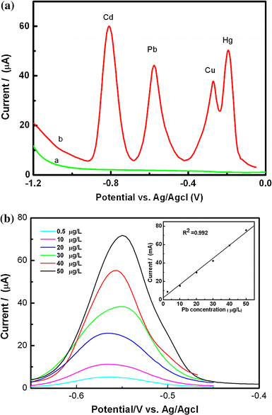
Figure 3a shows square wave anodic stripping voltammograms (SWASVs) of the heavy metal ions (Pb2+, Cd2+, Cu2+, Hg2+) at the bunch-like bismuth electrode. Compared with the voltammogram of the electrode in pure supporting electrolyte (green line), all the heavy metal ions show well-defined anodic peaks at the bunch-like bismuth electrode (red line). The peak potential of Cd2+, Pb2+, Cu2+, and Hg2+ at the bunch-like bismuth is −0.81, −0.58, −0.30, and −0.19, respectively. When comparing the anodic stripping voltammetry measurements of the same trace heavy metals obtained at the in situ prepared bismuth film electrodes (BiFEs) and the bunch-like bismuth under the same conditions, it is observed that anodic peak current of the heavy metals at the bunch-like bismuth electrode have a little negatively shift, respectively [19]. The negative shifts in the anodic peak potentials of the heavy metals indicate that the oxidation of the heavy metals at the bunch-like bismuth electrode is thermodynamically more favorable. The increases in anodic peak current are attributed to difference in the crystalline structure or in the morphology (roughness) of the BiFE and the bunch-like bismuth surfaces. This may affect the preconcentration efficiency at the bunch-like bismuth electrode, which is assumed to contribute to its relatively lower stripping voltammetry response. As an example, Pb(II) at different concentrations ranging from 2.5 to 50 μg/l was measured in the acetate buffer using the bunch-like Bi nanoelectrode, which was illustrated in the Fig. 3b. The corresponding calibration plot for Pb(II) was linear over the range of 2.5–50 μg/l (R2 = 0.992), as shown in Fig. 3b, which reveal the high correlation between the peak current recorded and the concentration of metal in the sample.
Figure 3.

Square-wave anodic stripping voltammograms recorded with the bunch-like bismuth electrode a blank 0.1 mol/l acetate buffer pH 4.4b 40 μg/l of Pb2+, Cd2+, Cu2+, Hg2+
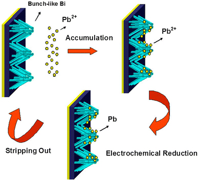
In principle, the analysis of heavy metal ions (take Pb2+ for example) using ASV method has three main steps, including accumulation, electrochemical reduction, and stripping out. The combination of accumulation and reduction prior to the stripping detection process can enhance both the sensitivity and the selectivity of the analysis of metal ions. The efficiency of the first two steps plays a great role in the entire analysis. The use of the bunch-like Bi electrode with a porous nanostructure can greatly promote the surface area and high surface-free energy, which is beneficial for the adsorption of the metal ions. Accumulation of Pb2+ on bunch-like Bi electrodes at open-circuit potential was performed by immersing the electrode into the stirred Pb(NO3)2 solution (300 rpm) for 8 min. In this step, lead ions can combine with the wall fabricated by enormous Bi nanowires on the electrode surface after accumulation. The Pb2+ deposited on the electrode under cathode potentiostatic conditions (−1.1 V) for a defined time period (60 s). Finally, the accumulated lead ions were stripped off the electrode and the stripping current was measured. The diagrammed illustration is presented in Fig. 4.
Figure 4.

Schematic diagram for stripping analysis of Pb2+, including accumulation, electrochemical reduction, and stripping out
Conclusions
In summary, we have successfully fabricated a single-crystalline bunch-like Bi nanostructure using a two-step electrodeposition in anodic alumina membranes for the first time. We have demonstrated that the stripping voltammetric performance of this bunch-like bismuth electrode compares favorably with that of common mercury-based electrodes. The higher sensitivity of the bunch-like bismuth electrodes makes it suitable for detecting metals more sensitive than other bismuth electrode.
Acknowledgments
The authors acknowledge the financial support from the Chinese National Key Basic Research Special Found (Grant No. 2006CB921704), the NSF of China (Grant No. 60976014), and the Key Basic Research Project of Scientific and Technology Committee of Shanghai (Grant No. 09DJ1400200).
Open Access
This article is distributed under the terms of the Creative Commons Attribution Noncommercial License which permits any noncommercial use, distribution, and reproduction in any medium, provided the original author(s) and source are credited.
References
- Wang J. Electroanalysis. 2005. p. 1341. COI number [1:CAS:528:DC%2BD2MXpsFCqt7Y%3D] [DOI]
- Economou A, Fielden PR. Talanta. 1998. p. 1137. COI number [1:CAS:528:DyaK1cXkslSitbY%3D] [DOI] [PubMed]
- Wang J. Stripping Analysis. Vch, Deerfiled Beach, FL; 1985. [Google Scholar]
- Jones S, Compton RG. Curr Anal Chem. 2008. p. 170. COI number [1:CAS:528:DC%2BD1cXnsVGmtbg%3D] [DOI]
- Daniele S, Baldo MA, Bragato C. Curr. 2008. p. 215. COI number [1:CAS:528:DC%2BD1cXnsVGmurw%3D] [DOI]
- Kokkinos C, Economou A. Curr. 2008. p. 183. COI number [1:CAS:528:DC%2BD1cXnsVGmtbY%3D] [DOI]
- Svancara I, Baldrianova L, Tesarova E, Hocevar SB, Elsuccary SAA, Economou A, Sotiropoulos S, Ogorevc B, Vytras K. Electroanalysis. 2006. p. 177. COI number [1:CAS:528:DC%2BD28XhtFGht74%3D] [DOI]
- Stozhko NY, Malakhova NA, Fyodorov MV, Brainina KZ. J. 2008. p. 1185. COI number [1:CAS:528:DC%2BD1cXnvVOms78%3D] [DOI]
- Stozhko NY, Malakhova NA, Fyodorov MV, Brainina KZ. J. 2008. p. 1219. COI number [1:CAS:528:DC%2BD1cXnvVOms70%3D] [DOI]
- Honeychurch KC, Hart JP. Trends Anal. 2003. p. 456. COI number [1:CAS:528:DC%2BD3sXls1Sqtrs%3D] [DOI]
- Zhu X, Gao C, Choi JW, Bishop PL, Ahn CH. Lab Chip. 2005. p. 212. COI number [1:CAS:528:DC%2BD2MXmsV2itQ%3D%3D] [DOI] [PubMed]
- Baldo MA, Daniele S. Anal. 2004. p. 995. COI number [1:CAS:528:DC%2BD2cXislyqsL0%3D] [DOI]
- Demetriades D, Economou A, Voulgaropoulos A. Anal. Chim. Acta. 2004. p. 167. COI number [1:CAS:528:DC%2BD2cXmt1Kgsbc%3D] [DOI]
- Baldrianova L, Svancara I, Vlcek M, Economou A, Sotiropoulos S. Electrochim. Acta. 2006. p. 481. COI number [1:CAS:528:DC%2BD28XhtVWrsLzL] [DOI]
- Economou A. Trends Anal. 2005. p. 334. COI number [1:CAS:528:DC%2BD2MXivVKru7Y%3D] [DOI]
- Kokkino C, Economou A, Raptis I, Efstathiou CE, Speliotis T. Electrochem. 2007. p. 2795. [DOI]
- Li CZ, Bogozi A, Huang W, Tao JJ. Nanotechnology. 1999. p. 221. Bibcode number [1999Nanot..10..221L] [DOI]
- He HX, Boussaad S, Xu BQ, Li CZ, Tao NJ. J. 2002. p. 167. COI number [1:CAS:528:DC%2BD38XivFOhsLc%3D] [DOI]
- Wang J, Lu J, Hocoeevar SB, Farias PAM, Ogorevc B. Anal. 2000. p. 3218. [DOI] [PubMed]


