Abstract
Dielectrophoresis has been used in the controlled deposition of single-walled carbon nanotubes (SWNTs) with the focus on the alignment of nanotube thin films and their applications in the last decade. In this paper, we extend the research from the selective deposition of SWNT thin films to the alignment of small nanotube bundles and individual nanotubes. Electrodes with “teeth”-like patterns are fabricated to study the influence of the electrode width on the deposition and alignment of SWNTs. The entire fabrication process is compatible with optical lithography-based techniques. Therefore, the fabrication cost is low, and the resulting devices are inexpensive. A series of SWNT solutions is prepared with concentrations ranging from 0.0125 to 0.2 mg/ml. The alignment of SWNT thin films, small bundles, and individual nanotubes is achieved under the optimized experimental conditions. The electrical properties of these samples are characterized; the linear current–voltage plots prove that the aligned SWNTs are mainly metallic nanotubes. The microscopy inspection of the samples demonstrates that the alignment of small nanotube bundles and individual nanotubes can only be achieved using narrow electrodes and low-concentration solutions. Our investigation shows that it is possible to deposit a controlled amount of SWNTs in desirable locations using dielectrophoresis.
Keywords: Single-walled carbon nanotubes (SWNT), Dielectrophoresis (DEP), Thin film, Nanotube bundle, Individual nanotube, Deposition
Introduction
Carbon nanotube (CNT) is a unique form of carbon material with remarkable physical, chemical, and electrical properties [1]. It has attracted considerable attention in the last 20 years. CNTs have a high potential in a great number of applications, especially in nanoelectronics and biomedical sensors. A wide variety of electronic devices based on individual single-walled carbon nanotubes (SWNTs) or SWNT thin films have been successfully developed and used as sensors [2-4], field-effect transistors [5,6], conductive interconnects [7,8], and energy storage systems [9,10]. A critical step to obtain these practical devices is to deposit well-organized and highly aligned SWNTs in desired locations. Recently, researchers have developed a number of methods to align SWNTs: using moving fluids to organize nanotubes [11], introducing gas flows in reactors or channels [12], withdrawing microfluidic channels from solutions [13], spin coating nanotube dispersions with controlled speeds [14,15], and magnetic capturing of nanotubes [16]. However, many of these techniques have limitations and restrictions, because they require either intensive preparation processes or assisting materials with special properties. Therefore, their applications are relatively limited.
In comparison, dielectrophoresis, a simple but versatile method, has proven to be effective in aligning SWNTs in small and large scales [17,18]. This method can be conducted at room temperature with low voltages. In addition, a number of parameters such as solution concentration, deposition time, AC source amplitude, and frequency can be adjusted to optimize the quality of the aligned SWNTs. More importantly, dielectrophoresis can be easily incorporated into device fabrication [19,20] and eventually used in wafer-level-controlled deposition [21]. Recently, devices based on dielectrophoresis-aligned SWNTs have been developed and used as biocompatible substrates for cell growth [22], bacteria capturing chips [23], gas sensors [24], and memory devices [25]. Numerical studies have also been performed to provide theoretical support of the process [26,27]. However, most of these research efforts are focused on the alignment of SWNT thin films. Even though the controlled assembly of single SWNT bundles has been studied by using various voltage magnitudes and types [28], a thorough investigation into electrode geometry and solution concentration is still necessary to achieve the precise alignment of individual SWNTs and small nanotube bundles.
In this paper, we examine the selective deposition of SWNTs with dielectrophoresis to obtain aligned nanotubes in the form of thin films, small bundles, and individual nanotubes. These different results are achieved by changing a number of parameters in the dielectrophoresis process and the SWNT samples. Pristine SWNTs are treated with acids for surface functionalization and diluted with deionized (DI) water to obtain different concentrations. The SWNT thin films are deposited and aligned using a large-width electrode design; the alignment of nanotube bundles and individual nanotubes is achieved by using a small-width “teeth”-like electrode design. The “teeth”-like electrodes are used to induce concentrated and highly directional electric field in between two opposite “teeth”. Consequently, the electric field attracts SWNTs to this location and rotates them to follow the electric field lines. The electrodes are fabricated with optical lithography and wet etching; expensive equipment, such as electron-beam writer, commonly used in the fabrication of individual nanotube devices is avoided. The dielectrophoresis experiments are conducted at room temperature. Scanning electron microscopy (SEM) inspection shows that the SWNTs are well aligned in desired locations. Electrical characterization of these SWNT devices demonstrates that they have linear current–voltage (I–V) curves, and their resistance is dependent on the SWNT solution concentration. The fabrication steps, the dielectrophoresis process, the quality of the aligned nanotubes and thin films, and the characterization results are described and discussed in this paper.
Dielectrophoresis
When dielectric particles are exposed to a non-uniform electric field, charges including electrons and protons are moved from their initial balanced positions and redistributed in these particles. The charge redistribution creates electric dipole moments and forces these particles to rotate along the electric field lines. The induced effective dipole moment for an ellipsoidal particle can be expressed as [29]:
where V is the volume of the particle, εp and εm are the permittivities of the particle and the medium, E is the external electric field strength, AL ≈ 4r2/l2[ln (l/r) − 1] is the depolarization factor, and r, l are the radius and length of the ellipsoidal particle, respectively.
Similarly, the external non-uniform electric field can induce dipole moments in rod-like objects including nanowires and carbon nanotubes. The dipole moment parallel to the tube axis is much stronger than that in the perpendicular direction. Therefore, the polarized nanotube, if free to move in a medium, is subject to a net force and can be aligned to follow the electric field direction. The net force exerted on the nanotube is expressed as [27,30]:
where the term πr2l/6 is a geometry factor that contains the volume information of the nanotube, Re[fcm] is the real number part of the Clausius–Mossotti factor fcm, and ∇Erms is the gradient of the root mean square of the external electric field. When the long axis of the nanotube is aligned along the electric field line, the Clausius–Mossotti factor fcm can be derived from [27,31]:
where AL is the depolarization factor along the long axis, the subscripts n and m represent the nanotube and the medium, respectively, and ε* is the complex permittivity that contains the information of the physical permittivity ε, the conductivity σ, and the angular velocity of the external electric field ω. ε* is defined as:
These equations indicate that the dielectrophoresis of SWNTs is affected by many factors including the dimensions of the nanotubes, the properties of the medium, and the strength of the electric field. In our investigation, the following parameters are adjusted to control the alignment of the nanotubes: bias voltage, frequency, deposition time, width of the electrodes, and nanotube solution concentration.
Previous research demonstrates that the polarization along the longitudinal direction is much higher than that along the transverse direction for metallic SWNTs, but comparable for semiconducting SWNTs [26]. This is because the metallic SWNTs have a larger Re[fcm], and the dielectrophoresis force exerted on them is much stronger than that experienced by the semiconducting SWNTs. Therefore, we expect that the metallic SWNTs dominate the movement of SWNT bundles in the dielectrophoresis process in our experiments.
Experimental Details
The pristine SWNTs (outer diameter: 2 nm, length: 10 μm, purity: >90%), in the form of powder, are purchased from SES Research Inc. (Houston, TX). Because dielectrophoresis requires that the SWNTs used in the process are free to move and rotate in a medium, the pristine SWNTs are first treated with chemicals to increase the solubility in water. This step is achieved by the surface functionalization of SWNTs using a mixture of strong acids H2SO4:HNO3(volume ratio 3:1) [32]. The acid treatment induces the covalent attachment of carboxylic (–COOH) groups on the surfaces and open ends of SWNTs. As a result, the SWNTs can be uniformly dispersed in DI water and remain stable for a long period of time (10–12 months). The nitric acid in the mixture can also purify the SWNTs by removing amorphous carbon, carbon particles, and other impurities [33]. Next, the functionalized SWNTs are diluted with DI water and filtered with a polyvinylidene fluoride (PVDF) filtration membrane (with an average pore diameter of 0.22 μm) repeatedly for 5–6 times until the pH value of the dispersion reaches five. After dilution, the SWNT dispersion is treated with an ultrasonic process for 30 min and followed by the PVDF filtration to collect the purified and functionalized SWNTs. Last, the collected SWNTs are diluted with DI water to obtain different concentrations: 0.2, 0.1, 0.05, 0.025, and 0.0125 mg/ml.
To investigate the deposition and alignment of SWNTs in various configurations, two types of electrodes are designed and fabricated. The first design is used for thin film deposition, and the electrodes have a large width of 400 μm and a gap of 5 μm, as shown in Fig. 1a, 1b. When an AC signal is applied on the electrodes, an alternating and parallel electric field is generated in between. The SWNTs in the dispersion can be attracted to this area by the dielectrophoresis force. They are re-oriented to follow the electric field lines and evenly distributed across the width of the electrodes after deposition. The second design is used for the deposition and alignment of sparsely distributed nanotubes, nanotube bundles, and individual nanotubes. The electrodes are designed as “teeth”-like structures with a 3-μm gap in between, as shown in Fig. 1c, 1d. The “teeth”-like electrode design enables a highly concentrated electric field in desired regions. In order to control the electric field strength and distribution, the electrodes are designed to have two different widths: 5 and 3 μm. The 5-μm-wide electrodes are used for the alignment of sparsely distributed nanotubes; the 3-μm-wide electrodes are used for the alignment of nanotube bundles and individual nanotubes.
Figure 1.
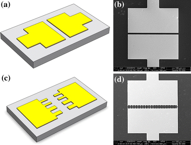
a Schematic of 400-μm-wide electrode design. b SEM image of the fabricated 400-μm-wide electrodes. c Schematic of “teeth”-like electrode design. d SEM image of the fabricated “teeth”-like electrodes
The electrodes are fabricated on 4-inch silicon wafers. The wafers are covered by a 200-nm-thick thermal-grown SiO2 insulating layer. Metal layers of Cr (100 nm, adhesion material) and Au (200 nm, electrode material) are coated on the wafer surface with sputtering. One of the biggest advantages of dielectrophoresis in nanotube alignment is its potential in wafer-level-controlled deposition, which is compatible with the parallel micro/nanofabrication processes used in the semiconductor industry. Therefore, series (and often expensive) nanofabrication processes using equipment such as electron-beam lithography and scanning-probe lithography should be avoided. In our investigation, the entire fabrication process is compatible with the traditional microfabrication technology. We use optical lithography with a hard contact aligner, a positive photoresist (Shipley S1813), and controlled wet etching to obtain electrodes with sharp tips which can dramatically strengthen the local electric field. The parameters for the etching steps are 120 s for Cr etching using a standard chromium mask etchant and 20 s for Au etching using a gold etchant (Type TFA from Transene Inc.). After the controlled etching process, the actual widths of the electrodes are reduced to 2–3 (designed width: 5 μm) and 0.5–1 μm (designed width: 3 μm).
Figure 2a shows the schematic of the experimental system for the dielectrophoresis of SWNTs. A function generator (Agilent Technologies 81150A) is used as the AC signal source, and it is connected to the electrodes through two metal probes. The potential drop across the electrode gap is monitored by an oscilloscope (Agilent Technologies MSO 7054A), which provides the voltage value in real time. After the instruments are set up, a droplet of SWNT solution is carefully placed in the area between the electrodes with a syringe. Next, the AC signal source is switched on; an electric field is generated in between the electrode “teeth”. The electric field exerts a net force on the SWNTs and forces them to rotate along the field line. The SWNTs can be deposited on the substrate with this orientation, as shown in Fig. 2b. After 30 s of dielectrophoresis, the AC signal is switched off, and the SWNT solution is removed with another syringe. The experiments are conducted at room temperature with an applied AC signal with peak-to-peak voltage Vpp = 10 V and frequency f = 5 MHz.
Figure 2.
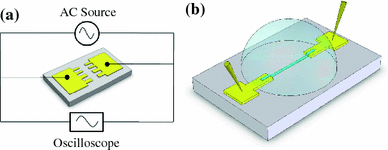
a Experimental system set up. b SWNT alignment configuration
Results and Discussion
Based on the designs of the electrodes, the fabricated devices can be divided into three groups: 400-μm-wide electrodes, 5-μm-wide electrodes, and 3-μm-wide electrodes. For each group, the electrodes are exposed to the SWNT solutions with different concentrations, ranging from 0.2 to 0.0125 mg/ml. An SEM (FEI Quanta 3D 200i) is used to inspect the devices after the dielectrophoresis process. Figure 3 shows the SEM images of the deposited SWNTs on the devices with the 400-μm-wide electrodes. This electrode design enables an eventually distributed electric field with parallel field lines in the gap. The SWNTs are stretched and aligned in between the electrodes to follow the parallel electric field lines. The density of the SWNT thin film is dependent on the concentration of the SWNT solution used in the dielectrophoresis. A higher solution concentration induces a denser SWNT film. The alignment experiments are highly repeatable when used to fabricate SWNT thin films. However, it is difficult to obtain small nanotube bundles or individual nanotubes using this group of devices.
Figure 3.
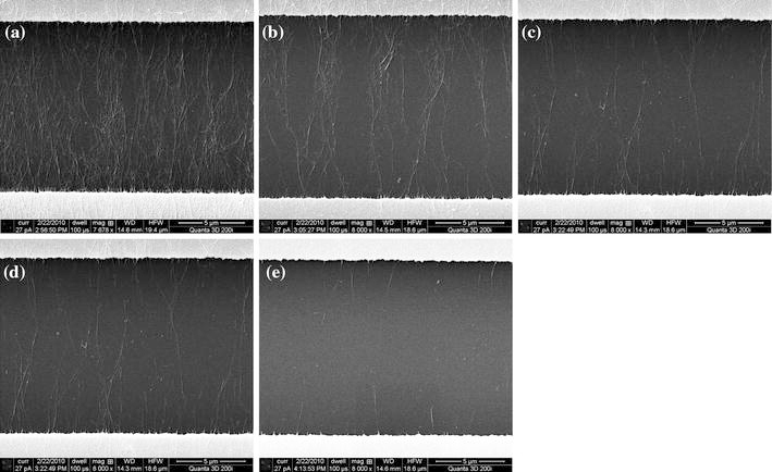
SEM images of aligned SWNTs with 400-μm-wide electrodes and solutions with different concentrations: a 0.2 mg/ml, b 0.1 mg/ml, c 0.05 mg/ml, d 0.025 mg/ml, and e 0.0125 mg/ml
In order to explore the possibility of producing aligned nanotube bundles and individual nanotubes, narrower electrodes are used. Figure 4 shows the SEM images of the aligned SWNTs on the devices with 5-μm-wide electrodes. Figure 4a demonstrates a dense film of SWNTs covering the electrode gap, where most SWNTs are aligned to follow the direction of the electric field lines. As the solution concentration decreases, fewer SWNTs are attracted by the dielectrophoresis force and deposited on the substrate. In addition, there are no SWNTs observed outside the electrode gap area. This proves that the dielectrophoresis process is a selective deposition technique that only moves SWNTs to areas with strong electric fields. Figure 4b–4d show sparsely distributed nanotube bundles and Fig. 4e shows a small bundle of SWNTs. Compared with the devices with wider electrodes (Fig. 3), the devices with 5-μm-wide electrodes can generate a more concentrated electric field in the gap and force the SWNTs to land on the substrate to cover a smaller area. The bundling phenomenon of SWNTs in the solution is caused by their high aspect ratios and high flexibility. By comparing Fig. 4b–4e, as the solution concentration decreases, the bundles become thinner due to the lower availability of SWNTs in the solution.
Figure 4.
SEM images of aligned SWNTs with 5-μm-wide electrodes and solutions with different concentrations: a 0.2 mg/ml, b 0.1 mg/ml, c 0.05 mg/ml, d 0.025 mg/ml, and e 0.0125 mg/ml
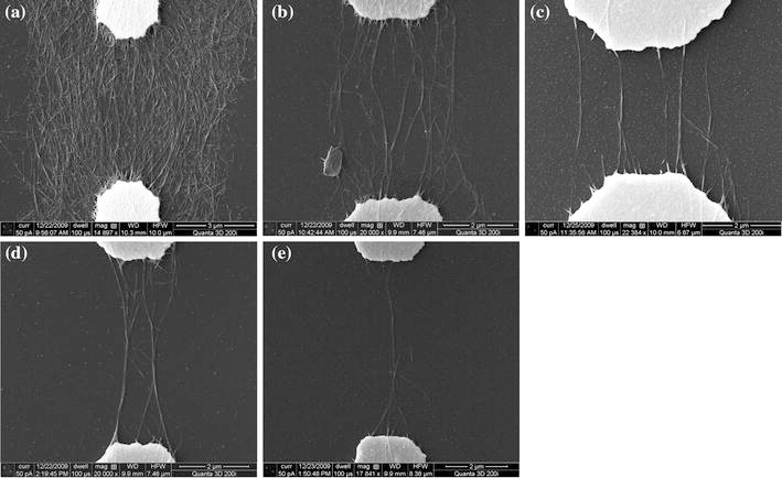
For the narrowest electrodes with 3 μm width, the quality of the deposition and alignment of SWNTs is similar to that for the electrodes with 5 μm width, as shown in Fig. 5. However, there are three major differences comparing the results from the two designs. First, the amount of the aligned SWNTs on the 3-μm-wide electrodes is smaller. This is because the area with strong and concentrated electric field generated by the narrower electrodes is smaller. Second, the bundles deposited on the 3-μm-wide electrodes are thinner and contain smaller numbers of nanotubes. Third and most importantly, individual nanotubes can be observed in the dielectrophoresis experiments using low-concentration solutions and 3-μm-wide electrodes (Fig. 5e). In this case, the narrow electrode design ensures that the electric field in between the electrodes is extremely concentrated and highly directional. The low solution concentration ensures that in the adjacent area there is only one nanotube available in the solution to be attracted by the electric field. Consequently, this individual nanotube is deposited on the substrate and aligned in between the electrodes.
Figure 5.
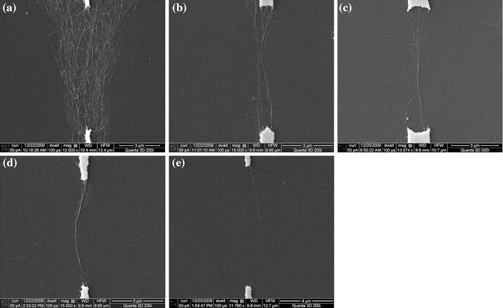
SEM images of aligned SWNTs with 3-μm-wide electrodes and solutions with different concentrations: a 0.2 mg/ml, b 0.1 mg/ml, c 0.05 mg/ml, d 0.025 mg/ml, and e 0.0125 mg/ml
To gain a better understanding of the solution concentration effect on the dielectrophoresis process, the electrical properties of the devices after dielectrophoresis are characterized with a semiconductor device analyzer (Agilent Technologies B1500A). All the devices are based on the second electrode design which contains the “teeth”-like electrodes with variable widths (Fig. 1d). Each device consists of eleven 5-μm-wide electrode pairs and nine 3-μm-wide electrode pairs. Figure 6a shows the current–voltage (I–V) plots of five devices using SWNT solutions with five different concentrations. In the measured range between −3 and 3 V, all five I–V plots are highly linear. The resistances of these devices are calculated based on the I–V characterization and plotted in Fig. 6b. At a low SWNT solution concentration of 0.0125 mg/ml, the resistance is measured as approximately 11 kΩ. As the concentration increases, the resistance quickly decreases to a lower value. The characterization of these devices verifies the results from the SEM inspection and proves that higher-concentration solutions lead to denser films with more deposited SWNTs. The high linearity of the I–V plots suggests that the aligned SWNTs are mostly metallic nanotubes instead of semiconducting nanotubes. These experimental results fit well with the prediction described in the Dielectrophoresis part.
Figure 6.
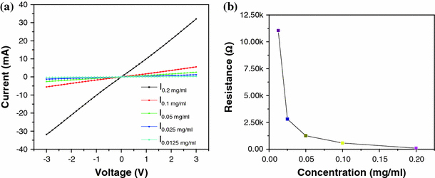
a Current–voltage plots of five devices using SWNT solutions with different concentrations. b Resistances calculated from a
The selective deposition and alignment of nanotube bundles and individual nanotubes are highly repeatable. This method can be used in the development of individual nanotube devices and systems. This may give nanotube-based electronics a wide range of new opportunities. For example, in addition to the traditional electronic applications as field-effect transistors and circuits, devices with a controlled amount of SWNTs can be used as high-performance sensors for chemical sensing, gas detection, and DNA analysis. Even though the fabrication and deposition steps presented in this paper are still used for small-scale processes, they can be easily extended to large-scale production. Furthermore, because the entire process is compatible with the traditional microfabrication technology, it has a high potential to be used in wafer-level fabrication to produce identical devices across the entire surface of the substrate.
Conclusions
In conclusion, we have successfully deposited and aligned nanotube thin films, small bundles, and individual nanotubes at desired locations. The different alignment results are achieved by using various electrode designs and SWNT solutions with various concentrations. In general, electrodes with large widths (400 and 5 μm) generate an eventually distributed electric field with parallel field lines; the aligned SWNTs are in the form of thin films or sparsely distributed bundles. For electrodes with small width (3 μm), the electric field is highly concentrated and can induce individual nanotube deposition and alignment. The electrical characterization shows that the aligned SWNTs have a highly linear current–voltage relationship, which proves that the aligned SWNTs are mostly metallic nanotubes. In addition, the fabrication process is compatible with the traditional microfabrication technology and has a high potential to be used in the wafer-level fabrication in the future. The method presented in this paper can be used in a wide range of applications, especially in the development of individual nanotube-based devices.
Acknowledgments
This work was supported by the Washington State University New Faculty Seed Grant (award ID: 110300_001).
Open Access
This article is distributed under the terms of the Creative Commons Attribution Noncommercial License which permits any noncommercial use, distribution, and reproduction in any medium, provided the original author(s) and source are credited.
References
- Rao CNR, Satishkumar BC, Govindaraj A, Nath M. Chemphyschem. 2001. p. 78. COI number [1:CAS:528:DC%2BD3MXhs12rs78%3D] [DOI] [PubMed]
- Boul PJ, Turner K, Li J, Pulikkathara MX, Dwivedi RC, Sosa ED, Lu Y, Kuznetsov OV, Moloney P, Wilkins R, O’Rourke MJ, Kliabashesku VN, Arepalli S, Yowell L. J. Phys. Chem. C. 2009. p. 14467. COI number [1:CAS:528:DC%2BD1MXovVelsLs%3D] [DOI]
- Wang Y, Zhou Z, Yang Z, Chen X, Xu D, Zhang Y. Nanotechnology. 2009. p. 345502. [DOI] [PubMed]
- Xue W, Cui T. Sens. Actuators B. 2008. p. 981. [DOI]
- Xue W, Liu Y, Cui T. Appl. 2006. p. 163512. Bibcode number [2006ApPhL..89p3512X] [DOI]
- Hu P, Zhang C, Fasoli A, Scardaci V, Pisana S, Hasan T, Robertson J, Milne WI, Ferrari AC. Physica E. 2008. p. 2278. COI number [1:CAS:528:DC%2BD1cXmt1Onu7g%3D]; Bibcode number [2008PhyE...40.2278H] [DOI]
- Robertson J, Zhong G, Telg H, Thomsen C, Warner JH, Briggs GAD, Dettlaff-Weglikowska U, Roth S. Appl. 2008. p. 163111. Bibcode number [2008ApPhL..93p3111R] [DOI]
- Chen Z, Yang Y, Chen F, Qing Q, Wu Z, Liu Z. J. Phys. Chem. B. 2005. p. 11420. COI number [1:CAS:528:DC%2BD2MXktF2rtrk%3D] [DOI] [PubMed]
- Hu L, Choi JW, Yang Y, Jeong S, La Mantia F, Cui LF, Cui Y. PNAS. 2009. p. 21490. COI number [1:CAS:528:DC%2BC3cXltlGktQ%3D%3D]; Bibcode number [2009PNAS..10621490H] [DOI] [PMC free article] [PubMed]
- Kaempgen M, Chan CK, Ma J, Cui Y, Gruner G. Nano Lett. 2009. p. 1872. COI number [1:CAS:528:DC%2BD1MXktFeltL4%3D]; Bibcode number [2009NanoL...9.1872K] [DOI] [PubMed]
- Li S, Liu N, Chan-Park MB, Yan Y, Zhang Q. Nanotechnology. 2007. p. 455302. Bibcode number [2007Nanot..18S5302L] [DOI]
- Liu H, Takagi D, Chiashi S, Homma Y. Nanotechnology. 2009. p. 345604. [DOI] [PubMed]
- Tsukruk VV, Ko H, Peleshanko S. Phys. 2004. p. 065502. Bibcode number [2004PhRvL..92f5502T] [DOI] [PubMed]
- LeMieux MC, Roberts M, Barman S, Jin YW, Kim JM, Bao Z. Science. 2008. p. 101. COI number [1:CAS:528:DC%2BD1cXnvFeks7g%3D]; Bibcode number [2008Sci...321..101L] [DOI] [PubMed]
- Roberts ME, LeMieux MC, Sokolov AN, Bao Z. Nano Lett. 2009. p. 2526. COI number [1:CAS:528:DC%2BD1MXmvVCis7g%3D]; Bibcode number [2009NanoL...9.2526R] [DOI] [PubMed]
- Shim JS, Yun YH, Rust MJ, Do J, Shanov V, Schulz MJ, Ahn CH. Nanotechnology. 2009. p. 325607. [DOI] [PubMed]
- Gultepe E, Nagesha D, Casse BDF, Selvarasah S, Busnaina A, Sridhar S. Nanotechnology. 2008. p. 455309. Bibcode number [2008Nanot..19S5309G] [DOI] [PubMed]
- Mureau N, Mendoza E, Silva SRP, Hoettges KF, Hughes MP. Appl. 2006. p. 243109. Bibcode number [2006ApPhL..88x3109M] [DOI]
- Xiao Z, Camino FE. Nanotechnology. 2009. p. 135205. COI number [1:STN:280:DC%2BD1Mzis1CktQ%3D%3D]; Bibcode number [2009Nanot..20m5205X] [DOI] [PubMed]
- Stokes P, Khondaker SI. Nanotechnology. 2008. p. 175202. Bibcode number [2008Nanot..19q5202S] [DOI] [PubMed]
- Monica AH, Papadakis SJ, Osianderd R, Paranjape M. Nanotechnology. 2008. p. 085303. Bibcode number [2008Nanot..19h5303M] [DOI] [PubMed]
- Yuen FL-Y, Zak G, Waldman SD, Docoslis A. Cytotechnology. 2008. p. 9. [DOI] [PMC free article] [PubMed]
- Zhou R, Wang P, Chang HC. Electrophoresis. 2006. p. 1376. COI number [1:CAS:528:DC%2BD28Xjslyltbw%3D] [DOI] [PubMed]
- Lim JH, Phiboolsirichit N, Mubeen S, Deshusses MA, Mulchandani A, Myung NV. Nanotechnology. 2010. p. 075502. Bibcode number [2010Nanot..21g5502L] [DOI] [PubMed]
- Di Bartolomeo A, Rinzan M, Boyd AK, Yang Y, Guadagno L, Giubileo F, Barbara P. Nanotechnology. 2010. p. 115204. Bibcode number [2010Nanot..21k5204D] [DOI] [PubMed]
- Padmaraj D, Zagozdzon-Wosik W, Xie LM, Hadjiev VG, Cherukuri P, Wosik J. Nanotechnology. 2009. p. 035201. COI number [1:STN:280:DC%2BD1MzitlKktg%3D%3D]; Bibcode number [2009Nanot..20c5201P] [DOI] [PubMed]
- Dimaki M, Boggild P. Nanotechnology. 2004. p. 1095. COI number [1:CAS:528:DC%2BD2cXnvFKjt7k%3D]; Bibcode number [2004Nanot..15.1095D] [DOI]
- Seo HW, Han CS, Choi DG, Kim KS, Lee YH. Microelectron. 2005. p. 83. COI number [1:CAS:528:DC%2BD2MXlvFantbc%3D] [DOI]
- Peng N, Zhang Q, Li J, Liu N. J. 2006. p. 024309. Bibcode number [2006JAP...100b4309P] [DOI]
- Raychaudhuri S, Dayeh SA, Wang D, Yu ET. Nano Lett. 2009. p. 2260. COI number [1:CAS:528:DC%2BD1MXlsVGqs7Y%3D]; Bibcode number [2009NanoL...9.2260R] [DOI] [PubMed]
- Ahmed W, Kooij ES, van Silfhout A, Poelsema B. Nano Lett. 2009. p. 3786. COI number [1:CAS:528:DC%2BD1MXhtVKksb7M] [DOI] [PubMed]
- Xue W, Cui T. Nanotechnology. 2007. p. 145709. Bibcode number [2007Nanot..18n5709X] [DOI]
- Rinzler AG, Liu J, Dai H, Nikolaev P, Huffman CB, Rodriguez-Macias FJ, Boul PJ, Lu AH, Heymann D, Colbert DT, Lee RS, Fischer JE, Rao AM, Eklund PC, Smalley RE. Appl. Phys. A. 1998. p. 29. COI number [1:CAS:528:DyaK1cXktFKrs7g%3D]; Bibcode number [1998ApPhA..67...29R] [DOI]


