Abstract
In this work, we investigated the use of 10-layer InAs quantum dot (QD) as active region of an electroabsorption modulator (EAM). The QD-EAM is a p-i-n ridge waveguide structure with intrinsic layer thickness of 0.4 μm, width of 10 μm, and length of 1.0 mm. Photocurrent measurement reveals a Stark shift of ~5 meV (~7 nm) at reverse bias of 3 V (75 kV/cm) and broadening of the resonance peak due to field ionization of electrons and holes was observed for E-field larger than 25 kV/cm. Investigation at wavelength range of 1,300–1320 nm reveals that the largest absorption change occurs at 1317 nm. Optical transmission measurement at this wavelength shows insertion loss of ~8 dB, and extinction ratio of ~5 dB at reverse bias of 5 V. Consequently, methods to improve the performance of the QD-EAM are proposed. We believe that QDs are promising for EAM and the performance of QD-EAM will improve with increasing research efforts.
Keywords: InAs quantum dots, Electroabsorption modulator, Ridge waveguide structure, Photocurrent, Optical transmission
Introduction
Semiconductor quantum dots (QDs) is attracting tremendous research interests due to the benefits promised by the three-dimensional (3D) carrier confinement of the QD system. For example, the 3D carrier confinement provides QD lasers the possibilities to achieve low threshold current density and high differential gain. Consequently, high power, efficiency, and temperature insensitivity have been reported [1-3]. Furthermore, the optical properties and surface morphology of the QDs can be tuned by altering the growth process [4,5], rendering this material system suitable for many photonic devices. However, while vast efforts have been channeled to investigate QD photonic devices in optical fiber communication systems, existing research efforts mainly focus on the potential of QDs for transmitters [6-8] and amplifiers [9].
In fact, the 3D carrier confinement of the QDs also results in stronger Coulombic interaction and oscillator strength of the electron-hole pairs as compared to the higher dimensional systems, e.g. quantum wells (QWs) [10]. This property is attractive for electroabsorption modulators (EAMs) utilizing the QD systems since it theoretically implies higher efficiency as compared to the QW counterparts, i.e. larger extinction ratio (ER) for a given external electric field (Fext) or lower Fext for a given ER [11]. However, to date, there are little research efforts on the investigation of QDs for EAMs. Furthermore, most of the existing works discuss either the quantum confined Stark effect (QCSE) [12,13] or carriers dynamics [12,14] of QDs under reverse bias.
Motivated by the abovementioned possibility of achieving EAMs with higher efficiency, we investigate the potential of employing semiconductor QDs as the active region for EAMs. In this work, we will report on the photocurrent (PC) and optical transmission measurement of the EAM device which consists of 10-layer InAs QDs as the active region, i.e. QD-EAM.
Experimental Procedure
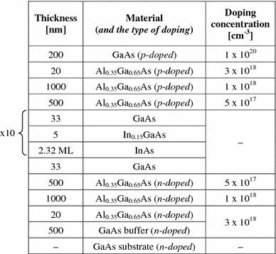
Figure 1 depicts the layer structure of the InAs QD-EAM under investigation. The epitaxial layers were grown using solid-source molecular beam epitaxy (SS-MBE) on n-doped GaAs (100) substrates. As shown in the figure, the repeated layers consist of 2.32 monolayer (ML) of InAs coverage, 5 nm-thick In0.15Ga0.85As, and 33 nm-thick GaAs. The In0.15Ga0.85As acts as strain-reducing layer (SRL) to tune the emission/absorption wavelength toward 1.3 μm [15], while the GaAs acts as spacer layer to decouple the strain effect of the QD layers [16].
Figure 1.

Layer structure of the InAs QD-EAM under investigation. The QD monolayer (ML) coverage is also included
The QD wafer was processed into ridge waveguide (WG) structure with 10 μm ridge width by standard wet chemical etching. Both p-type and n-type ohmic contacts layers were deposited by electron beam evaporation, and the backside of the substrate was lapped to ~100 μm prior to the n-metallization process. The wafer was then annealed at 410 °C for 3 min in N2 ambient before cleaving into QD-EAM devices of 1 mm cavity length. Further details of the fabrication process can be found elsewhere [17].
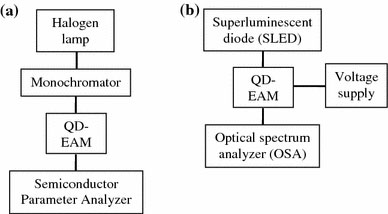
Figure 2a and b depicts the setup used for PC and optical transmission measurements, respectively. The PC measurement setup consists of a monochromated broadband light source incident onto the front facet of the WG QD-EAM device, and voltage-dependent (0 to −3 V) photocurrent is extracted with the use of the semiconductor parameter analyzer (HP/Agilent 4156B). The optical transmission measurement setup consists of a superluminescent diode (SLED) incident onto the front facet of the WG QD-EAM, with transmitted power at the back facet detected by an optical spectrum analyzer (OSA). Both the front and back facets of the WG QD-EAM are as-cleaved and reverse bias of 0–5 V is controlled by a DC voltage supply. The fibers used are 9 μm core-diameter single-mode fibers with cleaved facets. All measurements are conducted at room temperature.
Figure 2.

Schematic view of the setup used foraphotocurrent andboptical transmission measurements of the QD-EAM
Results and Discussion
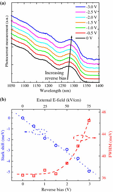
Figure 3a depicts the voltage-dependent PC spectra. As verified from the photoluminescence spectra (not shown), the lowest resonance peak at ~1280–1300 nm is due to absorption by the QD ground state transition. Recognizing that the bandgap of In0.15Ga0.85As strain-reducing layer is ~1.265 eV (~980 nm) [18], we believed that the sub-bandgap absorptions at 1100 nm and 1175 nm are due to the first and second excited states of the InAs QDs, respectively. Figure 3b depicts the voltage-dependent Stark shift and full-width at half-maximum (FWHM) of the resonance peaks. The values were obtained from Gaussian fittings of the PC resonance peaks. The externally applied electric field (E-field) is calculated by assuming an intrinsic layer thickness of approximately 0.4 μm.
Figure 3.

aVoltage-dependent photocurrent (PC) measurement across 0.4 µm intrinsic region. The PC spectra are offset vertically for clarity.bVoltage-dependent Stark shift and full-width at half-maximum (FWHM) of the resonance peaks in (a). The dotted and dashed lines provide guides for the eyes
One can see that the shift of the absorption peak (i.e. Stark shift) is ~3.3 meV (~4.7 nm) at applied reverse bias of 2 V (50 kV/cm). Compared with the QW counterpart, this shift is approximately half the value of a 10 nm wide square QW [19]. However, this is typical for QDs since the shift depends strongly on the dimension of the confinement along the applied E-field, and is therefore smaller as the QD height is typically less than 10 nm [20,21]. It is to be noted that the straight dotted line only serves as guide to the eyes and does not imply that the Stark shift follows a linear behavior. In fact, both theoretical studies and experimental results had confirmed that QDs exhibit a quadratic relation with the E-field [21,22]. Therefore, similar to that reported in Fig. 3 (for sample D) of Ref. [21], the data appear linear because the range of E-field considered is only 75 kV/cm, and it is far from the maximum point of the quadratic curve. Furthermore, for applied E-field greater than 25 kV/cm, one can also see the broadening of the peak. This is due to field ionization of electrons and holes with increasing E-field [23].
Due to the lack of inversion symmetry as a result of their asymmetric shape, QDs are expected to have a permanent dipole moment. This implies that the electron center of mass should be displaced with respect to the hole center of mass and thus, the Stark shift will not have a maximum point at zero E-field. However, it is interesting to highlight that while earlier theoretical work [24-27] based on InAs QDs with perfect pyramidal shape and uniform composition suggests that the electron wave function is localized above that of the hole, recent photocurrent measurements performed by Fry et al. [21] shows otherwise. This implies that the maximum point of the Stark shift actually lies on the negative E-field, i.e. on the left side of the vertical axis—it is worth mentioning that, as seen from Fig. 3b, our results agree with that of Ref. [21]. As verified experimentally and theoretically [28,29], this is due to actual QDs having a truncated pyramidal shape and a non-zero and non-uniform Ga composition within the dots.
Note that PC measurement can be employed to investigate both the quantum confined Stark effect (QCSE) and field-dependent absorption changes of the active region [30]. However, extraction of the absorption spectra is more relevant for EAM employing the surface-normal structure where 100% quantum efficiency is normally assumed. Therefore, only the former is presented in this work since the accuracy of the absorption spectra for WG structure will depend on the knowledge of the coupling coefficient and intrinsic propagation loss.
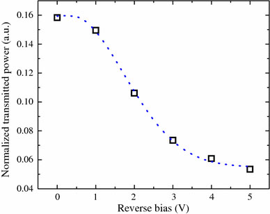
By considering the technologically important wavelength range of 1,300–1,320 nm [31], we consider the normalized transmitted power versus reversed bias curves for wavelength in steps of 1 nm. This gives a total of 21 curves, and the wavelength that gives the largest change in transmission is then determined, i.e. 1,317 nm in this work. The normalized transmitted power as function of the reverse bias at 1,317 nm is thus presented in Fig. 4. The normalized transmitted power of 1.0 is defined as the free-space coupling of the SLED to the OSA, i.e. the absence of the QD-EAM in Fig. 2b.
Figure 4.

Normalized transmitted power as a function of reverse bias. The result was obtained for the wavelength of 1317 nm. The dotted line provides guide for the eyes
The insertion loss, which consists of reflection, propagation, and mode coupling losses, is defined as  and is ~8 dB. This value is higher than that reported (~3.0–4.5 dB) for EAMs with anti-reflection (AR) coating [32,33]. Since reflection loss accounts for ~3 dB of the insertion loss [34], introducing AR coatings on both the front and back facets of our device will reduce the insertion loss to ~5 dB and make our insertion loss comparable to theirs. As seen from the ~1,280 nm resonant peak of the 0 V photocurrent signal in Fig. 3a, the absorption profile extends to ~1,340 nm. Hence, the residual absorption loss (and consequently, the propagation loss) of our QD-EAM cannot be ignored since the signal wavelength of 1,317 nm still lies within the absorption profile. One method to reduce the residual absorption loss is to blueshift the resonance peak and its absorption profile, i.e. by having a larger detuning energy. Since the electronic properties of the quantum dots (QDs) depend on its size, shape, and surrounding matrix [35], this can be done by reducing the indium composition of the InGaAs SRL [15]. While mode coupling loss cannot be eliminated due to the large difference between the fiber and active region dimensions of the WG QD-EAM, it can be optimized through proper waveguide design [34].
The extinction ratio (ER) is defined as  and is ~5 dB at a reverse bias of 5 V for our QD-EAM device. This result is encouraging since pioneering works on QW-EAM require reverse bias of 12 V for a double GaAs/AlGaAs QW structure [36] and 11 V for an 80-layer InGaAs/InP QW structure [32] to achieve the same magnitude of extinction ratio (i.e. 5 dB). While the obtained value is still smaller than the minimum acceptable value of 10 dB for practical applications, this performance can be improved by increasing the number of QD layers. Therefore, by applying AR coatings to both the WG facets, blueshifting the resonance peak such that the signal wavelength lies at the edge of the absorption profile, and increasing the number of QD layers, better performance can be expected from EAMs utilizing the QD system.
Conclusion
In summary, we report the preliminary results of a QD-EAM consisting of 10-layer InAs QDs as active region. The QD-EAM is a p-i-n ridge waveguide structure with intrinsic layer thickness, ridge width, and length of 0.4 μm, 10 μm, and 1.0 mm, respectively. The Stark shift was found to be ~5 meV (~7 nm) at reverse bias of 3 V (75 kV/cm) and broadening of the resonance peak due to field ionization of electrons and holes was observed for E-field larger than 25 kV/cm. Investigation at wavelength range of 1,300–1,320 nm reveals that the largest absorption change occurs at 1,317 nm. Extinction ratio at 1,317 nm was ~5 dB at reverse bias of 5 V. This result is encouraging as compared to pioneering works on QW EAM where reverse bias of more than 10 V is required to achieve the same change in the extinction ratio. Insertion loss was found to be ~8 dB and methods to reduce the various components of the insertion loss were discussed. Furthermore, methods to improve the performance of the QD-EAM are proposed. We believe that QDs are promising for EAM and the performance of QD-EAM will improve with increasing research efforts.
Acknowledgments
The authors would like to thank Dr. Yang Hua for the valuable advice on the optical transmission measurement setup. This project is partially supported by the DSTA Defense Innovative Research Project (POD0613635). One of the authors (C. Y. Ngo) would like to acknowledge the financial support from the A*STAR Graduate Scholarship program.
References
- Mikhrin SS, Kovsh AR, Krestnikov IL, Kozhukohov AV, Livshits DA, Ledentsov NN, Shernyakov YM, Novikov II, Maximov MV, Ustinov VM, Alferov ZI. Semicond. 2005. p. 340. COI number [1:CAS:528:DC%2BD2MXlt1yhtLc%3D] [DOI]
- Shchekin OB, Deppe DG. IEEE Photon Technol. 2002. p. 1231. [DOI]
- Kovsh AR, Maleev NA, Zhukov AE, Mikhrin SS, Vasil’ev AP, Shernyakov YM, Maximov MV, Livshits DA, Ustinov VM, Alferov ZI, Ledentsov NN, Bimberg D. Electron. 2002. p. 1104. COI number [1:CAS:528:DC%2BD38XoslWjtLw%3D] [DOI]
- Ngo CY, Yoon SF, Fan WJ, Chua SJ. Appl. 2007. p. 113103. [DOI]
- Ngo CY, Yoon SF, Tong CZ, Loke WK, Chua SJ. Nanotechnology. 2007. p. 365708. [DOI]
- Ledentsov NN, Bimberg D, Hopfer F, Mutig A, Shchukin VA, Savel’ev AV, Fiol G, Stock E, Eisele H, Dähne M, Gerthsen D, Fischer U, Litvinov D, Rosenauer A, Mikhrin SS, Kovsh AR, Zakharov ND, Werner P. Nanoscale Res. 2007. p. 417. COI number [1:CAS:528:DC%2BD2sXhtl2rtrnM] [DOI] [PMC free article] [PubMed]
- Yoon SF, Liu CY, Sun ZZ, Lew KC. Nanoscale Res. 2006. p. 20. [DOI]
- Yoo YC, Han IK, Lee JI. Electron. 2007. p. 17.
- Akiyama T, Sugawara M, Arakawa Y. Proc. IEEE. 2007. p. 175. [DOI]
- Susa N. J. 1996. p. 1760. COI number [1:CAS:528:DyaK28XmtVaqs7s%3D] [DOI]
- Qasaimeh O, Kamath K, Bhattacharya P, Phillips J. Appl. 1998. p. 1275. COI number [1:CAS:528:DyaK1cXhsl2kt70%3D] [DOI]
- Malins DB, Gomez-Iglesias A, Spencer P, Clarke E, Murray R, Miller A. Electron. 2007. p. 12. [DOI]
- Ohmori M, Torii K, Sakaki H. Phys. Status Solidi C. 2006. p. 512. COI number [1:CAS:528:DC%2BD28XislOqsb8%3D] [DOI]
- Chang WH, Hsu TM, Huang CC, Hsu SL, Lai CY, Yeh NT, Nee TE, Chyi JI. Phys. Rev. B. 2000. p. 6959. COI number [1:CAS:528:DC%2BD3cXmsFShtLk%3D] [DOI]
- Seravalli L, Minelli M, Frigeri P, Allegri P, Avanzini V, Franchi S. Appl. 2003. p. 2341. COI number [1:CAS:528:DC%2BD3sXis1Oktr4%3D] [DOI]
- Howe P, Le Ru EC, Clarke E, Murray R, Jones TS. J. 2005. p. 113511. [DOI]
- Cao Q, Yoon SF, Liu CY, Ngo CY. Nanoscale Res. 2007. p. 303. COI number [1:CAS:528:DC%2BD2sXpslegsbY%3D] [DOI]
- Tong CZ, Yoon SF, Ngo CY, Liu CY, Loke WK. IEEE J. 2006. p. 1175. COI number [1:CAS:528:DC%2BD28XhtlWgu7%2FL] [DOI]
- Li EH, Chan KS, Weiss BL, Micallef J. Appl. 1993. p. 533. COI number [1:CAS:528:DyaK3sXls12mtr4%3D] [DOI]
- Lee SJ, Kim JO, Noh SK, Choe JW, Lee KS. J. Cryst. Growth. 2005. p. 39. COI number [1:CAS:528:DC%2BD2MXhtVartbzM] [DOI]
- Fry PW, Itskevich IE, Mowbray DJ, Skolnick MS, Finley JJ, Barker JA, O’Reilly EP, Wilson LR, Larkin IA, Maksym PA, Hopkinson M, Al-Khafaji M, David JPR, Cullis AG, Hill G, Clark JC. Phys. 2000. p. 733. COI number [1:CAS:528:DC%2BD3cXlvVKmug%3D%3D] [DOI] [PubMed]
- Sheng W, Leburton JP. Phys. Rev. B. 2001. p. 161301. [DOI]
- Miller DAB, Chemla DS, Damen TC, Gossard AC, Wiegmann W, Wood TH, Burrus CA. Phys. Rev. B. 1985. p. 1043. COI number [1:CAS:528:DyaL2MXkslymtbs%3D] [DOI] [PubMed]
- Grundmann M, Stier O, Bimberg D. Phys. Rev. B. 1995. p. 11969. COI number [1:CAS:528:DyaK2MXptVSqtr0%3D] [DOI] [PubMed]
- Cusack M, Briddon PR, Jaros M. Phys. Rev. B. 1996. p. R2300. COI number [1:CAS:528:DyaK28XkslWjsbc%3D] [DOI] [PubMed]
- Pryor C. Phys. Rev. B. 1998. p. 7190. COI number [1:CAS:528:DyaK1cXhvVejsb8%3D] [DOI]
- Kim J, Wang LW, Zunger A. Phys. Rev. B. 1998. p. R9408. COI number [1:CAS:528:DyaK1cXisVGgu7o%3D] [DOI]
- Kegel I, Metzger TH, Lorke A, Peisl J, Stangl J, Bauer G, García JM, Petroff PM. Phys. 2000. p. 1694. COI number [1:CAS:528:DC%2BD3cXlslGntLw%3D] [DOI] [PubMed]
- Barker JA, O’Reilly EP. Phys. Rev. B. 2000. p. 13840. COI number [1:CAS:528:DC%2BD3cXjs1Smtb8%3D] [DOI]
- Jalili YS, Stavrinou PN, Roberts JS, Parry G. Electron. 2002. p. 343. COI number [1:CAS:528:DC%2BD38XjtlWis78%3D] [DOI]
- Loi KK, Shen L, Wieder HH, Chang WSC. IEEE Photon Technol. 1997. p. 1229. [DOI]
- Koren U, Miller BI, Koch TL, Eisenstein G, Tucker RS, Bar-Joseph I, Chemla DS. Appl. 1987. p. 1132. COI number [1:CAS:528:DyaL2sXmtVynt7c%3D] [DOI]
- Rolland C, Mak G, Prosyk KL, Maritan CM, Puetz N. IEEE Photon Technol. 1991. p. 894. [DOI]
- Chin MK, Chang WSC. IEEE J. 1993. p. 2476. COI number [1:CAS:528:DyaK2cXhslOnu7Y%3D] [DOI]
- Ngo CY, Yoon SF, Fan WJ, Chua SJ. Phys. Rev. B. 2006. p. 245331. [DOI]
- Wood TH, Burrus CA, Tucker RS, Weiner JS, Miller DAB, Chemla DS, Damen TC, Gossard AC, Wiegmann W. Electron. 1985. p. 693. COI number [1:CAS:528:DyaL2MXltFeisL0%3D] [DOI]


