Abstract
A fast and cost-effective technique is applied for fabricating cobalt and nickel nanopillars on aluminium substrates. By applying an electrochemical process, the aluminium oxide barrier layer is removed from the pore bottom tips of nanoporous anodic alumina templates. So, cobalt and nickel nanopillars are fabricated into these templates by DC electrodeposition. The resulting nanostructure remains on the aluminium substrate. In this way, this method could be used to fabricate a wide range of nanostructures which could be integrated in new nanodevices.
Keywords: Nanoporous anodic alumina membranes, Transfer mask, Metallic nanopillars, Electrodeposition
Introduction
The template synthesis of nanostructures has attracted scientists’ attention in the last years owing to their possible application in fabricating high-density magnetic storage memories [1] and nanoelectrodes for electrochemical processes in nanometric range [2]. In addition, this kind of nanostructures could be integrated in smaller and smaller devices such as filters [3] or sensors [4]. In terms of nanostructure fabrication, choosing a suitable template is one of the most crucial factors in the synthesis process, because any defect in the template structure could be transferred to the resulting nanostructure by replication. So far, several materials have been used as template for synthesizing nanowires or nanotubes. Nanoporous anodic alumina membranes (NAAMs) have become widely used for the following reasons: first, in contrast to other membranes as polycarbonate membranes, NAAMs present a higher pore density and a narrower diameter pore distribution [5]. Secondly, both the pore diameter and their interpore distance are rather controllable, because they can be adjusted by varying the anodization voltage or changing the electrolyte [6]. Thirdly, by means of a two-step anodization process [7], we can fabricate NAAMs with a self-ordered hexagonally and periodic pore arrangement in a more inexpensive way than with other methods like electron beam lithography [8]. Recently, electrochemical deposition from an electrolyte has been used [9,10], since it is a fast and well-controlled way of fabricating nanowires and nanotubes by filling porous templates. Nonetheless, as-produced NAAMS have certain disadvantages to be used as template when an electrochemical deposition is desirable. The main disadvantage is that there is an aluminium oxide (Al2O3) barrier layer between the pore bottom and the aluminium (Al) substrate. This barrier layer electrically isolates the metallic aluminium substrate from the inner side of the pores. For this reason, when an electrodeposition of a metallic or semiconducting material is carried out by direct current (DC) in an as-produced NAAM, it is rather unstable and there is no uniform filling of the pores. Moreover, high electrodeposition potentials are needed for tunnelling the electrons throughout the oxide barrier layer of the pore bottom. Other deposition techniques like electroless deposition [11], chemical vapour deposition (CVD) [12] or sol–gel [13] can avoid this drawback, since the growth of nanowires or nanotubes does not start at the pore tips, but from the pore walls. So far, several methods have been developed for carrying an electrochemical deposition using NAAMs as template. The most commonly used are two. In the first one [9,10], the nanoporous alumina membrane must be detached from the aluminium substrate by the dissolution of the Aluminium in a saturated solution of cupric chloride and hydrochloric acid (HCl·CuCl2) [14] or in a saturated solution of mercury (II) chloride (HgCl2) [15]. Subsequently, the aluminium oxide barrier layer is removed from the pore bottoms by a chemical etching process in a solution of phosphoric acid (H3PO4). Finally, an electrical contact is sputtered on one side of the free-standing NAAM. The second one is the pulsed electrodeposition (PED) method [16], in which the NAAM remains on the aluminium substrate. By means of this method, magnetic nanowire arrays of nickel and cobalt have been fabricated [16,17]. Nevertheless, only free-standing metallic nanowires can be fabricated using this method.
In this work, we present an innovative method for fabricating cobalt (Co) and nickel (Ni) nanopillars (NPs) on aluminium substrates. In contrast to previous works [16,17], the metallic nanowires remain on the aluminium substrate after removing the alumina template. Recently, we have used a technique, previously developed by ourselves, for dissolving in situ the aluminium oxide barrier layer on the pore bottom tips of NAAMs [18]. We describe the experimental procedure to fabricate Co and Ni nanopillars as follows: first, we explain the technique used to achieve the aluminium oxide barrier layer dissolution. Secondly, we describe the DC electrochemical deposition process. Thirdly, we show and discuss the results of the template synthesis method presented, and finally we present our conclusions.
Experimental
Fabrication of Nanoporous Anodic Alumina Membrane
Hexagonally ordered home-made NAAMs were prepared using direct anodization of aluminium substrates, which is described in detail somewhere else [19,20]. First, commercial aluminium substrates (high-purity aluminium [99.999%] foils from Goodfellow Cambridge Ltd) were pre-treated. The aluminium foils were annealed in nitrogen (N2) environment at 400 °C for 3 h. In this way, both their crystalline phase and grain size were homogenized. Subsequently, samples were electropolished in a mixture of ethanol (EtOH) and perchloric acid (HClO4) 4:1 (v:v) to reduce their surface roughness. Finally, the samples were washed with deionized water, dried under a draught and stored in a dry environment to prevent the formation of oxide thin films because of environmental humidity. Once the aluminium foils were pre-treated, the anodization process was carried out following an innovative electrochemical approach for dissolving in situ the aluminium oxide barrier layer on the pore bottom tips of the NAAMs [18]. The two-step hard anodization (HA) procedure was performed on the aluminium surface using an oxalic acid (H2C2O4) solution (0.3 M) at 0 °C in order to prevent the oxide film burning by catastrophic electric current flow. The first stage of the anodization process was started under constant voltage at 40 V for 5 min. So, a protective thin layer about 0.5 μm thick was formed on the aluminium surface. This layer suppresses breakdown effects due to high temperature and enables uniform oxide film growth at high voltage. Subsequently, the voltage was slowly increased to the HA anodization voltage (120 V) at a constant rate of 0.8 V s−1. The voltage was then maintained constant for 20 min in order to achieve a suitable hexagonal arrangement of the pores. When the first anodization stage finished, the aluminium oxide film was removed from the aluminium substrate by wet chemical etching in a mixture of phosphoric acid (H3PO4) (0.4 M) and chromic acid (H2Cr2O7) (0.2 M) at 70 °C during the same time of the first anodization stage (about 30 min). In this way, we produced a pre-pattern on aluminium surface. Afterwards, the second stage of the anodization process consisted of directly applying an anodizing voltage of 120 V in the same electrolyte in which the first stage was carried out. The anodization voltage was maintained until the desired pore depth had been reached (around 10 min). Previous studies have found that the rate of film growth is nonlinear [19], being approximately between 50 and 70 μm h−1. The third stage of the anodization process is initiated, applying a stepwise current-limited re-anodization procedure under a galvanostatic regime in the same electrolyte. In this way, the aluminium oxide barrier layer of the pore bottom tips of the NAAMs was penetrated. In this step, the previous value of the current density was halved, and the sample was re-anodized. Then, the voltage fell until it reached a quasi-steady value. When this almost steady state had been reached, the current density was again halved and the voltage decreased again. So, the thickness of the oxide barrier layer was reduced several tens of nanometres in each re-anodization step. By means of consecutive repetitions of this procedure, the oxide barrier layer was penetrated without the NAAM detachment from the aluminium substrate. Finally, since the aluminium oxide barrier layer is not uniform in the whole aluminium-alumina interface; the electrolyte temperature was increased to 30 °C for 30 min to uniformly remove the rest of the oxide barrier layer from the pore bottom. In this way, we made sure that the remains of the aluminium oxide barrier layer were completely removed from the pore bottom tips.
Electrodeposition of Co and Ni Nanopillars
After the anodization process, the samples consisted of NAAMs with opened pores at the aluminium-alumina interface. At this point, we were able to carry out a DC electrodeposition under suitable conditions in order to fabricate Co and Ni nanopillars on aluminium substrates. The NAAMs acted as a transfer mask in the resulting structure. During the DC electrodeposition process, the upper side of the NAAMs was placed in contact with the corresponding electrolyte solutions. For fabricating Ni NPs, we used an aqueous solution containing nickel sulphate hexahydrate (NiSO4·6H2O) and nickel chloride hexahydrate (NiCl2·6H2O) as nickel source and boric acid (H3BO3) as stabilizer. In order to fabricate Co NPs, the electrolyte consisted of an aqueous solution of Cobalt sulphate heptahydrate (CoSO4·7H2O) as cobalt source and boric acid (H3BO3) as stabilizer. Both aqueous solutions were constantly stirred at 150 rpm and heated at 40 °C during the electrodeposition process in order to maintain a constant concentration of the electrolyte. The concentration and PH of each solution are shown in Table 1. Prior to the electrodeposition process, the samples were immersed in the corresponding electrolyte bath for 5 min in order to completely wet the porous structure. The DC electrodeposition was carried out using platinum (Pt) wire as cathode and applying a constant profile of −5 V for Ni solution and −3 V for Co solution. For characterizing the Ni and Co NPs when the DC electrodeposition process was finished, the samples were immersed in a mixture of phosphoric acid (H3PO4) (0.4 M) and chromic acid (H2CrO3) (0.2 M) at 70 °C for 30 min in order to dissolve the NAAM used as template. Finally, the samples were washed with deionized water and dried under a draught. All reagents named above were purchased from Sigma–Aldrich, and a power supply Keithley Model 2420 SourceMeter was used to carry out the DC electrodeposition process.
Table 1.
Characteristics of the electrolyte solutions employed for Ni and Co electrodeposition
| Electrolyte solution | pH | Compounds | Concentration (g L−1) | Function |
|---|---|---|---|---|
| Ni |
4.5 |
NiSO4·6H2O |
300 |
Nickel source |
| |
|
NiCl2·6H2O |
45 |
Nickel source |
| |
|
H3BO3 |
45 |
Stabilizer |
| Co |
3 |
CoSO4·7H2O |
400 |
Cobalt source |
| H3BO3 | 45 | Stabilizer |
Characterization
The morphology and structure of the Ni and Co nanopillars were characterized by an environmental scanning electron microscope (ESEM FEI Quanta 600). Elemental qualitative analysis of prepared Ni and Co nanopillars was carried out using energy dispersive X-ray spectroscopy (EDXS) coupled with the ESEM equipment. The crystal phases of Ni NPs were analysed by μ-XRD measurements, which were made using a Bruker-AXS D8-Discover diffractometer, and the crystal phases of Co NPs were analysed by conventional XRD measurements, which were made using a Siemens D5000 diffractometer.
Results and Discussion
Once the anodization process was finished, the templates (NAAMs on aluminium substrates) were inspected by ESEM image analysis in order to confirm that the oxide barrier layer was entirely removed from the pore bottom tips. Figure 1shows a set of ESEM images of the templates. As we can see, by the end of the process, the oxide barrier layer has been completely removed from the pore bottom tips of the NAAMs. Moreover, we have confirmed that, during this process, the pore diameters increase slightly (several tens of nanometres), but this is due to the time that the sample remains in the electrolyte. ESEM images confirm that the initial structure (Fig. 1a, b), in which the pores are closed at the bottom side of the NAAM, is opened after the process has been carried out (Fig. 1c). The pore opening is homogeneous throughout the aluminium–alumina interface, and the NAAM remains on the aluminium substrate. In this way, we were able to fabricate suitable templates for carrying out a DC electrodeposition.
Figure 1.

ESEM images of a template before and after the complete removal of the oxide barrier layer from the pore bottom tips.aCross-section of an AAO film before the removal of alumina barrier layer;bMagnified view of the area marked inawith awhite rectangle;cPore bottom detail on which we can see how the pore bottoms are opened as a whole after the process described has been carried out (thewhite arrowheadsindicate the pore bottom tips)
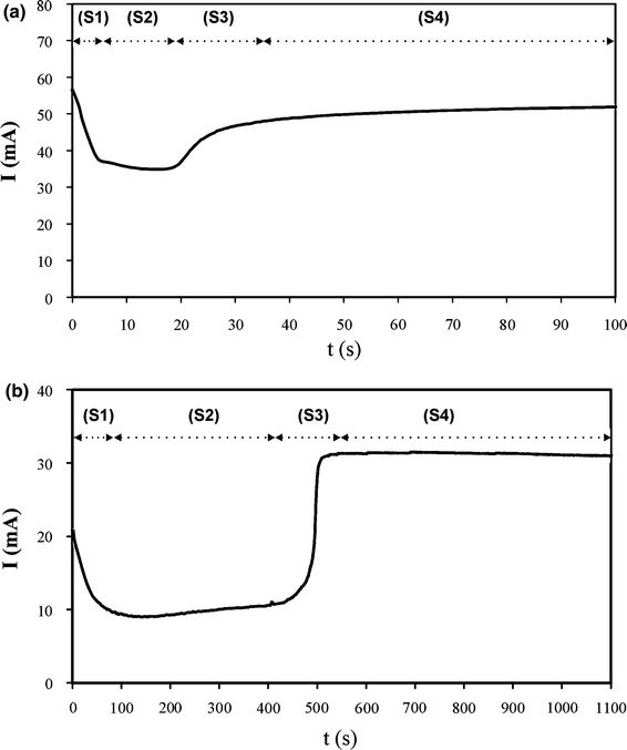
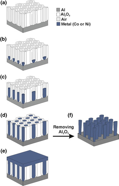
Figure 2 shows the typical current (I) versus time (t) characteristics, corresponding to the DC electrodeposition process of Co and Ni nanopillars. As we can see, there are four different sections in the current curve both for cobalt (Fig. 2a) and for nickel (Fig. 2b) electrodeposition, also observed in previous works [21,22]. In section 1 (S1), the current decreases abruptly until it reaches a steady value in section 2 (S2). Then, section 3 (S3) corresponds to a noticeable increase in the current curve until a second steady value is reached, corresponding to section 4 (S4). These four sections can be related to different stages of the growth of nanopillars in the pores. This process starts using as template an NAAM with opened pores at the aluminium–alumina interface (Fig. 3a). In the first section, metal nucleation centres in the pore bottom side start to grow (Fig. 3b). The decrease in the current can be explained by local depletion of the ionic concentration at the pore bottom [22]. The current stabilizes when the ionic diffusion can compensate for this depletion, and the metallic nanopillars grow filling the pores (section 2) (Fig. 3c). When the pores are entirely filled with Co and Ni, hemispherical tips of metal grow over the upper end of each nanopillar (Fig. 3d), resulting in the increase in current observed in S3. Finally (S4), a metallic film is formed on the NAAM surface (Fig. 3e). In order to obtain Co and Ni nanopillars without structural defects, the electrodeposition process must be finished at the end of the section 2 and the NAAM template must be removed (Fig. 3f).
Figure 2.

Typical current vs. time characteristic of the electrodeposition process.aFabrication of cobalt nanopillars process carried out at −3 V;bFabrication of nickel nanopillars process carried out at −5 V
Figure 3.

Slanted cross-section diagram describing the fabrication process of the metallic nanopillars.aNAAM template on aluminium substrate once the re-anodization process has finished;bA thin layer of metal is deposited at the pore bottom;cRapid growth of metallic nanopillars inside the NAAM template;dTotal filling with metal of the NAAM template pores;eMetal film formation on the NAAM surface;fResulting array of Co and Ni nanopillars when the process is stopped at the end of the section 2 (S2) [Fig. 2(a) and (b)] and the NAAM substrate is removed
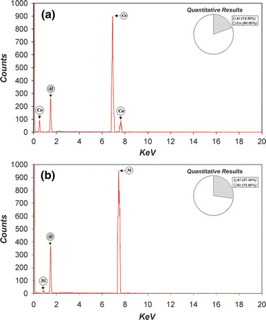
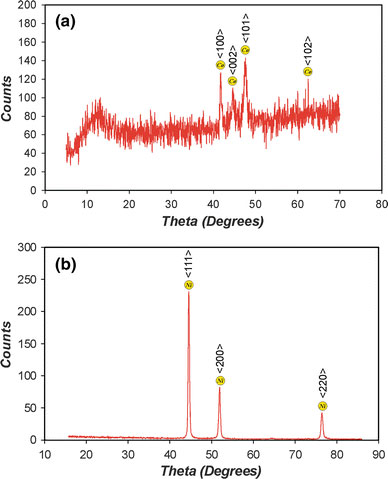
As was commented above, after electrodepositing Ni and Co NPs into the templates, the samples were post-treated in order to be characterized. First, the nanostructures were inspected by ESEM image analysis. Figure 4compiles a set of ESEM images of the Co NPs (Fig. 4a) and Ni NPs (Fig. 4b) in which it can be observed that these nanopillars remain fixed on the aluminium substrates (Fig. 4c, d). In addition, as Fig. 4e and f show, they keep the hexagonal arrangement corresponding to the NAAM used as template during the electrodeposition process. The average interpillar distance (about 250 nm) corresponds to the average interpore distance of the template, which means that the resulting nanostructure is tough enough to withstand the post-treatment. Moreover, the average pillar diameter (about 200 nm) is close to the average pore diameter of the template, and there are no structural defects in the resulting nanopillars. As we can see, it is confirmed that the average height of the nanopillars (around 12 μm) correspond to the thickness of the NAAM template. These facts imply that the electrodeposition process was carried out under suitable conditions, and the filling of the template pores was practically total. Secondly, in order to confirm the chemical elements, the nanostructures were analysed by EDXS. As Fig. 5shows, both the samples of Co (Fig. 5a) and Ni (Fig. 5b) nanopillars were exclusively composed of aluminium (corresponding to the Al substrate) and the respective metal (Co or Ni), what means that there was no chemical contamination post-treatment. The quantitative results were 19.5% Al and 80.5% Co for cobalt nanopillars and 27.3% Al and 72.7% Ni for nickel nanopillars. At last, the crystal phase of cobalt and nickel nanopillars was revealed by XRD analysis. As Fig. 6shows, both Co and Ni patterns of nanopillar arrays presented high-purity crystal phases since there were not any diffraction peaks of their corresponding oxides. The main peaks for Co nanopillars are four and appear at 41.6, 44.5, 47.4 and 62.5°, which correspond to 〈100〉, 〈002〉, 〈101〉 and 〈102〉 planes for a hexagonal crystal lattice, respectively (Fig. 6a). The main peaks for Ni nanopillars are three and appear at 41.5, 51.8 and 76.4°, which correspond to 〈111〉, 〈200〉 and 〈220〉 planes for a face-centred cubic crystal lattice, respectively (Fig. 6(b)).
Figure 4.

Set of ESEM images of the metallic nanopillars fabricated.aCross-section of an array of cobalt nanopillars on aluminium substrate after the removal of alumina template;bCross-section of an array of nickel nanopillars on aluminium substrate after the removal of the alumina template;cPore bottom detail on which we can see how the Co nanopillars are fixed on aluminium substrate;dPore bottom detail on which we can see how the Ni nanopillars are fixed on aluminium substrate;eTop view of an array of cobalt nanopillars;fTop view of an array of nickel nanopillars
Figure 5.

Elemental qualitative analysis of the samples by energy dispersive X-ray spectroscopy (EDXS).aSpectrum and weight percentage (inset) of the elements of the sample corresponding to Co nanopillars;bSpectrum and weight percentage (inset) of the elements of the sample corresponding to Ni nanopillars
Figure 6.

XRD patterns of cobalt (a) and nickel (b) nanopillar arrays
In summary, we have reported a simple and innovative electrochemical approach to fabricate cobalt and nickel nanopillar arrays on aluminium substrates. This technique improves other methods previously proposed, because the number of stages in the fabrication process is smaller. For this reason, it is faster and more cost-effective than previous works. This advantage is due mainly to the fact that the removal of aluminium oxide from the pore bottom tips in the NAAM template takes place in the same electrolyte in which the anodization is carried out. Another main feature of this process is that the Co and Ni nanopillars remain on the aluminium substrate after removing the NAAM template. In addition, the technique presented here can be applied to NAAMs produced by both the MA and HA techniques with different acids, which opens a wide range of nanopillar morphologies. The nanopillar diameter and weight and the interpillar distance can be established beforehand by modifying the anodization parameters (anodization voltage, acid and concentration mainly).
By applying this technique with other methods for fabricating this kind of nanostructures, it is expected that the present method can be used to produce novel nanostructures such as nanotube arrays. This is a promising technique for future applications and a means for fabricating new nanodevices. One example of a future application of the resulting structure presented in this work could be using the metallic nanopillars as nanoelectrodes for the direct deposition of nanoparticles from a gas draught. This nanostructure would act as an electrostatic precipitator by applying a high-voltage field.
Acknowledgments
This work was supported by the Spanish Ministry of Education and Science (MEC) under grant number TEC2006-06531 and CONSOLIDER HOPE project CSD2007-00007.
References
- Al Mawlawi D, Coombs N, Moskovits M. J. 1991. p. 4421. COI number [1:CAS:528:DyaK3MXmsVKgsrc%3D]; Bibcode number [1991JAP....70.4421A] [DOI]
- Kruis FE, Nielsch K, Fissan H, Rellinghaus B, Wasserman EF. Appl. 1998. p. 547. COI number [1:CAS:528:DyaK1cXksleitL0%3D]; Bibcode number [1998ApPhL..73..547K] [DOI]
- Gorokh G, Mozalev A, Solovei D, Khatko V, Llobet E, Correig X. Electrochim. Acta. 2006. p. 1771. COI number [1:CAS:528:DC%2BD28Xht1emt77P] [DOI]
- Wang J, Myung NV, Yun M, Monbouquette HG. J. 2005. p. 139. COI number [1:CAS:528:DC%2BD2cXhtFejs7jK] [DOI]
- Jessensky O, Müller F, Gösele U. Appl. 1998. p. 1173. COI number [1:CAS:528:DyaK1cXhsVyrsL8%3D]; Bibcode number [1998ApPhL..72.1173J] [DOI]
- Masuda H, Yamada H, Satoh M, Asoh H, Nakao M, Tamamura T. Appl. 1997. p. 2770. COI number [1:CAS:528:DyaK2sXntFCrurs%3D]; Bibcode number [1997ApPhL..71.2770M] [DOI]
- Masuda H, Fukuda K. Science. 1995. p. 1466. COI number [1:CAS:528:DyaK2MXmtFKktbc%3D]; Bibcode number [1995Sci...268.1466M] [DOI] [PubMed]
- Routkevitch D, Tager AA, Haruyama J, Almawlawi D, Moskovits M, Xu JM. IEEE Trans. 1996. p. 1646. Bibcode number [1996ITED...43.1646R] [DOI]
- Wang Z, Brust M. Nanoscale Res. 2007. p. 34. COI number [1:CAS:528:DC%2BD2sXhsVSgtLk%3D]; Bibcode number [2007NRL.....2...34W] [DOI]
- Inguanta R, Butera M, Sunseri C, Piazza S. Appl. 2007. p. 5447. COI number [1:CAS:528:DC%2BD2sXislSqs7c%3D]; Bibcode number [2007ApSS..253.5447I] [DOI]
- Lakshmi BB, Dorhout PK, Martin CR. Chem. 1997. p. 857. COI number [1:CAS:528:DyaK2sXhtlCru7k%3D] [DOI]
- Fan Z, Dutta D, Chien CJ, Chen HY, Brown EC, Chang PC, Lu JG. Appl. 2006. pp. 213110–213111. Bibcode number [2006ApPhL..89u3110F] [DOI]
- Wang Q, Sun X, Luo S, Sun L, Wu X, Cao M, Hu C. Cryst. 2007. p. 2665. COI number [1:CAS:528:DC%2BD2sXht1Gmt77J] [DOI]
- Zhang XY, Zhang LD, Chen W, Meng GW, Zheng MJ, Zhao LX. Chem. 2001. p. 2511. COI number [1:CAS:528:DC%2BD3MXltlCmu74%3D] [DOI]
- Sui YC, Cui BL, Martínez L, Pérez R, Sellmyer DJ. Thin Solid Films. 2002. p. 64. COI number [1:CAS:528:DC%2BD38Xjt1Kju7o%3D]; Bibcode number [2002TSF...406...64S] [DOI]
- Nielsch K, Müller F, Li A, Gösele U. Adv. 2000. p. 582. COI number [1:CAS:528:DC%2BD3cXkslCjurc%3D] [DOI]
- Kazadi A, Rivas J, Zaragoza G, López-Quintela MA, Blanco MC. J. 2001. p. 3393. Bibcode number [2001JAP....89.3393K] [DOI]
- A. Santos, L. Vojkuvka, J. Pallare´s, J. Ferre´-Borrull, L.F. Marsal (2009) J. Electroanal. Chem. (accepted). doi: 10.1016/j.jelechem.2009.04.008.
- Lee W, Ji R, Gösele U, Nielsch K. Nat. 2006. p. 741. COI number [1:CAS:528:DC%2BD28XovFyks74%3D]; Bibcode number [2006NatMa...5..741L] [DOI] [PubMed]
- Vojkuvka L, Marsal LF, Ferré-Borrull J, Formentin P, Pallarés J. Superlattices Microstruct. 2008. p. 577. COI number [1:CAS:528:DC%2BD1cXht1KmsrvO]; Bibcode number [2008SuMi...44..577V] [DOI]
- Whitney TM, Jiang JS, Searson PC, Chien CL. Science. 1993. p. 1316. COI number [1:CAS:528:DyaK3sXmtFGqsL4%3D]; Bibcode number [1993Sci...261.1316W] [DOI] [PubMed]
- Shönenberger C, van der Zande BMI, Fokkink LG, Henny M, Schmid C, Krüger M, Bachtold A, Huber R, Birk H, Staufer U. J. Phys. Chem. B. 1997. p. 5497. [DOI]


