Abstract
The field emission properties of SnO2nanowires fabricated by chemical vapor deposition with metallic catalyst-assistance were investigated. For the as-fabricated SnO2nanowires, the turn-on and threshold field were 4.03 and 5.4 V/μm, respectively. Considerable enhancement of field emission of SnO2nanowires was obtained by a post-annealing process in oxygen at high temperature. When the SnO2nanowires were post-annealed at 1,000 °C in oxygen, the turn-on and threshold field were decreased to 3.77 and 4.4 V/μm, respectively, and the current density was increased to 6.58 from 0.3 mA/cm2at the same applied electric field of 5.0 V/μm.
Keywords: SnO2nanowires, Chemical vapor deposition, Field emission, Annealing
Introduction
SnO2 is an important n type wide-band gap (E.g. = 3.6 eV, at 300 K) semiconducting material, which exhibits extensive applications in the fields of gas sensors, transparent conducting electrodes, transistors, electrode materials, catalysis, solar cells, and optoelectronic devices [1-5]. Recently, various SnO2 nanostructures [6-9] have been proved to be promising candidates for field emission-based flat panel displays due to their characteristic properties of high physical and chemical stability and causticity resistance, compared with ZnO nanostructures and carbon nanotubes. These excellent demonstrations of electron emission from SnO2 nanostructures have opened the door to a new area of applications of these materials for the production of efficient cold cathodes. In order to develop efficient and controllable field emission devices based on SnO2 nanostructures at a lowest energy expense, effective methods to optimize their field emission properties are highly desirable to achieve the highest current density at the lowest threshold electric field. However, the researches specialized on how to enhance the field emission properties of SnO2 nanostructures have been limited to only a few reports [10,11]. In this paper, SnO2 nanowires are fabricated by a chemical vapor deposition method with metallic catalyst-assistance. It is found that the post-annealing process in oxygen is an effective method for enhancing the field emission of SnO2 nanowires.
Experimental Method
A chemical vapor deposition method with metallic catalyst-assistance was employed for the preparation of SnO2 nanowires [7,10]. A layer of Au (about 7 nm in the thickness) as a catalyst was first deposited on Si substrates with the area of ~8 mm2 by DC sputtering. Commercial SnO2 powders (99.9%) and graphite powders (99.99%) were mixed in a 3:1 molar ratio, transferred to a carnelian mortar and skived for 30 min to make the starting materials well mixed. The mixture was placed into a small quartz tube, and then the substrate was put near the mixture at a distance about 1.5 cm. The small quartz tube was pulled into the center of the large quartz tube furnace. During the whole reaction process, Ar (99.999%) was used as a carrier gas to create the inert atmosphere inside the furnace. When the tube furnace was pumped to 8 Torr by a mechanical pump, the starting materials were heated to 950 °C from room temperature in 30 min and kept at 950 °C for 15 min. After this process, the furnace was cooled down to room temperature in several hours. Finally, the substrate with a gray film-like production was taken out from the small quartz tube and used for analysis. The as-grown SnO2 nanowires were post-annealed in oxygen for 1 h at 700, 850, 900, 950, and 1,000 °C, respectively.
The general morphologies of the as-fabricated SnO2nanowires were characterized by a scanning electron microscope (SEM, LEO-1525). Phase identification and degree of crystallinity of the samples were studied by a D/max -rA X-ray diffractometer with Cu–Kα radiation using normal θ–2θ scanning method. The microstructure and composition of the samples were studied with a JEOL JEM-2100 transmission electron microscope (TEM), a high resolution-transmission electron microscope (HR-TEM) and an energy-dispersive X-ray spectroscope (EDX) attached to the TEM instrument. Field emission measurements for SnO2nanowires were carried out with diode structure in a vacuum chamber at a pressure of 5 × 10⁻⁶ Torr at room temperature. The sample (as a cathode) was separated from a Cu probe anode. The voltage with an increasing step was continuously applied from a Cu probe (anode) to the sample (cathode) until a short-current was detected.
Results and Discussion
Structural Analyses
The crystal structure of the as-grown SnO2samples was detected by XRD. Figure 1a shows XRD patterns of (a) as-grown and post-annealed SnO2nanowires at (b) 700 °C, (c) 850 °C and (d) 1,000 °C, respectively. All the diffraction peaks in the pattern can be indexed as a crystal structure of the tetragonal rutile SnO2structure with lattice constants ofa = 0.474 nm andc = 0.318 nm, consistent with the standard data file (ICDD-PDF41-1445). It can be seen from Fig. 1a that the intensity of the (101) peak is much higher than those of the other peaks, indicating a growth preference in the (101) direction for the SnO2nanowires. Figure 1b shows the (101) diffraction peaks of the as-grown and all the post-annealed SnO2nanowires, and the inset shows the values of the full width at half maximum (FWHM) and the intensity of the (101) peaks as a function of annealing temperature. One can see that with increasing annealing temperature, the intensity of the (101) peaks increases, while FWHM decreases gradually, which indicates that the crystallization of the nanowires is gradually improved by a post-annealing procedure in oxygen.
Figure 1.
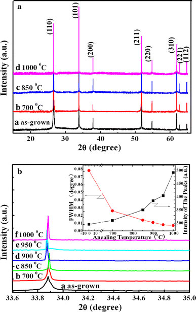
aXRD patterns ofaas-grown and post-annealed SnO2nanowires atb700 °C,c850 °C, andd1,000 °C, respectively.bThe (101) diffraction peak ofaas-grown and post-annealed atb700 °C,c850 °C,d900 °C,e950 °C andfannealed at 1,000 °C, respectively, inset is the variation of the FWHM and the intensity of the peaks as a function of annealing temperature
Scanning electron microscope (SEM) morphologies of the fabricated nanowires are shown in Fig. 2. As shown in Fig. 2, the as-fabricated nanowires are homogeneous compact tangly and randomly extending. The length of the nanowires is more than 10 μm and the width is in the range of 30–95 nm. Note that we estimate the length of the synthesized nanowires by some low magnification SEM images in this study. For example, in Fig. 2, we use the scale bar to measure the length, in which we can easily find many nanowires with size more than 10 μm.
Figure 2.
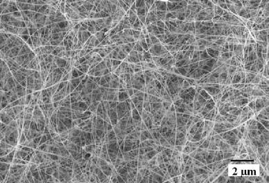
SEM image of as-fabricated nanowires
The morphology and microstructure of the as-fabricated SnO2 nanowires was performed by TEM. Figure 3a exhibits the TEM image of as-grown SnO2 nanowires. The HR-TEM image of the selected region in (a) is shown in Fig. 3b, which indicates that the entire nanowire is a single crystal. The image of Fig. 3b shows a perfect lattice of the SnO2 rutile structure and the measured lattice spacing is approximately 0.26 nm ascribed to the (101) plane. It is deemed that the growth preference direction of SnO2 nanowires is the (101) direction, consistent with the XRD pattern. Energy dispersive X-ray spectroscopy (EDS) analysis is presented in Fig. 3c, which reveals the presence of Sn and O, indicating the formation of SnO2. Some unmarked signals in the EDS spectrum come from the TEM grid used. It should be noted that the EDS data show the ratio of O to Sn is 1.51 for the as-grown nanowires, which is much lower than the stoichiometric ratio of SnO2. But it is confirmed by both the XRD and HR-TEM image analysis that the as-grown nanowires are SnO2 not Sn2O3. It is common that there are many oxygen vacancies in SnO2 nanowires due to the lack of oxygen during the growth of nanostructures by this chemical vapor deposition method [7,11]. Figure 3d shows that the atomic ratio of O to Sn in SnO2 nanowires increases gradually with the increment of annealing temperature. It indicates that the oxygen vacancies in the as-grown SnO2 nanowires are compensated by post-annealing in oxygen.
Figure 3.
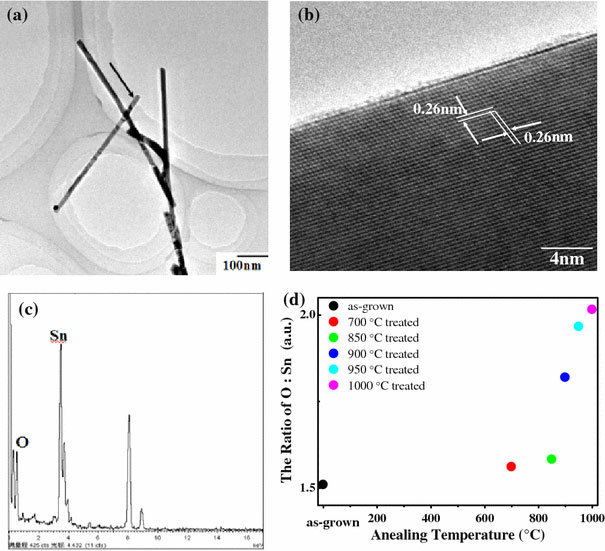
aTEM images of SnO2nanowires,bHRTEM images of SnO2nanowires,cthe EDS spectrum of SnO2nanowires,dthe ratio of O to Sn in SnO2nanowires annealed at different temperatures
Field Emission Performance
Figure 4 shows the relation of field emission current density (J) and the applied electric field (E) measured at an anode–cathode separation of about 160 μm for the as-fabricated SnO2 nanowires. Generally speaking, the turn-on field is defined as the applied electric field where current density is distinguished from the background noise, and the threshold field is defined as the E where the J arrives at 1 mA/cm2[12]. From the J-E curve, the turn-on and threshold fields are about 4.03 and 5.4 V/μm, respectively. And the field emission current density is approximately 0.3 mA/cm2 at the applied electric field of 5.0 V/μm.
Figure 4.
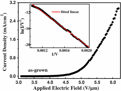
Field-emissionJ-Ecurve for the as-grown SnO2nanowires. Inset is the corresponding F–N plot
The inset of Fig. 4 is the corresponding Fowler–Nordheim (F–N) plot. The plot goes near to a straight line, which indicates that the field emission from SnO2 nanowires follows the F–N relationship and reveals that the field emission process is a barrier tunneling quantum mechanical process [13-15].
Usually, the classic F–N law [16] is used to describe the relationship between the field-emission-current density J and the local electric field Eloc to give a profound analysis of the emission properties. The F–N equation can be depicted as:
| (1) |
where J is the field-emission-current density, Φ is the barrier height for the emission surface (the work function for SnO2 is 4.5 eV [17]). a and b are constants with the value of 1.54 × 10⁻¹⁰ (A V−2 eV) and 6.83 × 10³ (V eV−3/2 μm−1), respectively. Eloc represents the applied local electric field around the probe. Eloc could be up to hundreds or thousands times of the macroscopic electric field between the anode and the cathode. Eloc can be described as:
| (2) |
where V is the applied voltage, d is the distance between the anode and the cathode. β is the field enhancement factor, which reflects the ability of the emitters to enhance the applied local electric field around the probe compared to the macroscopic electric field. The value of β is related to the emitter geometry morphology, the crystal structure, and the spatial distribution of emitting centers.
From the Eqs. (1) and (2), the F–N equation could be predigested as:
| (3) |
whereIis the field emission current. And then, the field enhancement factorβcan be estimated by dint of the slopesSof the fitted straight lines of the F–N plots, viz.  . Consequently, the field enhancement factorβof the as-fabricated SnO2nanowires is 1,008.
Figure 5shows the field emission properties of SnO2nanowires post-annealed in oxygen at different temperatures. These curves indicate the functions between field-emission-current density and applied electric field. One can see that excellent field emission properties of the post-annealed SnO2nanowires are achieved. Compared with the as-fabricated SnO2nanowires, the turn-on and threshold fields are decreased, and the current density is increased. When the annealing temperature is higher than 700 °C, the field emission current density increased hastily with the increment of the annealing temperature. After annealing at 1,000 °C, the turn-on and threshold fields of SnO2nanowires are decreased to 3.77 and 4.4 V/μm, respectively. It is noteworthy that the current density is up to 6.58 mA/cm2at the applied electric field of 5.0 V/μm, which is almost 22 times of that of as-fabricated SnO2nanowires. Hereby, post-annealing process in oxygen at high temperature is an effective method to considerably improve the field emission properties of SnO2nanowires.
Figure 5.
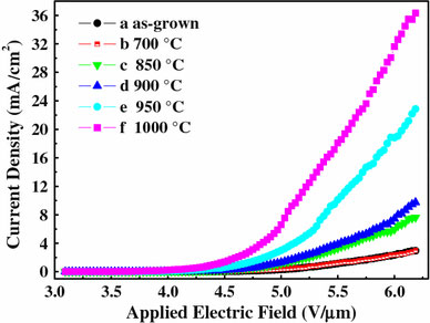
Field-emissionJ-Ecurves foraas-grown and post-annealed SnO2nanowires in oxygen atb700 °C,c850 °C,d900 °C,e950 °C andf1,000 °C, respectively
Discussion
In general, the field emission properties depend on the field enhancement factor β and the work function of the sample. The field enhancement factor depends on both the tip morphology and the density of the nanostructures. Usually, nano-structured SnO2 with a high aspect ratio show good field emission performance, due to their much higher β value. Therefore, the shorter and thinner nanowires may be propitious to FE process and beneficial to improve the FE properties. Additionally, in the SnO2 nanostructures case, the catalysts such as Au nanoparticles seem no significant influence of the FE performance of SnO2 nanostructures [6,7,10,18]. Table 1 summarized the FE properties of different SnO2 nanostructures, such as hierarchical sallowlike [9], fishbone-like nanostructures [9], nanowhiskers [10], beaklike nanorods [18], and zigzag nanobelts [19]. From Table 1, one can see that FE properties of SnO2 can be enhanced by optimizing the morphologies of SnO2 nanostructures, but the FE current of SnO2 nanostructures is lower than 1 mA/cm2 (at 5 V/μm). Recently, Jang et al.[11] have found that the FE properties of SnO2 nanowires can be improved by a post-treatment of H2 exposure process. But the H2 exposure treatment cannot effectively compensate oxygen vacancies generated during the growth process. Figures 1 and 3 clearly show that oxygen vacancies are effectively compensated and the perfect of crystal is improved, so the FE properties of SnO2 nanowires annealed at high temperature in oxygen can be improved.
Table 1.
FE properties of different morphologies of SnO2nanostructures
| Different morphologies | Turn-on field (Vμm−1) | Threshold field (Vμm−1) | Current density (at 5 Vμm−1) mA/cm2 | References |
|---|---|---|---|---|
| Sallow-like |
1.88 |
3.98 |
– |
[9] |
| Fishbone-like |
2.36 |
2.87 |
~1.0 |
[9] |
| Beaklike nanorods |
5.8 |
– |
– |
[18] |
| Nanowhiskers |
1.37 |
– |
~0.1 |
[10] |
| Zigzag nanobelts |
1.9 |
5.1 |
~0.9 |
[19] |
| As-grown nanowires |
4.03 |
5.4 |
0.3 |
This paper |
| Nanowires post-annealed in O2at 1,000 °C | 3.77 | 4.4 | 6.58 | This paper |
The main reason for the low the turn-on and threshold fields, large current density of high temperature treated SnO2nanowires in oxygen can be probably attributed to the following factors: the high crystalline structure and the reduction of the oxygen vacancy concentration. Generally, the high temperature annealing can greatly improve the perfect of crystal, which can be seen from Fig. 1. Thus the improvement of crystalline structure of the treated nanowires is benefit to the field emission performance of nanowires. For nanostructures of semiconductor, it is well known that surface states play an important role in influencing the carrier concentration, carrier mobility, and the effective barrier height. Therefore, these surface states can act as electron traps, forming a high potential barrier on the nanowires surface to reduce the conductivity. Thermal annealing with high temperature in oxygen could not only promote the crystalline quality of nanostructures by removing structural defects such as point defects, but also passivate the surface defects such as oxygen vacancies of SnO2nanowires. Importantly, our XRD data show that the crystalline quality of SnO2nanowires is highly promoted by high temperature annealing in Fig. 1. Meanwhile, our EDS spectrums clearly show that the increase of O atomic content with the annealing temperature increased in Fig. 3.
On the other hand, the reduction of the oxygen vacancy concentration of SnO2nanowires can decrease the surface barrier. Then, the Fermi level heightens and moves to the bottom of conduction band, and the carrier concentration and conductivity increase. Therefore, the work function becomes smaller and field emission property is enhanced. To quantificationally understand the influence of the annealing temperature on the work functions, the F–N plots are conducted as shown in Fig. 6. Here, the field emission factorβis considered to be the same before and after treatments, because the morphology and surface density of the nanowires are not changed very much after treatments. According to the F–N plots, the work functions are estimated in virtue of the slopesSand the field emission factorsβ. Figure 7shows the work function of SnO2nanowires as a function of annealing temperature. As shown in Fig. 7, the work function decreases exponentially with increasing the annealing temperature. Accordingly, the corresponding current density at 6 V/μm increases exponentially with the increment of annealing temperature, which is also shown in Fig. 7.
Figure 6.
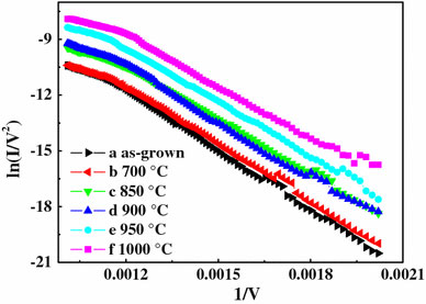
F–N plots foraas-grown and post-annealed SnO2nanowires in oxygen atb700 °C,c850 °C,d900 °C,e950 °C andf1,000 °C, respectively
Figure 7.
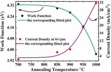
The work function and corresponding current density at 6 V/μm as a function of the annealing temperature
Conclusions
In conclusion, the homogeneous compact tangly SnO2nanowires were synthesised by chemical vapor deposition with metallic catalyst-assistance. The considerable enhancement of field emission from SnO2nanowires is observed by post-annealing the nanowires in oxygen at high temperatures. The turn-on and threshold fields of SnO2nanowires decreases and the current density increases with the increment of annealing temperature. The enhancement of field emission from SnO2nanowires is considered to be related with the reduction of the oxygen vacancy concentration in nanowires by post-annealing in oxygen at high temperature.
Acknowledgments
This work was financially supported by the National Natural Science Foundation of China (Nos. 50702048 and 10525211), the Project supported by Hunan Provincial Natural Science Foundation of China (Nos. 09JJ1006), and the Specialized Research Fund for the Doctoral Program of Higher Education (No. 20070530010).
References
- Hollamby PC, Aldridge PS, Moreti G, Egdell RG. Surf. 1993. p. 393. COI number [1:CAS:528:DyaK3sXovF2gtg%3D%3D]; Bibcode number [1993SurSc.280..393H] [DOI]
- Varghese OK, Malhotra LK. Sens. Actuat. B. 1998. p. 19. [DOI]
- Baughman RH, Zakhidov AV, DeHeer WA. Science. 2002. p. 787. COI number [1:CAS:528:DC%2BD38XlvVyhsrw%3D]; Bibcode number [2002Sci...297..787B] [DOI] [PubMed]
- Senda S, Sakai Y, Mizuta Y, Kita S, Okuyama F. Appl. 2004. p. 5679. COI number [1:CAS:528:DC%2BD2cXhtVKqsLnL]; Bibcode number [2004ApPhL..85.5679S] [DOI]
- Huang XMH, Zorman CA, Mehregany M, Roukes ML. Nature. 2003. p. 496. COI number [1:CAS:528:DC%2BD3sXntFSkug%3D%3D]; Bibcode number [2003Natur.421..496H] [DOI] [PubMed]
- Chen YJ, Li QH, Liang YX, Wang TH. Appl. 2004. p. 5682. COI number [1:CAS:528:DC%2BD2cXhtVKqsLnF]; Bibcode number [2004ApPhL..85.5682C] [DOI]
- Wang B, Yang YH, Wang CX, Xu NS, Yang GW. J. 2005. p. 124303. Bibcode number [2005JAP....98l4303W] [DOI]
- Deshpande AC, Koinkar PM, Ashtaputre SS, More MA, Gosavi SW, Godbole PD, Joag DS, Kulkarni SK. Thin. 2006. p. 1450. COI number [1:CAS:528:DC%2BD28Xht1WrurbM]; Bibcode number [2006TSF...515.1450D] [DOI]
- Wang QY, Yu K, Xu F. Solid. 2007. p. 260. COI number [1:CAS:528:DC%2BD2sXntFeitb0%3D]; Bibcode number [2007SSCom.143..260W] [DOI]
- Luo SH, Wan Q, Liu WL, Zhang M, Dai ZF, Wang SY, Song ZT, Lin CL. Nanotechnology. 2004. p. 1424. COI number [1:CAS:528:DC%2BD2MXhsV2gsg%3D%3D]; Bibcode number [2004Nanot..15.1424L] [DOI]
- Jang HS, Kang SO, Kim YI. Solid. 2006. p. 495. COI number [1:CAS:528:DC%2BD28XhtF2js7vO]; Bibcode number [2006SSCom.140..495J] [DOI]
- Li MK, Wang DZ, Ding YW, Guo XY, Ding S, Jin H. Mater. Sci. Eng. A. 2007. p. 417. [DOI]
- Rinzler AG, Hafner JH, Nikolaev P, Lou L, Kim SG, Tomnek D, Nordlander P, Colbert DT, Ugarte D. Science. 1995. p. 1550. COI number [1:CAS:528:DyaK2MXotVOgsbo%3D]; Bibcode number [1995Sci...269.1550R] [DOI] [PubMed]
- DeHeer WA, Chatelain A, Ugarte D. Science. 1995. p. 1179. COI number [1:CAS:528:DyaK2MXpsVyktL8%3D]; Bibcode number [1995Sci...270.1179D] [DOI] [PubMed]
- Au FCK, Wang KW, Tang YH, Zhang YF, Bello I, Lee ST. Appl. 1999. p. 1700. COI number [1:CAS:528:DyaK1MXlslKgtLw%3D]; Bibcode number [1999ApPhL..75.1700A] [DOI]
- Fowler RH, Nordheim LW. Proc. R. Soc. London, Ser. A. 1928. p. 172. Bibcode number [1928RSPSA.119..173F]
- Szuber J, Czempik G, Larciprete R, Adamowicz B. Sens. Actuat. B. 2000. p. 177. [DOI]
- He JH, Wu TH, Hsin CL, Li KM, Chen LJ, Chueh YL, Chou LJ, Wang ZL. Small. 2006. p. 116. COI number [1:CAS:528:DC%2BD2MXhtlWqsrjK] [DOI] [PubMed]
- Wu J, Yu K, Li LJ, Xu JW, Shang DJ, Xu YE, Zhu ZQ. J. 2008. p. 185302.


