Abstract
Zinc oxide nanowires have been synthesized without using metal catalyst seed layers on fluorine-doped tin oxide (FTO) substrates by a modified vapor phase transport deposition process using a double-tube reactor. The unique reactor configuration creates a Zn-rich vapor environment that facilitates formation and growth of zinc oxide nanoparticles and wires (20–80 nm in diameter, up to 6 μm in length, density <40 nm apart) at substrate temperatures down to 300°C. Electron microscopy and other characterization techniques show nanowires with distinct morphologies when grown under different conditions. The effect of reaction parameters including reaction time, temperature, and carrier gas flow rate on the size, morphology, crystalline structure, and density of ZnO nanowires has been investigated. The nanowires grown by this method have a diameter, length, and density appropriate for use in fabricating hybrid polymer/metal oxide nanostructure solar cells. For example, it is preferable to have nanowires no more than 40 nm apart to minimize exciton recombination in polymer solar cells.
Keywords: Zinc oxide, Semiconducting II–VI materials, Nanowires, Chemical vapor deposition, Low temperature, Transparent oxide
Introduction
Zinc oxide (ZnO) is a wide bandgap (3.4 eV) II–VI compound semiconductor that has recently garnered great interest due to its unique properties and potential applications in fabricating high performance and high efficiency electronic [1], optoelectronic [2], photovoltaic [3], as well as electrochemical and electromechanical devices of nanoscale dimensions [4]. In particular, ZnO nanowires have shown promise to enhance the power conversion efficiency of conjugated polymer-based solar cells [5,6], which are viable candidates to address the global need for inexpensive alternative energy sources. The function of the nanowire is to increase electron mobility and reduce the electron recombination rate within the conjugated polymer. These functions are accomplished by the nanowire providing a heterojunction interface that dissociates photogenerated excitons into electrons and holes. Due to its high-energy electronic band structure, the nanowire provides a direct conduit for electrons to be transported to the device electrode where it can contribute to current conduction. If the nanowires are closely spaced, approximately twice the exciton diffusion length (<40 nm) where recombination occurs, then the rate of recombination is minimized thus enhancing power conversion efficiency [7]. To date, power conversion efficiencies up to ~2% have been reported for hybrid ZnO nanowire/polymer solar cells [5,6].
In order to fabricate hybrid nanowire solar cells, the nanowire must be electrically connected to the device electrode. Typically, the device electrode is made of a transparent conductive oxide such as fluorine-doped tin oxide (FTO) or indium tin oxide (ITO) deposited on glass. Thus, it is desirable to synthesize nanowires directly on the electrode. Many studies have reported direct synthesis of ZnO nanowires on ITO and FTO via solution-based chemical methods [8,9]. Very few physical synthesis methods exist that are compatible with transparent oxide substrates due to the high synthesis temperatures that are 900–1,200°C [10]. High temperatures have been shown to degrade the oxide conductivity [11].
Physical synthesis methods, such as chemical vapor deposition (CVD) and vapor phase transport (VPT) [10], offer a number of advantages when compared to chemical methods. First, many of these methods do not require catalyst or seed layers as nanowires can be grown directly from the substrate. Second, because the nanostructure of the ZnO is determined mainly by the local temperature and reaction time, these parameters can be adjusted to control the product morphology and size. Third, the synthesis of nanowires by solution-based chemistry usually involves environmentally unfriendly organic solvents and takes from 2 to 12 h while it takes less than 2 h via physical synthesis. Thus, physical synthesis methods are more efficient in producing high-quality ZnO nanowires. There is a need to explore new low temperature physical synthesis methods since transparent oxide substrates and emerging polymer-based flexible electronics require processing temperatures less than 500°C to prevent substrate or existing device layer damage.
Recently, ZnO nanowires and nanorods were synthesized via VPT on silicon at 500°C using zinc chloride as the source material [12]. Another study reported synthesis of ZnO nanotips on FTO at 470°C by metal organic chemical vapor deposition (MOCVD) [13]. In this study, we put our work into context by reporting the direct physical synthesis of ZnO nanowires on an FTO substrate via a new VPT process that utilizes a miniature reaction tube at substrate temperatures down to 300°C. A parametric study of the effects of furnace temperature, reaction time, and carrier gas flow rate on the length, diameter, and number density of ZnO nanowires has been conducted. The goal of these experiments is to determine an optimized combination of these three controllable parameters to produce ZnO nanowires with the desired morphology.
Experiment
ZnO nanowires were synthesized using a CVD system as illustrated in Fig. 1. It consists of a tube furnace integrated with a thermocouple at the center of the furnace, a 50-mm quartz reaction tube, a mass flow rate controller, and a vacuum pump. A 23 cm long by 10 mm diameter miniature quartz tube was placed inside the larger 50-mm tube with its closed-end pointing toward the gas inlet side of the larger tube. This “double-tube” system configuration is similar to previous studies [14,15]; however, it is different in that the present configuration allows for synthesis at substrate temperatures down to ~300°C while utilizing no metal catalyst (such as Au). In this unique configuration, the miniature reaction tube confines the vapor to maintain a high zinc concentration environment inside the quartz tube.
Figure 1.
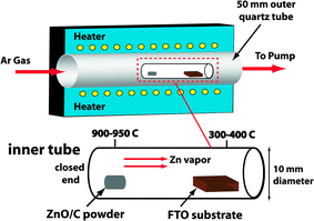
Diagram of CVD system with double-tube configuration. A 10-mm diameter miniature quartz reactor tube is housed inside of a 50-mm reactor tube. The miniature tube confines the Zn vapor to create a high Zn concentration environment
The precursor material consisted of a mixture of high-quality ZnO (99.999%, Sigma-Aldrich) and C (graphite, 99.999%, Sigma–Aldrich) powders in a 1:1 ZnO/C ratio by weight. Approximately 60 mg of the mixture was used per experimental run. The precursor was placed at the closed-end of the miniature tube, which was located in the high-temperature zone (900–1,000°C) of the furnace. The substrate was located ~12–15 cm downstream of the precursor toward the open-end of the tube in the low-temperature zone (300–400°C). Temperature zones inside the tube furnace were identified by temperature-profiling experiments. Hereafter, note that the growth temperature refers to the temperature at the precursor (high-temperature zone). Temperatures were measured at 0.5-cm intervals along the quartz tube inside the furnace using a thermocouple.
Synthesis was performed on 0.5 square cm FTO-coated glass substrates (Hartford Glass, Hartford, IN, USA; 12.5–14.5 Ω per square; 400 nm oxide thickness). The substrates were cleaned prior to synthesis by the following sequence: sonication in (a) acetone, (b) propanol, and (c) ethanol. Then, substrates were rinsed in deionized water and dried via nitrogen gas.
The synthesis procedure consisted of the following steps. First, upon proper placement of the precursor and substrate in the tube furnace, the temperature of the furnace was ramped from room temperature (~22°C) to the growth temperature of 900–1,000°C at 760 Torr over 15 min with a constant flow (70–200 sccm) of Ar (carrier gas). Next, the specific growth temperature was maintained for reaction times varying from 30 to 120 min. Finally, the furnace was cooled down to room temperature, and the substrates were extracted from the tube furnace. The growth temperature, reaction time, and Ar flow rate were independently varied to study the effect of growth parameters on product formation.
The synthesized product size, morphology, and distribution as a function of reaction time, growth temperature, and Ar flow rate were characterized using scanning electron microscopy (SEM) (Zeiss EVO MA 15). Energy dispersive X-ray spectroscopy (EDX) attached to the SEM was used to characterize the chemical composition of the products. The crystalline structure was investigated by X-ray diffraction in a Panalytical X’Pert MRD instrument using Cu Kα radiation and a parallel beam geometry.
Results
Effect of Reaction Time
The first group of experiments was carried out at 950°C under an Ar flow rate of 70 sccm. The reaction times were 30, 80, 100, and 120 min. Figure 2 shows the SEM images taken from these experiments, which revealed the effect of growth time on the average diameter and length of as-synthesized ZnO nanowires.
Figure 2.
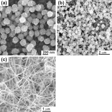
SEM images of ZnO nanostructures synthesized on FTO-coated glass substrates after a 30, b 80, and c 100 min at the furnace temperature of 950°C, 760 Torr, and Ar flow rate of 70 sccm
After 30 min, dispersively distributed faceted nanoparticles with diameters ranging from 100 to 250 nm were formed on the substrates (Fig. 2a). The faceted morphology and EDX analysis (not shown here) of multiple samples indicate the formation of ZnO nanoparticles. Additionally, it can be seen that the nanoparticles stack upon one another indicating that they do not nucleate from surface droplets or a film layer. As the reaction time increases, these nanoparticles served as seed layers for the growth of ZnO nanowires. When the growth time reached 80 min, ZnO nanowires were observed to form. Figure 2b shows the morphology, size, and number density of the wires. The nanowires have dimensions of 30–40 nm in diameter and 1–2 μm in length. Thus, Fig. 2a, 2b show that the evaporated Zn generates a highly saturated vapor that forms ZnO nanoparticles, which then catalyze the growth of ZnO nanowires.
With increasing growth time, the nanowires continue to grow longer. The ZnO nanowires synthesized at 100 min have an average diameter of 40–60 nm and length up to 4 μm (Fig. 2c). Compared to those grown for a shorter time, the average diameter did not change significantly, indicating the growth time had a greater effect on the length than the diameter of the nanowire. The nanowires appear to grow straight and have a narrow size distribution. The nanowires do not appear to be vertically aligned, which is expected since epitaxial growth with the substrate does not occur and growth is from the particles. The dependence of the nanowires’ average length and diameter on the reaction time is shown in Fig. 3. After nanoparticle formation, the length follows an approximately linear relationship with time. This is indicative that growth is limited by the supply of Zn from the vapor phase.
Figure 3.
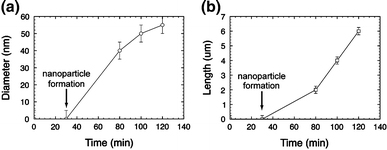
ZnO nanowire diameter and length as a function of reaction time at 950°C, 760 Torr, and Ar flow rate of 70 sccm
Effect of Reaction Temperature
The effects of growth temperature on the size, morphology, and number density of synthesized ZnO nanowires have also been investigated. The second group of experiments was conducted under fixed conditions of 70 sccm Ar flow rate, 760 Torr, and 100-min reaction time. ZnO nanowires were synthesized at growth temperatures of 910, 930, 940, 950, and 1,000°C as shown in Fig. 4.
Figure 4.
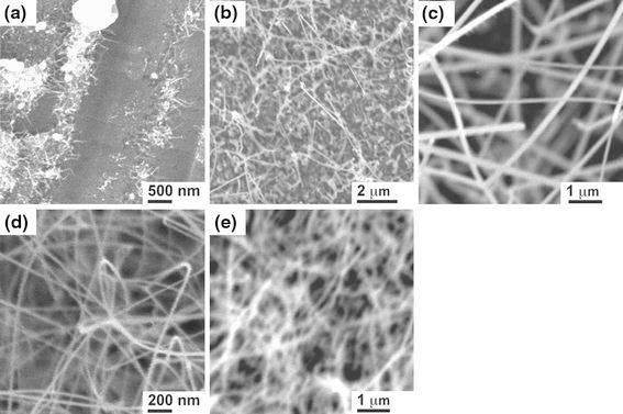
SEM images of ZnO nanostructures synthesized at a 910, b 930, c 940, d 950, and e 1,000°C for 100 min with Ar flow rate of 70 sccm at 760 Torr
Figure 4a shows the morphology of ZnO nanowires synthesized at 910°C. ZnO wire-like structures were grown at the edge of each nucleation site. The as-synthesized nanostructures were sparsely distributed on the FTO substrate surface with average lengths of 200–300 nm. When the synthesis was conducted at 930°C, as shown in Fig. 4b, typical nanowires with a higher aspect ratio can be found. The diameter ranged from 70 to 90 nm and length from 2 to 3 μm. With a further increase in reaction temperature, longer and higher density ZnO nanowires were synthesized. Figure 4c illustrates the morphology of the as-synthesized ZnO nanowires grown at 940°C. The ZnO nanowires have a diameter of 50–60 nm, and length of 3–4 μm, indicating that elevating the reaction temperature can form longer and thinner ZnO nanowires. The SEM image indicates that average distance between each single ZnO nanowire synthesized at 940°C is around 50–100 nm. Even denser and thinner ZnO nanowires have been synthesized at 950°C as shown in Fig. 4d. These nanowires have an average diameter of 30–50 nm.
ZnO nanowires were grown at temperatures as high as 1,000°C. Figure 4e reveals the typical morphology. Nanowires were closely spaced with the average wire-to-wire distance less than 120 nm. The average diameter was 30–50 nm, which is close to the size of the nanowires synthesized at 950°C, indicating the smallest diameter that can be achieved by elevating the growth temperature. The dependence of the nanowire average length and diameter on the growth temperature is shown in Fig. 5.
Figure 5.
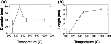
ZnO nanowire diameter and length measured as a function of maximum furnace temperature under fixed reaction conditions of: 100 min reaction time, 760 Torr, and Ar flow rate of 70 sccm
Effect of Flow Rate
The effect of carrier gas flow rate on the number density of synthesized ZnO nanowires has also been investigated. The experiments were conducted at carrier gas flow rates of 70, 139, and 200 sccm under the following fixed conditions: furnace temperature of 950°C, 100 min reaction time, and 760 Torr.
Figure 6a shows typical nanowires synthesized under a carrier gas flow rate of 139 sccm. It can be seen that only a few nanowires have been synthesized. Compared to the nanowires synthesized under a carrier gas flow rate of 70 sccm, the number density decreased significantly. ZnO nanoparticles rather than nanowires have been synthesized under a carrier gas flow rate of 200 sccm, as shown in Fig. 6b.
Figure 6.
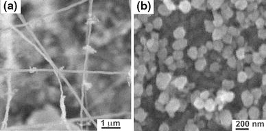
SEM images of a ZnO nanowires synthesized under argon gas flow rate of 139 sccm, b under 200 sccm
Chemical Composition and Structure
EDX data acquired from ZnO nanowires grown at 950°C are shown in Fig. 7. These confirm that the nanowires are composed of zinc and oxygen. The appearance of Si and Sn is due to the FTO glass substrate. The percentage of oxygen (59.78%) is approximately equal to the sum of three kinds of oxides: ZnO, SnO2, and SiO2 (60.15%). This result reveals that the main product is ZnO.
Figure 7.
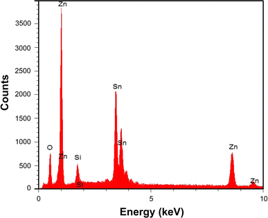
EDX analysis of nanowires grown at 950°C, 70 sccm Ar flow, at 760 Torr for 100 min showing that the nanowires are composed of Zn and O
X-ray diffraction further supported that the wires and nanoparticles were ZnO as well as the crystalline quality of the structures. The X-ray diffraction investigations showed that the FTO glass was highly textured, with its (200) axis being perpendicular to the substrate, as one can see in Fig. 8. To better distinguish the patterns acquired from the grown nanoparticles, offset (incidence angle close, but slightly different from theta) and grazing incidence (incidence angle = 5°) geometries were used, and the acquired patterns are displayed in Fig. 8. Also shown by vertical lines are the reference diffraction lines corresponding to standard ZnO (#36-1451 full line) and SnO2 (#41-1445 dotted line) powders [16]. One can note that there are no major differences between the offset and grazing incidence scans, which suggests that the grown ZnO particles are not textured. This is even more interesting taking into account the highly textured nature of the FTO glass and the propensity of ZnO to grow along its (002) axis when deposited from vapors [17]. This result confirms the SEM findings that the nucleation sites for ZnO particles were not located on the FTO film’s surface. The dimension of the crystalline grains, estimated from the full width at half maximum of the diffraction lines, which were corrected for instrumental broadening, was found to be around 22 nm.
Figure 8.
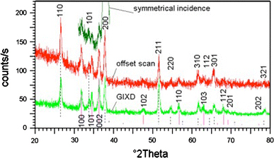
XRD patterns acquired from ZnO nanoparticles grown on FTO glass
Discussion
The present results of ZnO nanowire synthesis do not follow the conventional metal-catalytic vapor–liquid–solid (VLS) crystal growth mechanism [18]. Similar to previous studies [14,15] using a double-tube reactor configuration, the growth mechanism here can be described as a self-catalyzed and saturated VLS mechanism. This mechanism is depicted in Fig. 9.
Figure 9.
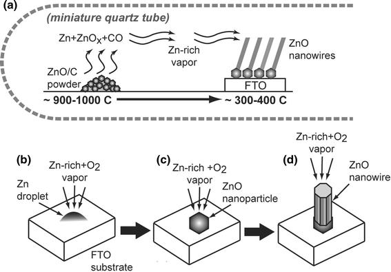
Diagram of self-catalyzed and saturated VLS crystal growth mechanism for ZnO nanowire synthesis in the miniature quartz tube reactor. ZnO/C undergo a carbothermal reduction a reaction at high temperature to produce Zn+ZnOx+CO vapors. These vapors are transported downstream and condense on the FTO glass substrate to form liquid Zn droplets (b) and ZnO nanoparticles (c). Further reaction time results in (d) adsorption and nucleation ZnO nanowires
At the closed-end of the miniature tube, carbothermal reduction of ZnO at 900–1,000°C (high temperature zone) resulted in Zn and ZnOx (suboxides) reaction products according to the following plausible mechanism:
 |
These products were transported in the vapor phase to the low-temperature zone (300–400°C). The role of the miniature tube is to confine the vapor thereby creating a highly concentrated Zn-rich vapor environment. During diffusion of the vapor across the lower temperature gradient, Zn and ZnOx reactants condense to form liquid droplets and/or particles that deposit on the FTO glass substrate. We note that the particle formation is a different mechanism as reported in previous double-tube studies where only liquid droplet formation and supersaturation is reported [14,15]. The SEM images in Fig. 2 show multilayer stacking of particles that is indicative of ZnO particle formation prior to deposition.
Upon further reaction time, the gaseous reactants adsorb on the ZnO nano- and meso- particles, which act as nucleation sites for 1D nanowire growth as shown in Fig. 2b. The crystal growth rate is determined by Zn and O2 vapor concentration ratio. ZnO nanowires can only be deposited when the Zn/O2 vapor concentration ratio reaches a critical value. Nanowire growth with the FTO acting as a metal catalyst is not likely since the melting temperature of SnO is ~1,080°C, which is not conducive to VLS crystal growth at the temperatures used here.
It can be seen from the presented SEM images that primarily growth temperature and time determine the morphology of as-synthesized nanostructures. ZnO nanowires grew at furnace temperatures above 930°C. Figure 5 illustrates the dependence of morphology of synthesized ZnO nanowires on growth temperature. Increasing temperature leads to the growth of longer and thinner nanowires. The smallest and longest nanowires have been synthesized at 1,000°C. The average diameter is around 40 nm, while the average length is greater than 5 μm.
In addition, the number density of as-synthesized ZnO nanowires is controlled by the growth temperature. Nanowires grown at higher temperatures have smaller wire-to-wire spacing, indicating denser nanowire growth.
SEM data indicated that the longer reaction time produced nanowires with longer length. Figure 3b illustrates the dependence of average length of synthesized ZnO nanowires on the reaction time. ZnO particles (rather than nanowires) were formed for reaction times less than 60 min. As the reaction time increased, the ZnO nanowires nucleate and grow from the ZnO particles. The longest nanowire is up to 5–6 μm in length.
Figure 3a illustrates the dependence of ZnO nanowire average diameter on the reaction time. A slight increase in the average ZnO nanowire diameter at longer reaction time is probably due to an increase in the size of nucleation sites during the growth. For the ZnO nanowires that started to grow after 80 min, the diameter for as-synthesized ZnO nanowires ranged from 35 to 60 nm.
Typical ZnO nanowires can be synthesized under a carrier gas flow rate around 70 sccm but higher flow rates yielded poor growth. If the gas flow is too high, the rate of Zn vapor diffusing from the inlet vial will be increased, it will degrade the Zn-rich environment; thereby decreasing nucleation of ZnO nanowires.
Conclusion
ZnO nanowires have been synthesized on FTO-coated glass substrates by a modified vapor transport deposition process using a double-tube reactor configuration. A parametric study has been conducted to investigate the effects of controllable reaction conditions in the synthesis process on nanowire size, morphology, and density. Growth occurs via a self-catalyzed and saturated VLS mechanism with the formation of ZnO nanoparticles that act as nucleation sites for synthesis of ZnO nanowires. ZnO nanowires can be synthesized with a growth time longer than 80 min, and the length of nanowires is mainly determined by the growth time. The longest nanowires have average length around 5.5 μm. ZnO nanowires cannot be formed unless the growth temperature at the precursor is higher than 930°C, while the average diameter and number density of nanowires array can be controlled by the growth temperature. SEM data indicated that nanowire diameters are inversely proportional to the growth temperature; the smallest nanowires can be obtained at 950–1,000°C and are around 40 nm in diameter. The ZnO nanowires made in this method have a wire diameter, length, and number density suitable for building hybrid metal oxide/organic solar cells on FTO-coated glass substrates as the substrate temperatures are less than 500°C.
Contributor Information
Dongshan Yu, Email: yds309@gmail.com.
Curtis R Taylor, Email: curtis.taylor@ufl.edu.
Acknowledgments
Microscopy was performed at the VCU Department of Anatomy and Neurobiology Microscopy Facility, supported, in part, with funding from NIH-NINDS Center core grant 5P30NS047463-02.
Open Access
This article is distributed under the terms of the Creative Commons Attribution Noncommercial License which permits any noncommercial use, distribution, and reproduction in any medium, provided the original author(s) and source are credited.
References
- Heo YW, Tien LC, Norton DP, Pearton SJ, Kang BS, Ren F, LaRoche JR. Appl. 2004. p. 15.
- Kind H, Yan H, Messer B, Law M, Yang P. Adv. 2002. p. 2.
- Peiro A, Ravirajan P, Govender K, Boyle D, O’brien P, Bradley D, Nelson J, Durrant J. J. 2006. p. 21.
- Fan ZY, Lu JG. Appl. 2005. p. 12.
- Beek W, Wienk M, Janssen R. Adv. 2004. p. 12. [DOI]
- Unalan H, Hiralal P, Kuo D, Parekh B, Amaratunga G, Chhowalla M. J. 2008. p. 48. [DOI]
- Coakley KM, McGehee MD. Chem. 2004. p. 23. [DOI]
- Baxter JB, Walker AM, van Ommering K, Aydil ES. Nanotechnology. 2006. p. 11. [DOI]
- Law M, Greene LE, Johnson JC, Saykally R, Yang P. Nat. 2005. p. 455. [DOI] [PubMed]
- Wang ZL. J. 2004. p. R829. [DOI]
- Feng XJ, Shankar K, Varghese OK, Paulose M, Latempa TJ, Grimes CA. Nano Lett. 2008. p. 11. [DOI] [PubMed]
- Xu C, Sun X, Dong Z, Yu M, My T, Zhang X, Chua S, White T. Nanotechnology. 2004. p. 7. [DOI]
- Du Pasquier A, Chen HH, Lu YC. Appl. 2006. p. 25. [DOI]
- Chang PC, Fan ZY, Wang DW, Tseng WY, Chiou WA, Hong J, Lu JG. Chem. 2004. p. 24.
- Geng C, Jiang Y, Yao Y, Meng X, Zapien J, Lee C, Lifshitz Y, Lee S. Adv. 2004. p. 6. [DOI]
- JCPDS-International Centre for Diffraction Data. 2009.
- Craciun V, Elders J, Gardeniers JE, Geretovsky J, Boyd IW. Thin Solid Films. 1995. p. 1. COI number [1:CAS:528:DyaK2MXkvFKrtLk%3D]; Bibcode number [1995TSF...259....1C] [DOI]
- Wagner RS, Ellis WC. Appl. 1964. p. 5. [DOI]


