Abstract
Solution-processed semiconductors are seen as a promising route to reducing the cost of the photovoltaic device manufacture. We are reporting a single-layer Schottky photovoltaic device that was fabricated by spin-coating intrinsic silicon nanocrystals (Si NCs) from colloidal suspension. The thin-film formation process was based on Si NCs without any ligand attachment, exchange, or removal reactions. The Schottky junction device showed a photovoltaic response with a power conversion efficiency of 0.02%, a fill factor of 0.26, short circuit-current density of 0.148 mA/cm2, and open-circuit voltage of 0.51 V.
Keywords: Silicon nanocrystals, Solar cell, Schottky junction, Thin film
Introduction
Although current commercial silicon solar cells can reach 10–20% power conversion efficiency (PCE), current solar cell manufacturing processes require high temperatures, vacuum technologies, and high-grade materials, all of which increase cost. As a result, current commercial solar cells remain expensive compared to fossil fuels, around 25–50 cents per kilowatt hour in the USA [1]. Organic solar cells, which are made from carbon-containing compounds, are usually made in solution so that they can be produced with low-cost printing or coating techniques. Liquid-phase coating processing can bring down manufacturing costs by avoiding high temperature and high vacuum methods. However, stability and carrier transport are challenges for organic solar cells. Current solar cells are expected to last for 20–30 years at temperatures between −20 and 90°C, which organic solar cells may not be able to achieve [2]. The highest carrier mobility in polymer-based organic solar cells is typically on the order of 0.1 cm2/Vs [3,4]. Compared to inorganic semiconductors, carrier mobility in organic solar cells is still low.
Colloidal nanocrystals have a number of attractive features for low-cost solar cells. Nanocrystal colloids offer the primary advantage of organic materials which lies in solution processability. Moreover, nanocrystals provide tunable broadband absorption and the photostability of traditional photovoltaic materials. Various promising nanocrystal-only solar cells have been reported, which were made by spin-coating or dip-coating nanocrystals onto substrates. Among the impressive demonstrations were devices which utilize cadmium selenide (CdSe) and cadmium telluride (CdTe) nanorods for heterojunction solar cells [5], which were found to be air stable. Lead selenide (PbSe) [6] and lead sulfide (PbS) [7] nanocrystals were used in Schottky junction solar cells. These devices are infrared harvesting and can utilize the broad solar spectrum. Although nanocrystal-only solar cells have shown encouraging efficiencies, cadmium, selenium, and lead are toxic materials that may limit their utility for large-scale deployment.
Silicon has dominated the solar cell market since the first crystalline silicon solar cell was reported to have a 6% power conversion efficiency by Chapin in 1954 [8].
Silicon is an abundant and non-toxic material, and it is also well studied in industrial applications. If this conventional material can be used in a novel way (e.g., nanocrystal solution processes), the manufacturing cost of silicon-based solar cells may be reduced. Here, we report a new thin-film formation process which may be applied in silicon-based photovoltaic devices using solution-processable silicon nanocrystals (Si NCs).
Experimental
By flowing and dissociating the precursor, silane (SiH4), 10–20 nm Si NCs were synthesized through a non-thermal plasma reactor under vacuum condition [9]. Five percent SiH4/Helium (He) was mixed with argon (Ar) and passed through a one inch outer diameter Pyrex tube with a copper electrode wrapped around it. The flow rate of 5% SiH4/He and Ar were 35 and 25 standard cubic centimeters per minute (SCCM), respectively. Radio frequency power of 175 Watts was applied to the electrodes at 13.56 MHz. The Si NCs were collected downstream of the plasma on stainless steel meshes. After Si NC deposition finished, the Si NCs were weighed and transferred to an air-tight vial (Sigma–Aldrich, 27150-U) inside a nitrogen-purged glove bag (oxygen level < 25 ppm).
In traditional colloidal nanocrystal synthesis, the surfaces of nanocrystals are passivated with coordinating ligands to provide solubility of nanocrystals in the solvents. After nanocrystal-film formation, the ligands are usually removed or exchanged with shorter ligands to enhance the interaction between nanocrystals. The presence of ligands, though required for solubility of the NCs, is an impediment, since it requires additional processing steps. Removal of the ligands may also cause detrimental cracking of the NC thin films, as the interparticle distance is reduced. However, in a previous study, we found that stable colloidal suspensions of Si NCs could be produced under certain solution conditions without the use of ligands attached to the NC surfaces [10]. Specifically, Si NCs were found to form stable suspensions in 1,2-dichlorobenzene. While agglomeration of Si NCs is not completely avoided by suspension in 1,2-dichlorobenze (DCB) and agglomerates sometimes of up to a micrometer in size were observed, the suspensions did not show significant precipitation over periods of several days.
It should be mentioned that, against common believe, the organic ligands around Si NCs are likely not essential in terminating surface defects such as dangling bonds. The surface of plasma synthesized Si NCs is largely covered with hydrogen, originating from the silian (SiH4) precursor used for plasma synthesis. In [12], we demonstrated that the surface coverage with hydrogen has a much more significant impact on the photoluminescence quantum yield and the dangling bond density of Si NCs than the coverage with organic ligands.
For the formation of Si NC colloids, the following protocol was used: DCB was dried with molecular sieves and degassed by bubbling nitrogen for 60 min in a Schlenk line to reduce the oxygen and moisture level. Si NCs were dispersed in DCB (ACROS) to form a cloudy, yet stable solution. The solution concentration was 8 mg Si NCs/ml DCB. To reduce Si NC agglomeration in the solution, the cloudy solution was sonicated for 20 min. The devices were fabricated by the spin-cast method immediately after sonication. The solution preparation process was conducted in a glove box (oxygen and moisture level < 1 ppm).
Device Fabrication
A Schottky junction solar cell is likely the simplest photovoltaic device that can be fabricated. While Schottky junction solar cells based on NC films with promising efficiencies were demonstrated based on PbSe [6] or PbS [7], to our knowledge, no prior demonstration of a Schottky junction solar cell based on Si NCs has been reported.
A scheme of the device architecture is shown in Fig. 1. To fabricate Si NC Schottky junction devices, Si NC thin films were spin-cast onto indium tin oxide (ITO)-coated glass substrates at 700 rpm in a glove box. To obtain the 250-nm Si NC thin film, several spin-coating steps were required. After Si NC deposition, devices were completed by the deposition of 100 nm of aluminum on the top of the film as the electrode. The active area of each device was 0.046 cm2.
Figure 1.

Schematic of a Si NC photovoltaic device
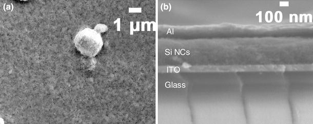
Spin-casting of Si NC suspension from DCB led to a rough and densely packed film, as shown by the scanning electron micrograph (SEM) in Fig. 2. The rough morphology was expected due to the agglomeration of Si NCs. It may negatively affect the device performance. Hence, further improvements in solubilizing Si NCs are desirable.
Figure 2.

SEM of Si NC photovoltaic devices. a Top view and b cross-section view
Results
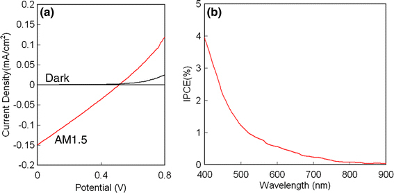
Solar cell devices were tested in an enclosure under dry nitrogen atmosphere in order to avoid the oxidation of the Si NCs, which was found to be detrimental for electron conduction through the Si NC films. There were six devices on one substrate; in this study, we found that one device short-circuited while the other five devices had similar performance. The current–voltage (I–V) of one device is shown in Fig. 3a. This device had a 0.02% PCE and a fill factor of 0.26, with short circuit-current density of 0.148 mA/cm2 and open-circuit voltage of 0.51 V. The other devices showed similar performance. The comparison to the I–V characteristic under dark conditions (i.e., without irradiation of the device) clearly shows that the device exhibits a photovoltaic effect. The fact that the I–V characteristic is almost linear in the forth quadrant suggests that the device has only a small shunt resistance, which would imply the electron–hole recombination is a significant loss channel in this device. This is not surprising, as the hydrogen-terminated surfaces of the Si NCs still provide surface trap states, which may act as recombination centers. The incident photon-to-current conversion efficiency (IPCE) for the Si NCs-only device is shown in Fig. 3b. As to be expected from the relatively poor performance of the device, the IPCE is relatively small with a maximum of ~ 4% in the ultraviolet.
Figure 3.

a Current–voltage characteristic (I–V) of a Si NC photovoltaic device. The I–V characteristic of the device was recorded under 100 mW/cm2 AM 1.5 global conditions and shows 0.02% PCE and a fill factor of 0.26 with 0.148 mA/cm2 short circuit-current density and 0.51 V open-circuit voltage. b Incident photon-to-current efficiency (IPCE) spectrum of the Si NC photovoltaic device
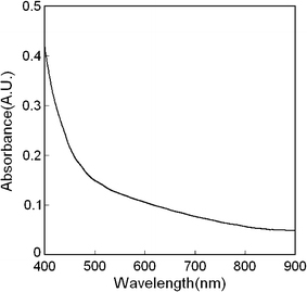
The optical absorption spectrum of Si NC-only films on the ITO substrate was measured and is displayed in Fig. 4. The IPCE trends of the Schottky photovoltaic device matched the absorption behavior of Si NC film. Figure 4 demonstrates that the Si NC film shows strong absorption only in the blue and ultraviolet range of the spectrum. While the Si NCs used here have a band gap only slightly larger than the Si bulk band gap of 1.1 eV, the absorption in the red-to-green range of the optical spectrum is poor. This is a consequence of the Si NCs still behaving as indirect band gap semiconductor material, a behavior that only breaks down once the Si NC size becomes smaller than ~2.5 nm [11]. However, it is unlikely that using smaller nanocrystals would provide any benefit for the performance of the devices. First, the optical absorption cross section of Si NCs was found to decrease with NC size, even for very small nanocrystals [13]. Second, the large increase in surface area and surface-related defects for smaller NCs and the presence of more grain boundaries would be an additional impediment to electron transport. For future studies, it may be interesting to study other means of increasing the absorption of the Si NCs, such as alloying silicon with germanium to for SixGe1−x NCs, which may show improved absorption [14].
Figure 4.

Room-temperature optical absorption spectrum of a Si NC film
Conclusions
In conclusion, the results of this study demonstrate that colloidal processing of non-functionalized Si NCs can be a new approach for silicon-based thin-film solar cell fabrication. Compared to the other nanocrystal thin-film formation processes, this process does not involve any attachment, exchange, or removal of ligands, which could reduce fabrication steps and cost. We demonstrated the first Si NC-only Schottky junction photovoltaic devices, which were successfully produced by spin-coating Si NC suspensions in an inert atmosphere. The devices show a clear photovoltaic response, which indicates that the Si NC thin film is continuous without short-circuiting problems. The performance of the photovoltaic devices was poor, likely due to poor absorption of radiation and significant charge carrier recombination. However, the results demonstrate the clear potential of solution-processed Si NCs for the low-cost formation of electronic devices such as solar cells and thin-film transistors.
Acknowledgments
This work was supported primarily by the MRSEC Program of the National Science Foundation under Award Number DMR-0819885. Partial support through NSF grant CBET-0500332 is acknowledged. During part of this work, C.Y.L. was supported by a University of Minnesota Doctoral Dissertation Fellowship. We utilized the University of Minnesota Characterization Facility which receives partial support from the NSF under the NNIN program.
Open Access
This article is distributed under the terms of the Creative Commons Attribution Noncommercial License which permits any noncommercial use, distribution, and reproduction in any medium, provided the original author(s) and source are credited.
References
- Lewis NS. MRS Bull. 2007. p. 808. [DOI]
- Antonio A, Hegedus S(eds.), editor. Handbook of Photovoltaic Science and Engineering. Wiley, Chichester; 2003. [Google Scholar]
- Chang J, Sun B, Breiby DW, Nielsen MM, Sölling TI, Giles M, McCulloch I, Sirringhaus H. Chem. 2004. p. 4772. COI number [1:CAS:528:DC%2BD2cXlslersL0%3D] [DOI]
- Sirringhaus H, Brown PJ, Friend RH, Nielsen MM, Bechgaard K, Langeveld-Voss BMW, Spiering AJH, Janssen RAJ, Meijer EW, Herwig P, de Leeuw DM. Nature. 1999. p. 685. COI number [1:CAS:528:DyaK1MXmvF2qsrg%3D]; Bibcode number [1999Natur.401..685S] [DOI]
- Gur I, Fromer NA, Geier ML, Alivisatos AP. Science. 2005. p. 462. COI number [1:CAS:528:DC%2BD2MXhtFahtr3I]; Bibcode number [2005Sci...310..462G] [DOI] [PubMed]
- Luther JM, Law M, Beard MC, Song Q, Reese MO, Ellingson RJ, Nozik AJ. Nano Lett. 2008. p. 3488. COI number [1:CAS:528:DC%2BD1cXhtValurnO]; Bibcode number [2008NanoL...8.3488L] [DOI] [PubMed]
- Johnston KW, Pattantyus-Abraham AG, Clifford JP, Myrskog SH, MacNeil DD, Levina L, Sargent EH. Appl. 2008. p. 151115. Bibcode number [2008ApPhL..92o1115J] [DOI]
- Chain DM, Fuller CS, Pearson GL. J. 1954. p. 676. Bibcode number [1954JAP....25..676C] [DOI]
- Mangolini L, Thimsen E, Kortshagen U. Nano Lett. 2005. p. 655. COI number [1:CAS:528:DC%2BD2MXitVSiurc%3D]; Bibcode number [2005NanoL...5..655M] [DOI] [PubMed]
- Liu CY, Holman ZC, Kortshagen U. Nano Lett. 2009. p. 449. COI number [1:CAS:528:DC%2BD1cXhsFCltL%2FM]; Bibcode number [2009NanoL...9..449L] [DOI] [PubMed]
- Sykora M, Mangolini L, Schaller RD, Kortshagen U, Jurbergs D, Klimov VI. Phys. 2008. pp. 6–067401. [DOI] [PubMed]
- Mangolini L, Kortshagen U. Adv. 2007. p. 2513. COI number [1:CAS:528:DC%2BD2sXhtFGhur%2FK] [DOI]
- Kovalev D, Diener J, Heckler H, Polisski G, Kunzner N, Koch F. Phys. Rev. B. 2000. p. 4485. COI number [1:CAS:528:DC%2BD3cXhtVGrsbw%3D]; Bibcode number [2000PhRvB..61.4485K] [DOI]
- Pi XD, Kortshagen U. Nanotechnology. 2009. p. 295602. COI number [1:STN:280:DC%2BD1Mvls1Gisw%3D%3D] [DOI] [PubMed]


