Abstract
In this paper, a simple method to synthesize silicon carbide (SiC) nanoribbons is presented. Silicon powder and carbon black powder placed in a horizontal tube furnace were exposed to temperatures ranging from 1,250 to 1,500°C for 5–12 h in an argon atmosphere at atmospheric pressure. The resulting SiC nanoribbons were tens to hundreds of microns in length, a few microns in width and tens of nanometers in thickness. The nanoribbons were characterized with electron microscopy, energy-dispersive X-ray spectroscopy, X-ray diffraction, Raman spectroscopy and X-ray photoelectron spectroscopy, and were found to be hexagonal wurtzite–type SiC (2H-SiC) with a growth direction of  . The influence of the synthesis conditions such as the reaction temperature, reaction duration and chamber pressure on the growth of the SiC nanomaterial was investigated. A vapor–solid reaction dominated nanoribbon growth mechanism was discussed.
Keywords: Silicon carbide, Nanomaterial synthesis, Nanoribbon, Nanobelt, Hexagonal wurtzite
Introduction
Silicon carbide (SiC) is a material with outstanding physical and mechanical properties. It has high mechanical strength, high hardness, low density, high thermal conductivity, low thermal expansion coefficient, large band-gap, and excellent oxidation and corrosion resistances [1-3]. It is a leading material for components and devices operating at high temperature, high power and under harsh environments [4,5]. Micro-sized SiC particles and whiskers are commonly used as reinforcement materials for ceramics, metals and alloys for various structural and tribological applications [6,7].
In the past decade, one-dimensional (1D) SiC nanostructures have been successfully synthesized. In 1995, Dai et al. [8] reported the first SiC nanorod synthesis by the reaction of carbon nanotubes with either silicon monoxide or silicon and iodine vapor. After that, a number of techniques have been developed to synthesize SiC nanowires, including the sol–gel [9], vapor–liquid–solid [10], vapor–solid [11], laser ablation [12] and chemical vapor deposition (CVD) [13] methods. More recently, SiC micro-/nanoribbons have been successfully synthesized by several research groups [14-16]. For instance, Xi et al. [15] reported the growth of cubic SiC (3C-SiC) nanobelts via the reaction of tetrachlorosilane, ethanol and lithium powder in an autoclave at low temperature (600°C) and suggested a lithium-assisted mechanism of SiC nanostructure growth. Yushin et al. [16] synthesized α-SiC micro-ribbons by a carbothermal reaction of silicon dioxide and graphite at high temperature (1,800–1,900°C). Wu et al. [14] reported the synthesis of bicrystalline SiC nanobelts via a thermal evaporation and condensation process with silicon powder and multi-wall carbon nanotubes as the raw materials at 1,250°C.
Compared with the bulk and micro-sized SiC structures, SiC nanostructures have several novel mechanical, electrical and optical properties as a result of their reduced size [17-21]. SiC nanowhiskers have been shown to have a much higher mechanical strength than SiC microwhiskers and bulk SiC. According to Wong et al. [17], SiC nanorod has an estimated yield strength of over 50 GPa, substantially higher than that of bulk SiC. Pan et al. [20] reported that SiC nanowires have a very low electron emission threshold and are thus promising for vacuum microelectronics application.
In this paper, we report a simple catalyst-free growth of crystalline SiC nanoribbons from powders of silicon and carbon black at high temperature (1,500°C). Detailed analyses by scanning electron microscopy (SEM), high-resolution transmission electron microscopy (HRTEM), energy-dispersive X-ray spectroscopy (EDX), X-ray powder diffraction (XRD), Raman spectroscopy and X-ray photoelectron spectroscopy (XPS) show that the nanoribbons are crystalline SiC with a hexagonal wurtzite structure (2H-SiC or α-SiC). Compared with other reported SiC nanobelt/ribbon synthesis methods, the main advantages of the current approach are the relatively low growth temperature and the catalyst-free synthesis.
Experimental Conditions
The synthesis of SiC nanoribbon was carried out in a home-built low-pressure CVD system. A schematic of the system is shown in Fig. 1. The reaction chamber is a high-purity alumina tube (40 mm o.d., 35 mm i.d., 700 mm in length) heated with a compact high-temperature tube furnace (GSL-1500, MTI Corp., Richmond, CA). The chamber pressure was monitored by a convection vacuum gauge (KJLC 275i, Kurt J. Lesker, Clairton, PA) and the gas flow rate was monitored by a mass flow meter (GFM 17, Aalborg, Orangeburg, NY). This system can be operated at a temperature range from room temperature to 1,500°C and over a pressure range from a few millitorr up to atmospheric (atm) pressure.
Figure 1.

Schematic of the system for silicon carbide nanomaterial synthesis
Silicon powder (200 nm–2 μm in diameter, 99.9985% purity, Alfa Aesar, Ward Hill, MA) and carbon black powder (~50 nm in diameter, 99.9% purity, Alfa Aesar, Ward Hill, MA) were used as the starting materials. The silicon powder was placed in the upstream and the carbon black powder in the downstream of an alumina boat (100 × 20 × 20 mm) with a silicon and carbon molar ratio of about 1:1. The alumina boat was then placed in the center of the reaction chamber (horizontal alumina tube). Before heating, the chamber was first evacuated to ~10 mTorr by a rotary vacuum pump. Then, the chamber pressure was adjusted to the desired pressure level with ultra pure argon (Ar) gas (99.999%, Airgas, Radnor, PA). After that, the chamber was ramped from room temperature to 1,500°C (center position temperature) at a rate of 10°C/min and was maintained at this temperature for desired reaction duration. Finally, the chamber was cooled down to room temperature at 10°C/min rate. A continuous flow of 200 sccm (standard cubic centimeters per minute) Ar gas was maintained during the entire process. After the reaction, grey colored powder was found in the carbon black powder section of the alumina boat.
The morphology of the as-synthesized SiC nanomaterial was observed under a SEM (7400F, JEOL, Tokyo, Japan) at an acceleration voltage of 15 kV. The chemical composition of the material was analyzed with EDX (NORAN System Six, Thermo Scientific, Waltham, MA) in the SEM. The nanomaterial was also observed under a HRTEM (CM200 FEG, Philips, Eindhoven, Netherlands) at 200 kV acceleration voltage for crystal structure determination and selected area electron diffraction (SAED) analysis. To prepare specimens for TEM observation, SiC nanomaterial was first dispersed in acetone by ultrasonication for 5 min. Then, a drop of the suspension was dipped onto a carbon-coated copper TEM grid. The crystallinity of the nanomaterial was characterized with XRD (AXS D8 FOCUS, Bruker, Germany) using a copper Kα1 (λ = 1.54 Å) radiation source. The Raman spectrum of the SiC nanomaterial was taken with a Raman spectrometer (514.5 nm excitation, Ar+ ion laser source, Renishaw invia, Gloucestershire, UK) at room temperature. XPS (PHI VersaProbe, Physical Electronics, MN) analysis was also performed on the SiC nanomaterial to characterize its chemical composition.
Results and Discussion
The SEM images of the as-grown SiC nanoribbons synthesized at 1,500°C under atmospheric pressure for 9 h reaction duration are shown in Fig. 2. The nanoribbons are over a hundred microns in length, a few microns in width and 30–100 nm in thickness. They have a relatively smooth surface with a centerline along the entire length (Fig. 2b).
Figure 2.
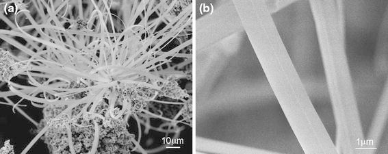
SEM images of a a nanoribbon cluster and b a nanoribbon segment
To determine the chemical composition of the nanoribbons, EDX measurements were performed in the SEM on several individual nanoribbons deposited on a copper substrate. Figure 3a shows one example where EDX signals were collected at both sides of a nanoribbon as well as the center region, and Fig. 3b shows a representative EDX spectrum collected from the left side of the nanoribbon. The EDX analysis indicated that the main composition of the nanoribbons is silicon and carbon. Small amount of aluminum, oxygen and copper were also detected. The aluminum and oxygen signals may come from the contamination of the alumina boat and the copper signal was contributed by the copper substrate. Table 1 summarizes the atomic percentages of silicon and carbon at the three locations marked in Fig. 3a. These results indicated that the chemical composition of the nanoribbon is uniform. The atom percentage of carbon is higher than that of ideal SiC, likely due to the contribution of residual hydrocarbon in the SEM vacuum chamber, which was confirmed by EDX analysis on the substrate.
Figure 3.
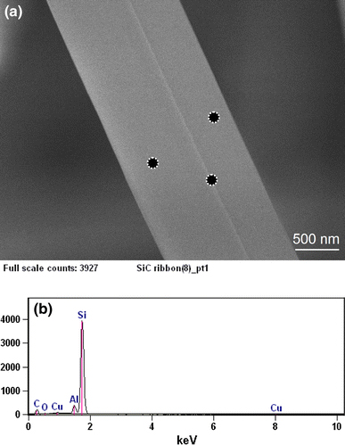
a SEM image of a nanoribbon segment with EDX signal collection spots marked; b EDX spectrum obtained from left side region of the nanoribbon
Table 1.
Atomic percentages of silicon and carbon at three regions of a SiC nanoribbon
| Location | Silicon (%) | Carbon (%) |
|---|---|---|
| Left | 22.3 | 74.7 |
| Center | 20.4 | 76.3 |
| Right | 21.7 | 75.5 |
The crystal structure of the SiC nanoribbons was investigated with a HRTEM, and Fig. 4a, 4b show low-resolution and high-resolution TEM images, respectively. As shown in Fig. 4b, the measured lattice spacing of the crystalline nanoribbon was 0.267 nm, indicating a  crystal growth direction. A SAED pattern recorded from the same area is shown in Fig. 4a (bottom insert), which confirmed that the nanoribbon is single crystalline and indicated that the growth direction is
  . While bicrystalline nanobelts with a twin boundary has been reported by several researchers [14,22,23], TEM observation at both sides of the nanoribbon revealed the same growth direction, indicating that such SiC nanoribbons do not have a bicrystalline structure and the centerline is not a twin boundary. Because of the greater thickness in the center region, the crystal structure of the centerline cannot be directly observed in TEM (Fig. 4a top insert). To further explore the structure of the center region, SAED was performed at both sides of the nanoribbon as well as at the centerline. The three regions were found to have identical SAED patterns, confirming that the centerline is not a twin boundary. A thin amorphous layer (1–2 nm) was also observed at the edge of the nanoribbons, which could be amorphous silica as reported by other researchers [24,25].
Figure 4.
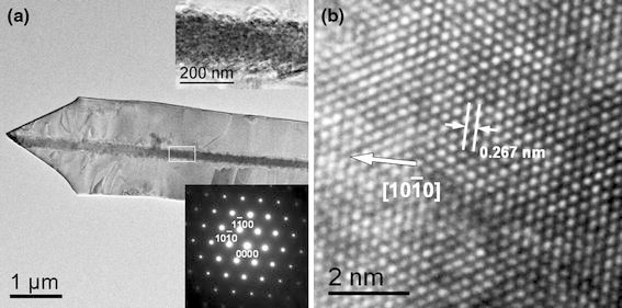
a TEM image of a silicon carbide nanoribbon segment (Topinsert: TEM image of the centerline region; Bottom insert: a representative SAED pattern); b HRTEM image showing crystal structure of the silicon carbide nanoribbon
A typical XRD pattern of the nanoribbons is shown in Fig. 5a. Most of the peaks are indexed as hexagonal 2H-SiC with a lattice parameter of a = 3.081 Å, in good agreement with the standard value (3.081Å, JCPDS Card No. 29-1126). The remaining peaks (labeled with stars in Fig. 5a) are assigned to the diffraction of ternary carbide compound (Al4SiC4), which could be a side product of the SiC synthesis process via the reaction of aluminum, carbon black and SiC at high temperature [26,27].
Figure 5.
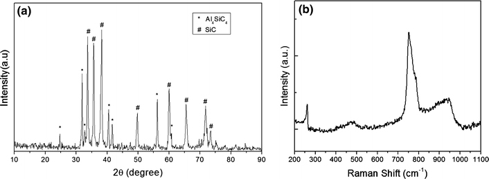
a XRD pattern and b Raman spectrum of silicon carbide nanoribbons
Figure 5b shows a typical Raman spectrum (200–1,100 cm−1) of the SiC nanoribbons. Raman peaks at around 260, 752, 786 and 946 cm−1 are observed that correspond to the peaks of 2H-SiC. The peak at 260 cm−1 is attributed to the transverse acoustic (TA) mode, the peaks at 752 and 786 cm−1 correspond to the transverse optical (TO) mode, and the peak at 946 cm−1 is the characteristic of longitudinal optical (LO) mode. The reported Raman peaks of bulk 2H-SiC are 264, 764, 799 and 968 cm−1[28]. The SiC nanoribbon sample has a frequency shift of ~4–22 cm−1, which could be the result of size confinement and/or the presence of structural defects [29,30].
An XPS spectrum of the SiC nanoribbons is shown in Fig. 6a and an enlarged carbon peak (C1s) spectrum is shown in Fig. 6b. The strong peak near 283.3 eV clearly indicates the existence of carbide bonding [31,32], and the weaker peak near 287 eV indicates the presence of residual graphitic carbon. The aluminum peak is believed to be contamination from the alumina boat, which has also been detected in the EDX and XRD analyses. The oxygen peak could be a combination of alumina contamination and the oxidation of the SiC and residual carbon black.
Figure 6.
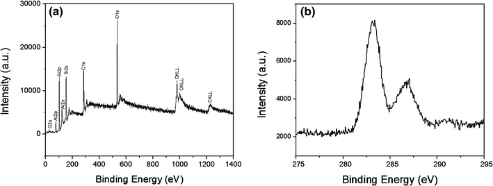
a XPS spectrum and b detailed C1s spectrum of the silicon nanoribbons
The synthesis conditions such as the reaction temperature, reaction duration and chamber pressure can have significant effects on the morphology and structure of the resulting SiC nanomaterial [33,34]. A series of experiments were carried out to systematically explore the effects of the three reaction parameters: (1) Reaction temperature effect: the center position temperature of the tube furnace was varied from 1,250 to 1,500°C (maximum allowable temperature of the system) with an interval of 50°C at a chamber pressure of 1 atm for 9-h reaction duration with a 200 sccm continuous flow of Ar gas. Due to the limitation of the tube furnace, we were not able to explore the reaction temperature effect above 1,500°C. Figure 7a–7f show SEM images of the nanostructures synthesized at 1,250, 1,300, 1,350, 1,400, 1,450 and 1,500°C, respectively. No evidence of reaction was observed for synthesis at 1,250°C, which is much lower than the melting point of bulk silicon. Microcrystals and needle-like structures were observed on carbon black powder surface for reactions at 1,300 and 1,350°C. For reactions at 1,400°C and above, ribbon structures were observed. Also, the lengths of the nanostructures synthesized above 1,400°C were much longer than those of the ones synthesized below 1,400°C, most likely due to the increased supply of silicon vapor at higher temperature.
Figure 7.
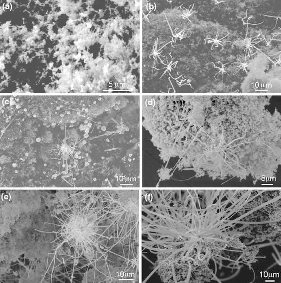
SEM images of nanomaterials synthesized at different reaction temperatures: a 1,250°C; b 1,300°C; c 1,350°C; d 1,400°C; e 1,450°C and f 1,500°C with 9-h reaction duration at atmospheric pressure
(2) Reaction duration effect: A series of synthesis trials were carried out with the reaction time of 5, 6, 9, 10.5 and 12 h at 1,500°C reaction temperature and 1 atm chamber pressure with a 200 sccm continuous flow of Ar gas. Figure 8a–8d show the SEM images of the nanostructures synthesized with 5-, 6-, 9- and 10.5-h reaction duration, respectively. For 5-h reaction duration, a number of SiC micro-/nanocrystals were observed on the surface of the carbon black powder. For 6-h reaction duration, small clusters of SiC nanoribbons were observed, which appeared to grow from the SiC micro-/nanocrystals on the carbon black powder surface. With increasing reaction duration, the length of the nanoribbons increased while their width remained roughly the same. To quantify the dependence of nanoribbon length on the reaction duration, we randomly picked a number of ribbons in the recorded SEM images and measured their lengths. The resulting relationship between the nanoribbon length and the reaction duration appeared to be linear, with a projected nanoribbon growth initiation at ~5.5 h reaction duration.
Figure 8.
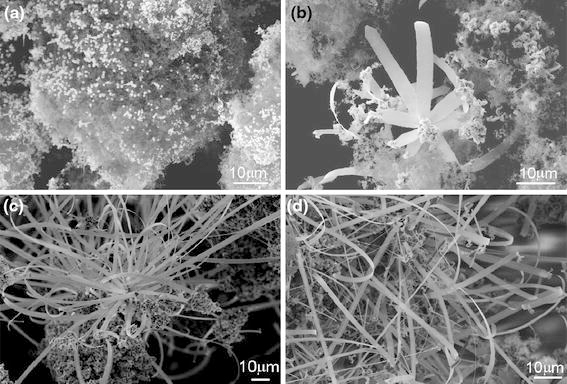
SEM images of nanomaterials synthesized with different reaction durations: a 5 h; b 6 h; c 9 h and d 10.5 h at 1,500°C reaction temperature and atmospheric pressure
(3) Chamber pressure effect: We briefly explored the influence of the chamber pressure on the SiC nanostructure growth by performing synthesis trials at 1.5 torr and 1 atm pressure at 1,500°C for 9 h with a 200 sccm continuous flow of Ar gas. At 1.5 torr pressure, micro-sized silicon needles were observed in the region where silicon powder was located, but no SiC nanomaterial was observed in the carbon black region. Such observation indicates that the chamber pressure is a critical parameter for the reaction of silicon vapor with carbon black. However, due to the limitation of our current home-built CVD system, we were not able to explore the chamber pressure effect over a wide range of pressure levels.
The catalyst-free thermal evaporation growth has been previously reported by several researchers for the synthesis of SiC nanowhiskers and nanobelts [14,34-36]. Because the carbon black powder is physically separated from the silicon powder in the alumina boat, the growth of the SiC nanoribbon in carbon black powder region is believed to be dominated by the reaction of the solid carbon with silicon vapor (vapor–solid mechanism) rather than the reaction of solid carbon with liquid silicon (vapor–liquid–solid mechanism). Synthesis trials were carried out with mixed silicon and carbon black powders under the same reaction condition (1,500°C, 9 h, 1 atm, 200 sccm continuous Ar flow). Randomly oriented submicron- and micron-sized SiC polycrystals were observed in the resulting material without any evidence of nanoribbon growth.
Based on the SiC synthesis condition study, we propose the following vapor–solid growth mechanism, as illustrated in Fig. 9. First, the silicon powder is melted and vaporized at elevated temperature (probably around 1,300°C, below the melting point of bulk silicon, 1,410°C), and the silicon vapor is transported downstream to the carbon black powder region by the Ar gas flow. Then, the silicon vapor reacts with carbon and forms SiC nuclei on the surface of the carbon black powder, possible assisted by the impurity oxygen in Ar gas as recently proposed by Wu et al. [33]. Such SiC nuclei gradually grow into micron-sized SiC crystals as shown in Fig. 8a. With further increase in the reaction time, nanoribbon clusters start to grow from the surfaces of the SiC microcrystals, and their lengths increase linearly with the reaction time. It is unclear what initiates the growth of nanoribbons from the microcrystals, which seems to relate to the reaction temperature and silicon vapor supply. At low reaction temperature, i.e., 1,300–1,400°C, only short SiC needles and whiskers are formed on the SiC microcrystals. Above the melting point of silicon, increased supply of silicon vapor appears to favor the growth of nanoribbons.
Figure 9.
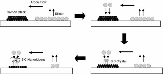
Schematic of the vapor–solid growth of SiC nanoribbons
Conclusion
In summary, SiC nanoribbons were synthesized by a reaction of silicon vapor and carbon black powder at 1,500°C in Ar atmosphere at atmospheric pressure. The nanoribbons were typically tens to hundreds of microns in length, several microns in width and tens of nanometers in thickness. The nanoribbons were characterized with SEM, HRTEM, EDX, XRD, Raman spectroscopy and XPS, and were found to be hexagonal 2H-SiC with a growth direction of  . The influence of synthesis conditions including the reaction temperature, reaction duration and chamber pressure on the growth of the SiC nanomaterials was investigated. The reaction temperature was varied from 1,250 to 1,500°C, and the nanoribbon growth was observed for reactions above 1,400°C. The reaction duration was varied from 5 to 12 h, and the nanoribbons were found to start growing at ~5.5-h reaction duration, with their lengths increasing almost linearly with the reaction duration. Reactions were carried out at 1.5 torr and 1 atm chamber pressures, and no nanoribbon growth was observed at 1.5 torr pressure. Based on the synthesis condition study, a vapor–solid reaction dominated growth mechanism was proposed for the SiC nanoribbon growth.
Acknowledgments
W. Ding appreciates the support of the start-up fund at Clarkson University. We are grateful to the Center for Advanced Materials Processing (CAMP) at Clarkson, the John M. Cowley Center for High Resolution Electron Microscopy at Arizona State University and the Nanosystem Engineering System Facility and Equipment Resources at West Virginia University for supplying multi-user facilities used in this work.
Open Access
This article is distributed under the terms of the Creative Commons Attribution Noncommercial License which permits any noncommercial use, distribution, and reproduction in any medium, provided the original author(s) and source are credited.
References
- Narushima T, Goto T, Hirai T, Iguchi Y. Mater. Trans. JIM. 1997. p. 821. COI number [1:CAS:528:DyaK1cXktFGltg%3D%3D]
- Wang SZ, Xu LY, Shu BY, Xiao B, Zhuang JY, Shi EW. J. 1999. p. 527. COI number [1:CAS:528:DyaK1MXlvF2ntL0%3D]
- Watari K. J. Ceram. Soc. Japan. 2001. p. S7. COI number [1:CAS:528:DC%2BD3MXpsVWqtg%3D%3D]
- Mehregany M, Zorman CA, Roy S, Fleischman AJ, Wu CH, Rajan N. Int. 2000. p. 85. COI number [1:CAS:528:DC%2BD3cXovFaht78%3D] [DOI]
- Willander M, Friesel M, Wahab QU, Straumal B. J. 2006. p. 1. COI number [1:CAS:528:DC%2BD2MXhtlWrs7zF] [DOI]
- Wang DZ, Peng HX, Liu J, Yao CK, Han H. Comp. 1995. p. 21. COI number [1:CAS:528:DyaK2MXlvVOgsbc%3D] [DOI]
- Garcia I, Fransaer J, Celis JP. Surf. 2001. p. 171. COI number [1:CAS:528:DC%2BD3MXnvFWmtrk%3D] [DOI]
- Dai HJ, Wong EW, Lu YZ, Fan SS, Lieber CM. Nature. 1995. p. 769. COI number [1:CAS:528:DyaK2MXmvVymtbk%3D]; Bibcode number [1995Natur.375..769D] [DOI]
- Meng GW, Zhang LD, Mo CM, Zhang SY, Qin Y, Feng SP, Li HJ. J. 1998. p. 2533. COI number [1:CAS:528:DyaK1cXlvFKntb4%3D]; Bibcode number [1998JMatR..13.2533M] [DOI]
- Deng SZ, Wu ZS, Zhou J, Xu NS, Chen R, Chen J. J. 2002. p. 511. COI number [1:CAS:528:DC%2BD38Xjt1Gqt7c%3D]; Bibcode number [2002CPL...356..511D] [DOI]
- Niu JJ, Wang JN, Xu QF. Langmuir. 2008. p. 6918. COI number [1:CAS:528:DC%2BD1cXms1agt78%3D] [DOI] [PubMed]
- Shi WS, Zheng YF, Peng HY, Wang N, Lee CS, Lee ST. J. 2000. p. 3228. COI number [1:CAS:528:DC%2BD3MXps1Cm] [DOI]
- Wei J, Li KZ, Li HJ, Fu QG, Zhang L. Mater. 2006. p. 140. COI number [1:CAS:528:DC%2BD2MXhtVOlur3O] [DOI]
- Wu RB, Wu LL, Yang GY, Pan Y, Chen JJ, Zhai R, Lin J. J. 2007. p. 3697. COI number [1:CAS:528:DC%2BD2sXntlyruro%3D]; Bibcode number [2007JPhD...40.3697W] [DOI]
- Xi GC, Peng YY, Wan SM, Li TW, Yu WC, Qian YT. J. Phys. Chem. B. 2004. p. 20102. COI number [1:CAS:528:DC%2BD2cXhtVSmt77K] [DOI]
- Yushin GN, Cambaz ZG, Gogotsi Y, Vyshnyakova KL, Pereselentseva LN. J. 2008. p. 83. COI number [1:CAS:528:DC%2BD1cXht1OjsL8%3D] [DOI]
- Wong EW, Sheehan PE, Lieber CM. Science. 1997. p. 1971. COI number [1:CAS:528:DyaK2sXmt12ku7k%3D] [DOI]
- Han XD, Zhang YF, Zheng K, Zhang XN, Zhang Z, Hao YJ, Guo XY, Yuan J, Wang ZL. Nano Lett. 2007. p. 452. COI number [1:CAS:528:DC%2BD28XhtlGku7rJ]; Bibcode number [2007NanoL...7..452H] [DOI] [PubMed]
- Shim HW, Kuppers JD, Huang HC. Nanotechnology. 2009. p. 025704. COI number [1:CAS:528:DC%2BD1MXjtFGhsbw%3D]; Bibcode number [2009Nanot..20b5704S] [DOI] [PubMed]
- Pan ZW, Lai HL, Au FCK, Duan XF, Zhou WY, Shi WS, Wang N, Lee CS, Wong NB, Lee ST, Xie SS. Adv. 2000. p. 1186. COI number [1:CAS:528:DC%2BD3cXmsFSksrw%3D] [DOI]
- Deng SZ, Li ZB, Wang WL, Xu NS, Zhou J, Zheng XG, Xu HT, Chen J, She JC. Appl. 2006. p. 023118. COI number [1:CAS:528:DC%2BD28XnsFeju7Y%3D]; Bibcode number [2006ApPhL..89b3118D] [DOI]
- Fan X, Zhang ML, Shafiq I, Zhang WJ, Lee CS, Lee ST. Cryst. 2009. p. 1375. COI number [1:CAS:528:DC%2BD1MXlvFyjtQ%3D%3D] [DOI]
- Chun HJ, Choi YS, Bae SY, Park J. Appl. 2005. p. 539. COI number [1:CAS:528:DC%2BD2MXltlSmu7g%3D]; Bibcode number [2005ApPhA..81..539C] [DOI]
- Yang GZ, Cui H, Sun Y, Gong L, Chen J, Jiang D, Wang CX. J. Phys. Chem. C. 2009. p. 15969. COI number [1:CAS:528:DC%2BD1MXpslahs7s%3D] [DOI]
- Yang GY, Wu RB, Chen JJ, Pan Y, Zhai R, Wu LL, Lin J. Nanotechnology. 2007. p. 155601. COI number [1:CAS:528:DC%2BD2sXmtVCnsb4%3D]; Bibcode number [2007Nanot..18o5601Y] [DOI]
- Huang XX, Wen GW. Mater. 2006. pp. 193–199. COI number [1:CAS:528:DC%2BD28Xit1Wku7w%3D] [DOI]
- Lee JS, Nishimura T, Tanaka H, Lee SH. In: in Synthesis of single-phase, hexagonal plate-like Al 4SiC4 powder, in siaions and non-oxides. ed. by K. Komeya, Y.B. Cheng, J. Tatami, and M. Mitomo, editor. Trans Tech Publications Ltd, Stafa-Zurich; 2009. p. 159. [Google Scholar]
- Bechelany M, Brioude A, Cornu D, Ferro G, Miele P. Adv. 2007. p. 939. COI number [1:CAS:528:DC%2BD2sXlsV2itLw%3D] [DOI]
- Zhang SL, Zhu BF, Huang FM, Yan Y, Shang EY, Fan SS, Han WG. Sol. 1999. p. 647. COI number [1:CAS:528:DyaK1MXlslWisrg%3D]; Bibcode number [1999SSCom.111..647Z] [DOI]
- Yao Y, Lee ST, Li FH. Chem. 2003. p. 628. COI number [1:CAS:528:DC%2BD3sXptVWgsr0%3D]; Bibcode number [2003CPL...381..628Y] [DOI]
- Gupta A, Paramanik D, Varma S, Jacob C. Bull. 2004. p. 445. COI number [1:CAS:528:DC%2BD2cXovFCqsr8%3D] [DOI]
- Liu XQ, Lin T, Shao HP, Guo ZM, Luo J, Hao JJ. Rare Metals. 2008. p. 320. COI number [1:CAS:528:DC%2BD1cXovVSmsro%3D] [DOI]
- Wu RB, Li BS, Gao MX, Chen JJ, Zhu QM, Pan Y. Nanotechnology. 2008. p. 335602. COI number [1:CAS:528:DC%2BD1cXhtF2qurfE]; Bibcode number [2008Nanot..19A5602W] [DOI] [PubMed]
- Wu RB, Yang GY, Pan Y, Chen JJ, Zhai R, Wu LL, Lin J. J. 2008. p. 241. COI number [1:CAS:528:DC%2BD1cXjtV2rt78%3D] [DOI]
- Yang GY, Wu RB, Pan Y, Chen JJ, Zhai R, Wu LL, Lin J. Physica E Low Dimens. 2007. p. 171. COI number [1:CAS:528:DC%2BD2sXmvVGhs7Y%3D]; Bibcode number [2007PhyE...39..171Y] [DOI]
- Wu RB, Yang GY, Pan Y, Chen JJ. Appl. 2007. p. 271. COI number [1:CAS:528:DC%2BD28Xht1KisLzF]; Bibcode number [2007ApPhA..86..271W]


