Abstract
A hybrid integrated circuit (IC) / microfluidic chip is presented that independently and simultaneously traps and moves microscopic objects suspended in fluid using both electric and magnetic fields. This hybrid chip controls the location of dielectric objects, such as living cells and drops of fluid, on a 60 × 61 array of pixels that are 30 × 38 μm2 in size, each of which can be individually addressed with a 50 V peak-to-peak, DC to 10 MHz radio frequency voltage. These high voltage pixels produce electric fields above the chip’s surface with a magnitude  , resulting in strong dielectrophoresis (DEP) forces
  . Underneath the array of DEP pixels there is a magnetic matrix that consists of two perpendicular sets of 60 metal wires running across the chip. Each wire can be sourced with 120 mA to trap and move magnetically susceptible objects using magnetophoresis (MP). The DEP pixel array and magnetic matrix can be used simultaneously to apply forces to microscopic objects, such as living cells or lipid vesicles, that are tagged with magnetic nanoparticles. The capabilities of the hybrid IC / microfluidic chip demonstrated in this paper provide important building blocks for a platform for biological and chemical applications.
Keywords: Lab-on-a-chip, Hybrid Integrated Circuit / Microfluidic, Dielectrophoresis, Magnetophoresis, Vesicle
I. Introduction
The complexity, small feature size, and low cost of integrated circuits (ICs) can be applied to biological and chemical applications by combining ICs with microfluidics to form hybrid IC / microfluidic chips.1 On these chips microscopic objects suspended in fluid can be controlled using spatially patterned electric and magnetic fields created above the IC’s surface.1-7 The small feature size and complexity of ICs enable these hybrid IC / microfluidic chips to have parallel control over many microscopic objects, such as individual living cells and small volumes of fluid.1 A motivation for this technology is to miniaturize the chemical and biological tasks performed in laboratories onto automated and inexpensive chips, which have applications in point-of-care medicine, environmental sensing, and in bringing medical diagnostics to the developing world.1,8,9
Previously developed hybrid IC / microfluidic chips control microscopic objects suspended in fluid using either electric or magnetic fields. Hybrid chips have been demonstrated that create spatially patterned electric fields to control the position of pL drops of fluid6 and living cells5,6 using dielectrophoresis (DEP). Chips have also been demonstrated that create spatially patterned magnetic fields using matrixes of wires7 and arrays of microcoils4 to trap and position biological objects tagged by magnetic nanoparticles using magnetophoresis (MP). In addition, magnetic nanoparticles can be functionalized to bind to specific locations inside of living cells and have been used to apply precise mechanical stresses on cell membranes10 and to control individual ion channels and surface receptors.11
In this paper, a hybrid IC / microfluidic chip is described that can simultaneously control objects using both DEP and MP. Dielectrophoresis can be used to trap and position living cells and small volumes of fluid. Magnetophoresis can be used to trap and move objects tagged with magnetic nanoparticles. In addition, the hybrid chip can use DEP and MP simultaneously to apply forces to dielectric objects that are tagged with magnetic nanoparticles. Unilamellar lipid vesicles are used as pL volume containers for fluids on the chip. The vesicles can be suspended in biologically-compatible aqueous solutions and are impermeable and stable for a wide range of salinity, pH, and other environmental conditions.12,13 The chip’s capabilities are demonstrated by using DEP to position picoliter (pL) volumes of fluid packaged in micrometer-sized lipid vesicles and by using MP to position iron-oxide beads. In addition, DEP and MP are used together to deform lipid vesicles with iron-oxide nanoparticles inside.
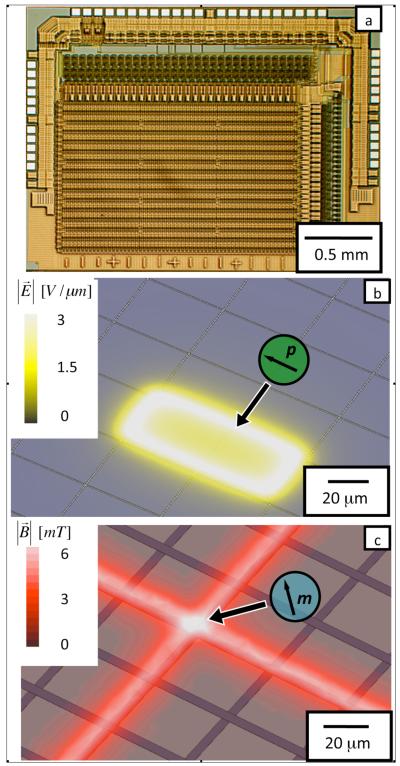
The hybrid chip consists of a custom IC that is fabricated in a commercial foundry and a fluid chamber that is built directly on top of it at Harvard. The IC, as is shown in an optical micrograph in Fig. 1a, includes an array of metal pixels that can each be addressed with a radio frequency (RF) voltage to locally apply DEP forces, a matrix of wires that runs underneath the DEP pixel array to apply local MP forces, and integrated sensors to locally report the temperature of the chip. The large array of DEP pixels, magnetic wires, and temperature sensors are controlled using static random access memory (SRAM) and logic that are built into the IC.
Fig. 1.
a. A micrograph of the integrated circuit. b. The magnitude of the electric field  from a quasi-static electric field simulation is plotted 5 μm above the chip surface. The pixels are shown as blue tiles that cover the surface of the chip. Two pixels are held at 50 V relative to the surrounding pixels. c. The magnitude of the magnetic field
  from simulation is plotted 5 μm above the chip’s surface. The wires are shown as blue stripes running across the surface of the chip. Two wires are sourced with 120 mA and all surrounding wires set to 0 mA.
II. Methods
The hybrid chip creates electric fields above its surface with a 2D array of metal pixels that can each be addressed with a radio frequency (RF) voltage. The array consists of 60 × 61 pixels that are 30 × 38 μm2 in size, which can each be individually driven with a 50 V peak-to-peak voltage at frequencies from DC to 10 MHz. The gap between pixels is 0.8 μm. The field generated 5 μm above the chip’s surface from two pixels held at 50 V relative to the surrounding pixels is shown in Fig. 1b. The electric field strength has a maximum value . The electric field is calculated using an electrostatic finite element simulation. (Maxwell 11, Ansoft)
The chip uses RF electric fields to trap and move dielectric objects, such as cells or pL volumes of fluid. Dielectrophoresis is the motion of a dielectric object in a non-uniform electric field. A spherical object in an electric field experiences a force given by the expression:6
| (1) |
where a is the radius of the particle, ηm′ is the real part of the permittivity of the medium, and ω is the frequency of the applied electric field. The Clausius-Mossotti factor is a function of the frequency dependent complex permittivity of the particle and the medium . A cell or vesicle with a radius a = 5 μm, suspended in a deionized glucose solution experiences a force towards the activated pixels, as is shown in Fig. 1b. A vesicle filled with saline solution has dielectric properties similar to that of a living cell at MHz frequencies and thus can be controlled with DEP.12
Underneath the array of DEP pixels is a magnetic matrix that consists of two perpendicular sets of 60 metal wires that run across the chip. The wires can be individually sourced with ±120 mA or 0 mA to apply forces on magnetically susceptible objects above the chip’s surface. The field, 5 μm above the IC’s surface, generated from two perpendicular wires each driven with 120 mA is shown in Fig. 1c. The magnetic field strength has a maximum value of that occurs at the point where the two activated wires cross. The magnetic field is calculated with a magnetostatic finite element simulation. (Maxwell 11, Ansoft)
The chip uses magnetic fields to trap and move objects with magnetic susceptibility different than that of the surrounding medium. Magnetophoresis is the motion of a magnetically susceptible object in a non-uniform magnetic field. A spherical object in a magnetic field experiences a force given by the expression:7
| (2) |
where a is the radius of the particle, χ is the linear magnetic susceptibility of the particle relative to the medium, and μ0 is the vacuum permeability. An iron-oxide bead with a radius a = 1 μm (Bioclone: FF102) will experience a force towards the maximum of the magnetic field, at the point where the two activated wires intersect. Current can be driven through several wires in the matrix simultaneously to create more than one field maximum, allowing the chip to trap and move many magnetic objects independently.7
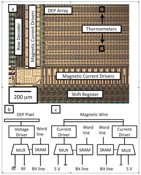
Figure 2a shows an optical micrograph of a section of the chip that shows the DEP pixel array, the current drivers for the magnetic matrix, and the digital logic that is used to update and read from the array. The chip’s large array of DEP pixels (3,660 total pixels), magnetic matrix (120 wires), and 16 distributed temperature sensors are addressed with logic and memory built into the IC, such that only 6 digital data lines are required to update the entire chip. The state of the chip is stored in an integrated SRAM memory that controls the DEP pixels, magnetic wires, and addresses the temperature sensors.
Fig. 2.
a. A micrograph of a part of the integrated circuit showing the DEP array, the magnetic current drivers, and the logic and memory used to update the SRAM array. b. A schematic of the circuitry underneath each DEP pixel, showing the SRAM memory element, and a multiplexer (MUX) that directs either the RF signal or its logical inverse to a voltage driver that connects to the electrode. c. A schematic of the circuitry for each magnetic wire in the matrix, showing the SRAM memory elements and the MUXs that connect to the current drivers to drive the wires with either ±120 mA or 0 mA.
There is an SRAM element underneath each DEP pixel, each temperature sensor, and each current driver for the magnetic wires. The SRAM array is organized into 32 words that each has 128 bits. The memory array is updated by selecting a word-line and then loading its state using a 128-bit shift register. The shift register uses a two-phase clocking scheme. Word selection is done with a standard 5-bit row decoder. The entire SRAM array can be updated at a rate of ~50Hz and individual words in the SRAM can be updated at a rate of ~1.5 kHz.
A schematic for the circuit underneath each DEP pixel is shown in Fig. 2b. The state of the SRAM memory element controls a 2:1 multiplexer (MUX) that directs either the RF signal or its logical inverse to a voltage driving circuit that connects to the pixel. A schematic for each magnetic line is shown in Fig. 2c. The magnetic lines have driving circuitry on both ends. Each wires can be driven with ±120 mA or 0 mA by setting the memory elements on the current drivers. Interspersed throughout the array are 16 distributed temperature sensors that can be individually addressed to be routed to an analog voltage output corresponding to the local temperature.
The IC was designed at Harvard using Cadence Design Software (Cadence) and fabricated in a commercial foundry on a high voltage 0.6 μm process (X-Fab – XC06 MIDOX). A fluid cell is built directly on top of the IC with a silicone gasket (Invitrogen: p-24744) with a 1.2 mm hole cut out with a hole-punch. A 3 × 3 mm2 glass cover slip seals the fluid cell. The device sits on a chip carrier on a custom printed circuit board connected to a computer through a digital input / output card (National Instruments: PCI-6254). The patterns sent to the chip are created using a graphical user interface written in MATLAB (The MathWorks) and sent to the PCI card with a custom Labview (National Instruments) program. The device sits under an Olympus fluorescence microscope with a digital camera (Hammamatsu: Orca-ER).
The vesicles are prepared with liposome electroformation using a modification of the Angelova method.14 The unilamellar vesicles are loaded with 4mM NaCl and suspended in a glucose solution, which provides contrast in the complex dielectric response to facilitate DEP and balances the osmotic pressure.6 The vesicles’ membranes are stained with rhodamine such that the vesicles are easily observable under a fluorescence microscope.
III. Results
The chip’s ability to control microscopic objects using both DEP and MP is demonstrated in this section. Unilamellar vesicles suspended in a deionized glucose solution are trapped and positioned using the DEP pixel array. Iron oxide beads are trapped and moved using the magnetic matrix. The utility of combining electric and magnetic forces on the same chip is demonstrated by deforming vesicles tagged with iron-oxide nanoparticles using the DEP pixel array and the magnetic matrix together.
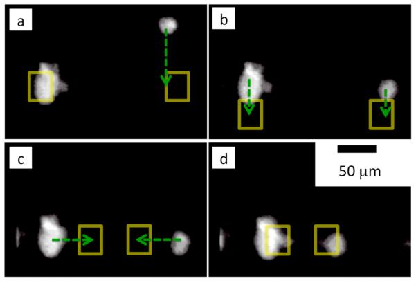
Individual vesicles are trapped and moved along programmed paths using the DEP pixel array. Figure 3 shows two vesicles that are independently trapped on the chip with DEP pixels. In Fig. 3(a-d) the vesicles are trapped and moved at speeds up to 80 μm/sec by sequentially changing the pixels that are turned on. In Fig. 3a the vesicle on the right is independently moved downwards while the vesicle on the left is held in place. In Fig. 3b both the left and right vesicle are moved downwards simultaneously. In Fig. 3c the vesicle on the left is moved to the right while the vesicle to the right is simultaneously moved to the left. The chip has 3,660 pixels and the entire array can be refreshed at ~50 Hz, enabling many individual vesicles to be controlled simultaneously. The ability to trap and move objects with DEP is a useful tool to control the position of pL volumes of fluid and living cells that are not tagged or modified for performing chemical and biological tasks.
Fig. 3.
A time sequence of the DEP positioning of vesicles. The frames (a-d) are fluorescence images of the rhodamine stained membranes of the vesicles. The DEP pixels are turned on in sequence to position the vesicles. The dashed green lines show the direction that the chip is moving the vesicles, the yellow squares shows the DEP pixels that are activated. The maximum speed of a vesicle in water is 80 μm/sec. Each frame is separated by roughly 1 sec.
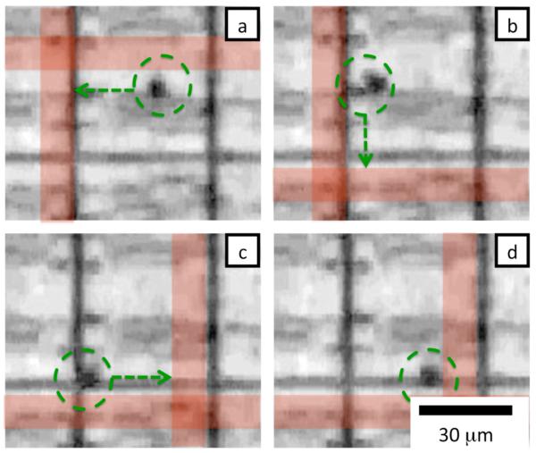
In Fig. 4 the magnetic matrix is used to trap and move iron-oxide beads which have a radius a = 1 μm (Bioclone: FF102) along programmed paths. In Fig. 4a two wires are activated with 120 mA (indicated with red lines), such that the bead is trapped at the field maximum that occurs at the wires’ intersection. In Fig. 4(b-d) different intersecting wires are turned on to move the bead along a path at speeds of 10 μm/s. The ability to trap and move magnetic beads along programmable paths is a useful tool to control the position of objects that cannot be trapped with DEP forces, but that can be tagged with magnetic particles.4,7
Fig. 4.
Time sequence of magnetic trapping and positioning of a magnetic bead. Magnetic wires in the matrix are turned on in sequence to position the bead. The position of the particle is marked with a green circle. The direction that the bead is being pulled is marked with a green arrow. The red lines indicate which magnetic wires in the matrix have been turned on, the actual wires are buried under the DEP pixels and are not visible. Each frame (a-d) is separated by roughly 2 sec.
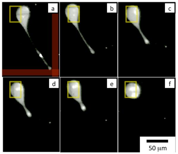
The utility of using MP and DEP forces simultaneously is demonstrated by holding a vesicle in place with DEP while simultaneously stretching a thin tether from its membrane by pulling on implanted iron-oxide nanoparticles with MP.15 The vesicle is positioned with a DEP pixel and two magnetic wires that cross near the DEP pixel are sourced with 120 mA (indicated by red lines in Fig. 5). The vesicle is held in place with DEP body forces as the iron-oxide nanoparticles are pulled towards the magnetic field maximum, as is shown in Fig. 5a. The membrane is locally deformed into a thin tether, as vesicles have been shown to do in the presence of a local force.15 In the proceeding frames Fig. 5(b-f) the magnetic field is turned off and tension in the membrane pulls the tether back into the vesicle.15 The ability to locally deform microscopic objects using the DEP force as a body force and the MP force as a local force is a useful tool to apply precise mechanical stresses on vesicles and living cells.9,10,13
Fig. 5.
A vesicle is held in place with a DEP pixel while a tether is pulled using the magnetic matrix. The yellow square shows the DEP pixel that is activated, and the red lines show the magnetic wires that are turned on. There are iron-oxide nanoparticles suspended in the solution inside the vesicle. After the first frame (a) the magnetic field is turned off and the tether is pulled back into the vesicle. Each frame (a-f) is separated by 0.2 seconds.
IV. Conclusions
Hybrid IC / microfluidic chips provide a versatile platform to programmably control microscopic objects.1-7 The combination of both magnetic4,7 and electric control of microscopic objects,6 onto a single chip further expands the capabilities and generality of the platform. Dielectrophoresis can be used to trap and position untagged living cells and small volumes of fluid packaged in lipid vesicles. Magnetophoresis can be used to trap and to position objects tagged with magnetic nanoparticles that could not be trapped with DEP. Dielectrophoresis and Magnetic forces can be used simultaneously to apply forces to microscopic objects that are held in place with DEP, such as living cells or lipid vesicles.
The combination of DEP and MP on a single chip suggests exciting scientific and technological applications. The technique demonstrated in this paper, pulling a thin tether from a vesicle and observing the tension in the lipid bilayer membrane pull the tether back into itself, is a useful tool to study the mechanical properties of these complex mechanical objects.15 The hybrid IC / microfluidic chip enables many such experiments to be carried out in parallel, enabling high-throughput screening of the mechanical properties of lipid bilayer vesicles. The same technique can also be used for studying living cells that have been tagged with functionalized magnetic nanoparticles.10,11 The capabilities of hybrid IC / microfluidic chips demonstrated in this paper provide important building blocks for a versatile platform that can perform a wide range of biological and chemical applications.12,13
Acknowledgments
We would like to acknowledge generous support from the Harvard-MIT Center for Cancer Nanotechnology Excellence (CCNE) and the Department of Defense (DoD) through the National Defense Science & Engineering Graduate Fellowship (NDSEG) Program. We would also like to thank Donhee Ham and his group at Harvard for their helpful advice and assistance in the design of our integrated circuit.
Contributor Information
David Issadore, School of Engineering of Applied Sciences at Harvard University, Cambridge, MA 02138.
Thomas Franke, University of Augsburg in Germany.
Keith A. Brown, School of Engineering of Applied Sciences at Harvard University, Cambridge, MA 02138
Thomas P. Hunt, Sunprint Inc.
Robert M. Westervelt, School of Engineering of Applied Sciences at Harvard University, Cambridge, MA 02138, westervelt@seas.harvard.edu
References
- [1].Lee H, Ham D, Westervelt RM, editors. CMOS Biotechnology. Springer; New York: 2007. and references therein. [Google Scholar]
- [2].DeBusschere BD, Kovacs GTA. Biosensors & Bioelectronics. 2001;16:543. doi: 10.1016/s0956-5663(01)00168-3. [DOI] [PubMed] [Google Scholar]
- [3].Cui X, Lee LM, Heng X, Zhong W, Sternberg PW, Psaltis D, Yang C. Proc Natl Acad Sci. 2008;105:10670. doi: 10.1073/pnas.0804612105. [DOI] [PMC free article] [PubMed] [Google Scholar]
- [4].Lee H, Liu Y, Westervelt RM, Ham D. IEEE J. Solid-State Circuits. 2006;41:1471. [Google Scholar]
- [5].Manaresi N, Romani A, Medoro G, Altomare L, Leonardi A, Tartagni M, Guerrieri R. IEEE J. Solid-State Circuits. 2003;38:2297. [Google Scholar]
- [6].Hunt TP, Issadore D, Westervelt RM. Lab Chip. 2008;8:81. doi: 10.1039/b710928h. [DOI] [PubMed] [Google Scholar]
- [7].Lee H, Purdon AM, Chu V, Westervelt RM. Nano Lett. 2004;4:995. [Google Scholar]
- [8].Whitesides GM, Ostuni E, Takayama S, Jiang X, Ingber D. Annual Review of Biomedical Engineering. 2001;3:335. doi: 10.1146/annurev.bioeng.3.1.335. and references therein. [DOI] [PubMed] [Google Scholar]
- [9].Chin CD, Linder V, Sia SK. Lab Chip. 2007;7:41. doi: 10.1039/b611455e. [DOI] [PubMed] [Google Scholar]
- [10].Berry C, Curtis ASG. J. Phys. D. 2003;36:198. [Google Scholar]
- [11].Dobson J. Nature Nanotechnology. 2008;3:139. doi: 10.1038/nnano.2008.39. [DOI] [PubMed] [Google Scholar]
- [12].Chiu DT, Wilson CF, Ryttsén F, Strömberg A, Farre C, Karlsson A, Nordholm S, Gaggar A, Modi BP, Moscho A, Garza-López RA, Orwar O, Zare RN. Science. 1999;283:5409. doi: 10.1126/science.283.5409.1892. [DOI] [PubMed] [Google Scholar]
- [13].Tresset G, Iliescu C. Appl. Phys. Lett. 2007;90:173901. [Google Scholar]
- [14].Angelova MI, Dimitrov DS. Faraday Discuss. Chem. Soc. 1986;81:303. [Google Scholar]
- [15].Waugh RE, Song J, Svetina S, Zeks B. Biophysical Journal. 1992;61:974. doi: 10.1016/S0006-3495(92)81904-5. [DOI] [PMC free article] [PubMed] [Google Scholar]


