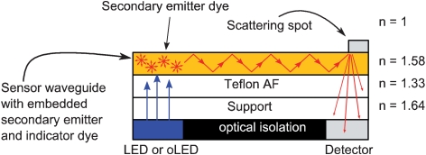
 The novel optical sensor concept utilizes the sensing layer as light propagating layer and employs a new method to couple light into a planar waveguide.
Abstract
An optical sensor concept utilizing the sensing layer as the light propagating layer and a new method to couple light into a planar waveguide is presented. The concept enables simple manufacturing by coating or printing techniques and the integration of organic (plastic) opto-electronic components.
Integrated optical sensors have attracted rapidly growing interest in the last decade. Various integrated optical sensor types have been described including interferometric, refractrometric, reflectometric, fluorescent or absorbance based sensors.1–3 Light is coupled most commonly employing prism coupling, grating coupling or end-fire coupling. The choice of technique employed is a tradeoff between fabrication costs, practicality, and sensor performance.4 A prerequisite of integrated optical sensor for mass applications is cost effectiveness and therefore simple manufacturing processes are required.
In this report we present an optical sensor concept utilizing the sensing layer as the light propagating layer5 and a new method to couple light into a planar waveguide which enables simple manufacturing by coating or printing techniques and the integration of organic (plastic) opto-electronic components.6–8 By analogy to solar concentrators for photovoltaics9,10 we employ a luminescent dye dispersed in the planar waveguide. Light of an external light source is absorbed and re-emitted into the waveguide. The sensing function is introduced into the waveguide by an additionally dispersed indicator dye that absorbs propagating light.
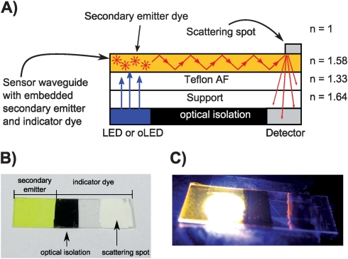
The sensor assembly is shown in Fig. 1. Light is coupled into the sensor waveguide employing a secondary light source which is a luminescent dye embedded into the waveguide layer. The dye is excited by a light source (primary emitter) and emits light isotropically. The fraction emitted in an angle larger than the total reflection angle propagates through the sensing layer is scattered by a so-called scattering spot in a distance of 5–10 mm and is quantified by a detector. An additional indicator dye embedded in the sensor waveguide layer reveals the presence of the analyte by changing its absorption properties.5 Consequently, the intensity of the detected light depends on the amount of guided light that is absorbed by the indicator dye and relates to the amount of the analyte. Excitation and/or emission light guided in the substrate is absorbed by an optical isolation layer. Fig. 1A illustrates the propagation of emitted light in the waveguide layer.
Fig. 1. (A) Schematic side view of the optical sensor utilizing the sensitive layer as the waveguide (not to scale). (B) Top view photograph of the functional sensor waveguide consisting of the secondary emitter zone (yellow), the analyte-sensitive zone with the immobilized indicator and the scattering spot (white). The optical isolation layer is deposited on the backside. (C) The sensor waveguide illuminated with a 460 nm LED. The overexposed white spot results from the LED light. The orange zone results from the emitted light guided and scattered at the scattering spot.
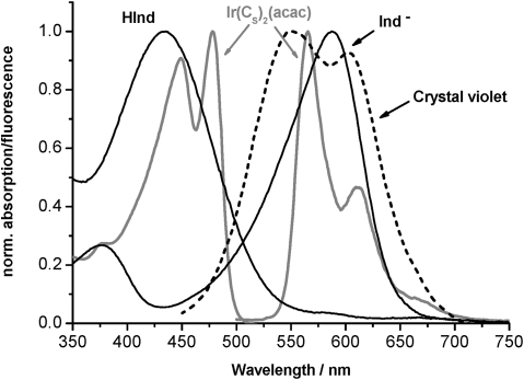
The secondary emitter dye is a key element in the sensor concept and enables light coupling into the sensor waveguide without using gratings or prisms. The excitation light is absorbed in the short optical distance of a few micrometers. Therefore, the secondary emitter dye has to posses a high molar absorption coefficient and good solubility in the host polymer to absorb as much excitation light as possible. Note that high dye concentrations (>1% w/w) commonly result in self-quenching due to aggregation or precipitation of the dye molecules.11 In order to achieve a high coupling efficiency, the secondary emitter dye should posses a high quantum yield to obtain a maximum of re-emitted light, and non-overlapping excitation and emission spectra (large Stokes shift) to avoid a re-absorption of the emitted light by other dye molecules (inner filter effect). This would hamper wave-guiding in the sensor layer. On the other hand the secondary emitter acts as an internal filter for the guided excitation light. The metal ligand complex Ir(CS)2(acac) is ideally suited since it shows an absorption coefficient of 92 800 M–1 cm–1, a quantum yield of 0.54, a large Stokes shift of 93 nm, and sharp emission bands.12 Note that this dye was originally used as an oxygen indicator in optical sensors and therefore shows a cross-sensitivity to oxygen. However, this is not investigated in this proof of principle study. In addition, this dye can be dissolved in host polymers at up to 20 mmol kg–1 (2.5% w/w) without aggregation and luminescence self-quenching. The spectral properties of Ir(CS)2(acac) are shown in Fig. 2. Polymer layers in a thickness of 5 µm doped with 2% w/w Ir(CS)2(acac) showed an absorption of 0.7 at 450 nm (measured in the transmission mode).
Fig. 2. Normalized absorption and emission spectra of the secondary emitter Ir(CS)2(acac) (gray solid). Normalized absorption spectra of crystal violet (black dashed) and the basic and acidic form of m-cresol purple (black solid) employed in the carbon dioxide sensor. Crystal violet (used for distance-dependent measurements) and basic m-cresol purple (Ind–) show good spectral overlap with the emission of the secondary emitter dye resulting in strong absorption of the guided light. On exposure of the sensor to carbon dioxide the basic band disappears, while the acidic band appears and leads to decreased absorption of the guided light.
The sensor is prepared by knife coating and is composed of four layers: a polymeric support with a refractive index of n = 1.64, a low refractive index layer with n = 1.33, a sensing layer with n = 1.50–1.60 (depending on the polymer matrix), and the cover layer (air or water) with n = 1 or n = 1.33. The low refractive index layer below the sensor layer is necessary to achieve wave-guiding in the sensor layer. The thicknesses for the low refractive index layer and the sensing layer are 5 and 1–5 µm, respectively. The size of waveguide sensor is approx. 8–20 mm.
Teflon® AF was chosen for the low refractive index layer because of its outstanding low refractive index of n = 1.33 and the excellent processability on the polymeric support. Additionally, it is solely soluble in per-fluorinated solvents. As a consequence, layers prepared from polymer dissolved in non-fluorinated solvents will not disturb the low refractive index layer. However, Teflon AF shows a high hydrophobicity limiting the range of processable polymer sensor matrices due to de-wetting, disruption and poor adhesion of the sensor layer. This problem was solved by introducing polar groups by oxygen plasma treatment yielding a homogenous coating and adhesion of the sensor layer.
A scattering layer, directly covering the waveguide layer in a region opposite the detector, is used to scatter the guided light to the detector. The layer is composed of TiO2 embedded in a polymer matrix. The light is scattered diffusely by the TiO2 and is quantified orthogonally to the plane of the waveguide by a detector. Approximately one third of the light guided in the waveguide layer is uncoupled through the bottom face due to the high refractive index of TiO2 (n = 2.7 for pure TiO2). The uncoupling efficiency through the bottom face of the sensor device (opposite the TiO2 scattering spot) was measured with an integrating sphere. An optical isolation material composed of black paint is used to absorb excitation light and the light emitted by the secondary emitter dye guided in the polymeric support.
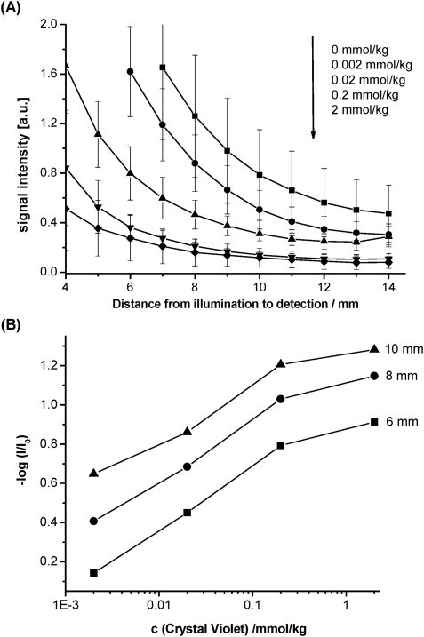
The proof of principle is demonstrated by embedding an inert absorption dye showing a good spectral overlap with the secondary emitter dye. Crystal violet is employed in varying concentrations together with the metal–ligand complex in a fixed concentration in a (poly)styrene matrix. This mimics a sensor response of increasing or decreasing absorption properties of the indicator dye in dependence of an analyte. The different sensors were excited with an LED and the scattered guided light was collected with an optical fibre and guided to a detector (PMT) in varying distances. Excitation light guided and not absorbed by the optical isolation layer was blocked with a long pass filter (λ > 590 nm). The intensity of the detected light depends on the distance of the light source from the scattering spot and the concentration of crystal violet as shown in Fig. 3A. The distance-dependent decrease in intensity can be explained by the spherical radiation profile of the secondary emitter dye and losses due to the roughness and scratches in the waveguide layer. Fig. 3B clearly reveals that an increase of the concentration of crystal violet yields a higher absorption of guided light travelling through the sensor waveguide. As a consequence, a lesser amount of light reaches the detector.
Fig. 3. (A) Plot of signal intensity vs. distance of illumination and detection for incorporated crystal violet (absorption dye) at concentrations 0, 0.002, 0.02, 0.2 and 2 mmol/kg (from top to bottom). Error bars were calculated from measurements of at least three waveguides. (B) Plot of –log(I/I 0) vs. the concentration of crystal violet at 6, 8 and 10 mm distances from illumination and detection defined as the distance between the LED and the scattering spot. I is the signal for sensor waveguide containing crystal violet and I 0 the signal for the sensing layer without crystal violet.
The concept was applied to a carbon dioxide sensor. The sensing scheme is based on a pH-indicator dye (Ind–, m-cresol purple) and a lipophilic base (B+, tetraoctylammonium chloride) incorporated in a hydrophilic polymer (ethyl cellulose).13 The sensor waveguide layer consisted of two zones containing either the secondary emitter dye or the indicator dye (see Fig. 1B). There is an overlap of ∼1 mm of the two zones. This arrangement was chosen because the lipophilic base is quenching the luminescence of the secondary emitter dye, when employed in one layer. The simplified sensing reaction can be described as follows:
| CO2 + H2O + Ind–B+ ⇌ HInd + HCO3–B+ | 1 |
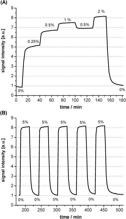
Since the absorption spectra of the basic form of the pH-indicator (Ind–) overlap with the emission of the secondary emitter the intensity of guided light is reduced and a low signal is recorded (Fig. 2B). In the presence of carbon dioxide the pH-indicator is protonated and the absorption in the red part of the spectrum is decreased. Consequently, the amount of guided light hitting the detector is increased. Response curves for various carbon dioxide concentrations are shown in Fig. 4. A total signal change of 800% is observed. The signal drift of approx. 10% in the absence and 1.1% in the presence of carbon dioxide over 7.5 h is attributed to the bleaching of the indicator dye.
Fig. 4. Response curve (A), relative signal change and reversibility (B) of a sensor waveguide exposed to various concentrations of carbon dioxide in nitrogen obtained with a gas mixing device.
In conclusion, we have demonstrated a novel type of integrated optical sensor concept and a method to couple light into a planar waveguide without using prisms or gratings. The entire sensor can be fabricated by solution processing methods using simple coating, inkjet or screen-printing techniques. Existing optical sensor schemes of reagent-mediated optical sensors can be transferred to monitor, for example, pH, ammonia or ions. Herein the extended optical path of 5–10 mm (compared to conventional optical sensor spots of 1–10 µm) is beneficial because the concentration of embedded indicator can be reduced. This results in lower response times for trace analyte sensors, e.g. ammonia. The sensor geometry can be employed for surface plasmon resonance as the sensing principle by depositing a gold layer on the waveguide layer.14
In general, the sensor concept is suitable for application in integrated sensors using established inorganic opto-electronic components. Moreover, it is perfectly suited for a new generation of integrated optical sensors employing organic (plastic) LEDs or photodiodes which can be also processed from solution by printing techniques enabling easy monolithic integration on the sensor itself. This will enable mass production of cheap sensors for a manifold of applications including, for example, environmental analytics, facility surveillance, bio-medical sensors, and point-of-care diagnostics among others.
A key advantage of the described sensor geometry is the simple realisation of sensors arrays: various sensor layers are illuminated by a common organic LED in the centre and are read-out by individual organic photodiodes in a distance of 5–10 mm.
Financial support by the Austrian Science Fund in the framework of the Austrian Nano Initiative (Research Project Cluster 0700 – Integrated Organic Sensor and Optoelectronics Technologies – Research Project Nos. 0701 and 0702) is gratefully acknowledged.
References
- Lambeck P. V. Meas. Sci. Technol. 2006;17:R93–R116. [Google Scholar]
- Gauglitz G. Anal. Bioanal. Chem. 2005;381:141–155. doi: 10.1007/s00216-004-2895-4. [DOI] [PubMed] [Google Scholar]
- Fan X., White I., Shopova S., Zhu H., Suter J., Sun Y. Anal. Chim. Acta. 2008;620:8–26. doi: 10.1016/j.aca.2008.05.022. [DOI] [PMC free article] [PubMed] [Google Scholar]
- McDonagh C., Burke C., MacCraith B. Chem. Rev. 2008;108:400–422. doi: 10.1021/cr068102g. [DOI] [PubMed] [Google Scholar]
- Hisamoto H., Kyung-Ho K., Manabe Y., Sasaki K., Minamitani H., Suzuki K. Anal. Chim. Acta. 1997;342:31–39. [Google Scholar]
- Pieler R., Fureder E., Sonnleitner M. Proc. SPIE. 2007;6739:673919-8. [Google Scholar]
- Shinar J., Shinar R. J. Phys. D: Appl. Phys. 2008;41:133001. [Google Scholar]
- Koetse M., Rensing P., Sharpe R., Van Heck G., Allard B., Meulendijks N., Kruijt P., Tijdink M., De Zwart R., Houben R., Enting E., Van Veen S., Schoo H. Proc. SPIE. 2007;6739:67391D. [Google Scholar]
- Weber W., Lambe J. Appl. Optics. 1976;15:2299–2300. doi: 10.1364/AO.15.002299. [DOI] [PubMed] [Google Scholar]
- Goetzberger A., Greube W. Applied Physics. 1977;14:123–139. [Google Scholar]
- Lee M., Yen C., Yang W., Chen H., Liao C., Tsai C., Chen C. Organic Letters. 2004;6:1241–1244. doi: 10.1021/ol049903d. [DOI] [PubMed] [Google Scholar]
- Borisov S., Klimant I. Anal. Chem. 2007;79:7501–7509. doi: 10.1021/ac0710836. [DOI] [PubMed] [Google Scholar]
- Schröder C., Klimant I. Sens. Actuators, B. 2005;107:572–579. [Google Scholar]
- Ctyroky J., Homola J., Lambeck P., Musa S., Hoekstra H., Harris R., Wilkinson J., Usievich B., Lyndin N. Sens. Actuators, B. 1999;54:66–73. [Google Scholar]


