Abstract
Nanowire field-effect transistors (NW-FETs) have been shown to be powerful building blocks for nanoscale bioelectronic interfaces with cells and tissue due to their excellent sensitivity and their capability to form strongly coupled interfaces with cell membranes. Graphene has also been shown to be an attractive building block for nanoscale electronic devices, although little is known about its interfaces with cells and tissue. Here we report the first studies of graphene field effect transistors (Gra-FETs) as well as combined Gra- and NW-FETs interfaced to electrogenic cells. Gra-FET conductance signals recorded from spontaneously beating embryonic chicken cardiomyocytes yield well-defined extracellular signals with signal-to-noise ratio routinely >4. The conductance signal amplitude was tuned by varying the Gra-FET working region through changes in water gate potential, Vwg. Signals recorded from cardiomyocytes for different Vwg result in constant calibrated extracellular voltage, indicating a robust graphene/cell interface. Significantly, variations in Vwg across the Dirac point demonstrate the expected signal polarity flip, thus allowing, for the first time, both n- and p-type recording to be achieved from the same Gra-FET simply by offsetting Vwg. In addition, comparisons of peak-to-peak recorded signal widths made as a function of Gra-FET device sizes and versus NW-FETs allowed an assessment of relative resolution in extracellular recording. Specifically, peak-to-peak widths increased with the area of Gra-FET devices, indicating an averaged signal from different points across the outer membrane of the beating cells. One-dimensional silicon NW- FETs incorporated side by side with the two-dimensional Gra-FET devices further highlighted limits in both temporal resolution and multiplexed measurements from the same cell for the different types of devices. The distinct and complementary capabilities of Gra- and NW-FETs could open up unique opportunities in the field of bioelectronics in the future.
Bioelectronic interfaces created with nanomaterials represents an exciting and growing field of research that exploits key nanomaterial properties to go well beyond the capabilities of conventional microfabricated electronics.1–8 For example, several groups have recently reported electrical measurements from cells and tissue interfaced to NW-FETs, with results demonstrating high signal-to-noise recording from cultured neurons, muscle cells, embryonic chicken hearts and acute brain slices.4–8 Unique features of these studies compared to conventional planar devices measurements, include (i) the exceptional small active area of the NW-FET devices and (ii) the fact that nanodevices protrude from the plane of the substrate. The former feature enables high spatial resolution, while the latter can increase device/cell interfacial coupling. Indeed, studies have shown that nanostructured interfaces can enhance cellular adhesion and activity,9–14 and thus it is likely that NWs and other nanomaterials may have an intrinsic advantage for building interfaces to cells and tissue.
In this latter regard another interesting nanomaterial that bridges between one-dimensional NWs and conventional planar electronics is graphene, which consists of a single atomic layer of sp2-bonded carbon atoms.15–16 The fundamental physical properties of graphene electronic devices have been investigated extensively,15–16 although relatively little is known about interfacing graphene with biomaterials.17–19 Because the two dimensional structure of the graphene devices differs significantly, in terms of active detection area and surface topography or roughness, versus one-dimensional NW-FETs it is of substantial interest to investigate and compare cellular interfaces of Gra-FETs to evaluate the prospects of graphene devices for providing any unique capabilities for bioelectronic interfaces. Herein we report the first studies of the conductance signals recorded by Gra-FETs as well as combined Gra- and silicon NW-FETs interfaced to spontaneously beating embryonic chicken cardiomyocytes.
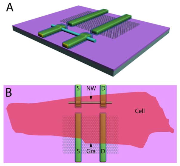
The overall design of our experiments is illustrated in Figure 1. First, the basic nanoFET device chips (Figure 1A) consisted of Gra- and silicon NW (SiNW) FET devices fabricated using methods described previously.3,20–23 Briefly, single layer graphene flakes were transferred to the surface of an oxidized Si substrate using mechanical exfoliation, source/drain contacts were then defined by electron beam lithography (EBL) followed by Cr/Au/Cr metallization, and then the contacts were passivated using SiO2.23 SiNW-FETs were defined close to Gra-FET devices in a second round of fabrication. Specifically, 30 nm diameter p-type SiNWs were deposited from ethanol solution onto the chip with Gra-FET devices, and then EBL and metallization steps were carried out to define source/drain electrodes.23 Last, the substrate chip was coated with a poly(methyl methacrylate) passivation layer, and 50 μm × 50 μm windows were defined to expose the Gra- and NW-FET devices.23
Figure 1.
Overview of the experimental design. (A) Schematic illustrating the chip design incorporating graphene and SiNW devices, and also highlighting the morphological differences between the graphene and NW devices. (B) Representation of the relative size of cardiomyocyte cell interfaced to typical Gra- and SiNW-FET devices.
Gra- and SiNW-FET device chips were interfaced with embryonic chicken cardiomyocytes as shown schematically in Figure 1B. Nanodevice-cardiomyocyte interfaces were made a flexible manner using our recently reported scheme:7 First, embryonic chicken cardiomyocytes were cultured under optimized conditions on thin polydimethylsiloxane (PDMS) sheets;36 second, a PDMS/cardiomyocyte substrate was transferred into a well, which contains extracellular medium, over the Gra-FET and SiNW-FET chip; third, the PDMS/cardiomyocyte cell substrates was positioned using a x-y-z manipulator under an optical microscope to bring spontaneously beating cells into direct contact with devices (Figure 1B).
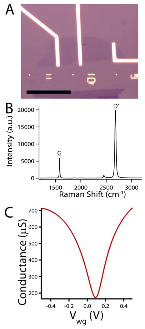
The key features of a representative Gra-FET device are presented in Figure 2. Both optical microscopy (Figure 2A) and Raman spectroscopy (Figure 2B) were used to confirm the layer number of the graphene devices24–26, and show that the Gra-FET in Figure 2A is a single-layer structure. Specifically, the ratio of integrated intensity for the G band (1584 cm−1) and the D′ band (2682 cm−1) in the Raman spectrum is 0.3, matching the value reported from a single layer24. Typical conductance versus back-gate voltage measurements (Figure S1A) show ambipolar behavior with the Dirac point minimum at ca. −7 V. The calculated 2-probe mobility is 4000 and 3550 cm2/V-sec for hole and electron carriers respectively, which is consistent with values for mechanically-exfoliated graphene.27 More importantly, conductance versus water gate (Vwg) data measured in cell medium (Figure 2C) show similar ambipolar behavior with the Dirac point close to Vwg = 0 V. Several key features can be gleaned from the water gate data. (1) The sensitivity of the Gra-FET device can be readily calculated as the slope at a specific Vwg value. (2) The sensitivity can be varied by changing the water gate offset value. (3) The sign of the recorded signal can be inverted while Gra-FET is operated from p- to n-branch. This latter point represents an advantage compared to typical NW-FET devices;3,20–22 for example, representative conductance versus Vwg data for a SiNW-FET used in this study (Figure S1B) shows p-type behavior with the device turned off in the same voltage regime that the Gra-FET exhibits n-type behavior.
Figure 2. Graphene device fabrication and characterization.

(A) optical image of a single layer graphene FET, scale bar is 30μm. The interference contrast is consistent with a single graphene layer. (B) Corresponding Raman spectrum of the graphene device in panel A. (C) Water gate response of a typical Gra-FET.
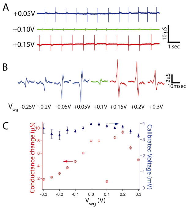
Measurement of the conductance versus time from a Gra-FET in contact with a spontaneously beating cardiomyocyte cell monolayer36–37 (Figure 3A) yields regularly spaced peaks with a frequency of ca. 1.1 Hz and signal-to-noise (S/N), ≥ 4, similar to previously reported signals recorded using SiNW-FETs.5,7 Comparison of the three traces (Figure 3A) also shows that the conductance peak magnitude, which is directly related to the device sensitivity, varies by nearly a factor of 6 with changes in Vwg; that is, data recorded at Vwg = +0.05V, +0.1V and +0.15V had average peak amplitudes of 7.98 ± 0.16, 1.53 ± 0.05 and 8.52 ± 0.12 μS, respectively. Notably, the calibrated voltages for these traces, 3.95 ± 0.08, 3.84 ± 0.12, and 3.71 ± 0.05 mV were the same within experimental uncertainty. These results confirm the stability of the interface between the Gra FET and PDMS/cardiomyocyte cells, and highlight the necessity of recording explicit device sensitivity to interpret corresponding voltages.
Figure 3. Gate effect on Gra-FET recorded signals from cardiomyocytes.
(A) Recorded traces at different applied water gate potentials. The following traces blue, green and red were recorded at +0.05, +0.10 and +0.15 V, respectively. The corresponding sensitivities are 2020, 398, and 2290 μS/V, respectively. (B) Representative expanded peaks for selected gate potentials. Blue resembles traces that were recorded at the p-type polarity of the graphene FET and red peaks represent recorded traces at the n-type device polarity, and green peaks were recorded near the Dirac point of Gra-FET. (C) Summary table of the gate potential effect. Red open circles are the recorded conductance changes average ± 1SD, blue close triangle are the calibrated voltages for each of the corresponding gate potentials (average ± 1SD).
In addition to changes in the conductance peak amplitude as a function of Vwg, careful examination of the recorded data shows that shape or phase of the peaks change. To illustrate clearly the shape of the recorded signals as a function of Vwg, and correspondingly moving from the p- to n-branch of Gra-FET operating regime, we expanded single peaks for representative gate potentials as shown in Figure 3B. These results highlight several key points. First, the signal in both cases shows biphasic characteristics reported previously.7 Second, there is a flip in signal phase when the gate potential changes the Gra-FET from p-type to n-type device characteristics; that is, as Vwg is varied from +0.05 to +0.15 V. These striking changes emphasizing explicitly that recorded signals depend on device sensitivity and are due to a field-effect. We note that the ability to tune the Gra-FET from p-type to n-type device characteristics can provide important confirmation on the nature of recorded signals, which would not necessarily be possible with a unipolar FET.
A summary of the overall quantitative characteristics of the signals versus Vwg from −0.3 to +0.3 V are shown in Figure 3C. The data in Figure 3C can be divided into two segments, where the left corresponds to the p-type Gra-FET regime and the right to the n-type device regime. In the p-type operation mode, the conductance change decreases from 8.0 to 1.9 μS, while in the n-type mode, the conductance change decreases from 8.5 to 5.0 μS. The minimum recorded conductance change, 1.5 μS, occurred close to the Dirac point at Vwg = +0.1 V. Notably, using the measured device sensitivities at each value of Vwg, yields nearly constant calibrated junction voltage of 3.6 ± 0.2 mV (Figure 3C), independent of recording in the p- or n-type device regime or specific Gra-FET sensitivity within either regime.
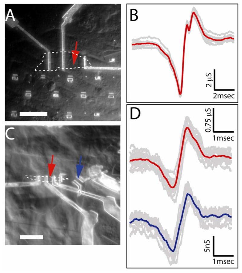
To further investigate the characteristics of Gra-FETs and their potential for recording from cellular interfaces, we investigated the measured signals as a function graphene device sizes and compared these signals to those recorded simultaneously by a SiNW-FET (Figure 4). We first recorded signals using a relatively large Gra-FET with active channel of 20.8 μm × 9.8 μm interfaced to a cardiomyocyte as shown in Figure 4A (device without cell interface, Figure S2A) The recorded conductance versus time data (Figure S3A) exhibited characteristic beating with a frequency of ca. 1.1 Hz. Plotting the individual peaks at high-resolution (Figure 4B) shows that they are quite reproducible with an average (red trace, Figure 4B) peak-to-peak width of 1.31 ± 0.04 msec. In a second case, signals were recorded from a much smaller Gra-FET with active channel dimensions of 2.4 μm × 3.4 μm (Figure 4C and Figure S2B, red arrows). Conductance versus time data recorded using this device showed similar beating behavior (Figure S3B, red curve). Analysis of the peak-to-peak width from the average of the individual peaks (Figure 4D) yielded a value of 0.73 ± 0.04 msec, which is almost a factor of 2 smaller than that obtained from the larger device. In addition, we simultaneously recorded signals from a 0.07 μm2 active area SiNW-FET 16 μm away the smaller Gra-FET (Figure 4C, blue arrow). Analysis of the conductance versus time data for the SiNW-FET (Figure 4D and Figure S3B, blue curves) yields a peak-to-peak width of 0.76 ± 0.04 msec, which is similar to the value for the smaller graphene device.
Figure 4. Size effect on recorded signals.

(A) Optical microscope image of PDMS/cells interfaced with large flake graphene FET. Graphene flake outline is marked by white dashed line, measured device is marked by red arrow. Scale bar is 30μm. (B) Recorded averaged peak (red) and raw data (grey traces) for the Gra-FET and cell in (A). Twelve raw peak signals (gray traces) were aligned in time and then averaged.28 (C) Optical microscope image of PDMS/cells interfaced with smaller flake graphene FET and SiNW FET. Graphene flake outline is marked by white dashed line, measured graphene device is marked by red arrow and measured SiNW device is marked by blue arrow. Scale bar is 13.6 μm. (D) Thirteen raw signal peaks (gray traces) from the Gra-FET (upper data) SiNW-FET (lower data) devices marked by red and blue arrows, respectively, in (C). The peaks were aligned in time28 and the average was plotted in red and blue, respectively.
These results indicate that the signals recorded with the larger graphene device do not represent a localized detection but rather an average of the extracellular potential from sufficiently distinct sources of the beating cell to yield a broadened peak-to-peak signal width. The smaller Gra-FET yielded similar peak-to-peak widths as the ~100× smaller area SiNW-FET, although one-dimensional nanowire devices still have an advantage for spatially-resolved multiplexed measurements in high density device arrays. While it is possible to make ever smaller Gra-FETs, studies indicate that their performance degrades with decreasing size.29–30 Nevertheless, one-atom thick Gra-FETs do demonstrate better performance compared to other planar structures, such as microelectrode arrays (MEAs) and planar FETs,31–35 and do offer the unique capability of recording signals as both p- and n-type devices through simple change of the water gate potential as demonstrated above.
In conclusion, we have demonstrated for the first time recording from eletrogenic cells using single layer graphene devices and have also carried out simultaneous recording using Gra- and SiNW-FETs. Gra-FET conductance signals recorded from spontaneously beating embryonic chicken cardiomyocytes yielded well-defined extracellular signals with signal-to-noise ratio routinely >4, which exceed typical values for other planar devices.31–35 Variations in Vwg showed that the conductance signal amplitude could be tuned nearly an order of magnitude, although the calibrated junction voltages were constant, thus showing a robust graphene/cell interface. Significantly, variations in Vwg across the Dirac point demonstrated the expected signal polarity flip, thus allowing both n- and p-type recording to be achieved with the same device simply by offsetting Vwg. Comparisons of peak-to-peak recorded signal widths made as a function of Gra-FET device size and versus SiNW-FETs showed that the widths increased with the area of Gra-FET devices, indicating an averaged signal from different points across the outer membrane of the beating cells. One-dimensional silicon NW- FETs incorporated side by side with the two-dimensional Gra-FET devices further highlighted limits in both temporal resolution and multiplexed measurements from the same cell for the different types of devices. The distinct and complementary capabilities of Gra- and NW-FETs could open up unique opportunities in the field of bioelectronics in the future.
Supplementary Material
Acknowledgments
We acknowledge helpful discussions and help with figure preparation from B. Tian. Y.F. acknowledges support of this work by Special Presidential Foundation of the Chinese Academy of Sciences, China (08172911ZX) and the National Natural Science Foundation of China (20973045). C.M.L. acknowledges support of this research from a NIH Director’s Pioneer Award (1DP1OD003900) and a National Security Science and Engineering Faculty Fellow (NSSEFF) award (N00244-09-1-0078).
References
- 1.Timko BP, Cohen-Karni T, Qing Q, Tian B, Lieber CM. IEEE Trans Nanotechnol. 2009 doi: 10.1109/TNANO.2009.2031807. [DOI] [PMC free article] [PubMed] [Google Scholar]
- 2.Kotov NA, Winter JO, Clements IP, Jan E, Timko BP, Campidelli S, Pathak S, Mazzatenta A, Lieber CM, Prato M, Bellamkonda RV, Silva GA, Kam NWS, Patolsky F, Ballerini L. Adv Mater. 2009;21:3970–4004. [Google Scholar]
- 3.Patolsky F, Timko BP, Zheng GF, Lieber CM. MRS Bull. 2007;32:142–149. [Google Scholar]
- 4.Patolsky F, Timko BP, Yu G, Fang Y, Greytak AB, Zheng G, Lieber CM. Science. 2006;313:1100–1104. doi: 10.1126/science.1128640. [DOI] [PubMed] [Google Scholar]
- 5.Timko BP, Cohen-Karni T, Yu G, Qing Q, Tian B, Lieber CM. Nano Lett. 2009;9:914–918. doi: 10.1021/nl900096z. [DOI] [PMC free article] [PubMed] [Google Scholar]
- 6.(a) Pui T-S, Agarwal A, Ye F, Balasubramanian N, Chen P. Small. 2009;5:208–212. doi: 10.1002/smll.200800919. [DOI] [PubMed] [Google Scholar]; (b) Eschermann JF, Stockmann R, Hueske M, Vu XT, Ingebrandt S, Offenhäusser A. Appl Phys Lett. 2009;95:083703-1–083703-3. [Google Scholar]
- 7.Cohen-Karni T, Timko BP, Weiss LE, Lieber CM. Proc Natl Acad Sci USA. 2009;106:7309–7313. doi: 10.1073/pnas.0902752106. [DOI] [PMC free article] [PubMed] [Google Scholar]
- 8.Qing Q, Pal SK, Tian B, Duan X, Timko BP, Cohen-Karni T, Murthy VN, Lieber CM. Proc Natl Acad Sci USA. 2010 doi: 10.1073/pnas.0914737107. [DOI] [PMC free article] [PubMed] [Google Scholar]
- 9.Cellot G, Cilia E, Cipollone S, Rancic V, Sucapane A, Giordani S, Gambazzi L, Markram H, Grandolfo M, Scaini D, Gelain F, Casalis L, Prato M, Giugliano M, Ballerini L. Nat Nanotech. 2009;4:126–133. doi: 10.1038/nnano.2008.374. [DOI] [PubMed] [Google Scholar]
- 10.Gheith MK, Sinani VA, Wicksted JP, Matts RL, Kotov NA. Adv Mater. 2005;17:2663–2670. [Google Scholar]
- 11.Sniadecki N, Desai RA, Ruiz SA, Chen CS. Ann Biomed Eng. 2006;34:59–74. doi: 10.1007/s10439-005-9006-3. [DOI] [PubMed] [Google Scholar]
- 12.Stevens MM, George JH. Science. 2005;310:1135–1138. doi: 10.1126/science.1106587. [DOI] [PubMed] [Google Scholar]
- 13.Arnold M, Cavalcanti-Adam EA, Glass R, Blümmel J, Eck W, Mantlehner M, Kessler H, Spatz JP. Chem Phys Chem. 2004;5:383–388. doi: 10.1002/cphc.200301014. [DOI] [PubMed] [Google Scholar]
- 14.Park J, Bauer S, von der Mark K, Schmuki P. Nano Lett. 2007;7:1686–1691. doi: 10.1021/nl070678d. [DOI] [PubMed] [Google Scholar]
- 15.Geim AK. Science. 2009;324:1530–1534. doi: 10.1126/science.1158877. [DOI] [PubMed] [Google Scholar]
- 16.Geim AK, Novoselov KS. Nat Mater. 2007;6:183–191. doi: 10.1038/nmat1849. [DOI] [PubMed] [Google Scholar]
- 17.Ohno Y, Maehashi K, Yamashiro Y, Matsumoto K. Nano Lett. 2009;9:3318–3322. doi: 10.1021/nl901596m. [DOI] [PubMed] [Google Scholar]
- 18.Mohanty N, Berry V. Nano Lett. 2008;8:4469–4476. doi: 10.1021/nl802412n. [DOI] [PubMed] [Google Scholar]
- 19.Lu CH, Yang HH, Zhu CL, Chen X, Chen GN. Angew Chem Int Ed. 2009;48:4785–4787. doi: 10.1002/anie.200901479. [DOI] [PubMed] [Google Scholar]
- 20.Zheng G, Patolsky F, Cui Y, Wang WU, Lieber CM. Nat Biotechnol. 2005;23:1294–1301. doi: 10.1038/nbt1138. [DOI] [PubMed] [Google Scholar]
- 21.Patolsky F, Zheng G, Hayden O, Lakadamyali M, Zhuang X, Lieber CM. Proc Natl Acad Sci USA. 2004;101:14017–14022. doi: 10.1073/pnas.0406159101. [DOI] [PMC free article] [PubMed] [Google Scholar]
- 22.Patolsky F, Zheng G, Lieber CM. Nat Protoc. 2006;1:1711–1724. doi: 10.1038/nprot.2006.227. [DOI] [PubMed] [Google Scholar]
- 23.Graphene flakes were deposited by mechanical exfoliation of natural graphite on top of a silicon substrate with either 285 nm or 310 nm SiO2. Single-layers were identified by their contrast under optical microscopy and further confirmed by Raman spectra. To this end, a micro-Raman spectroscopy (Renishaw in Via Raman Spectroscope) was used. The wavelength and the power of the laser were set to 514 nm and 1.0 mW. A 100 × objective lens with N.A.= 0.90 was used to focus the laser beam on the sample and gave a laser spot of about 1.0 μm in diameter. Graphene devices were fabricated by e-beam lithography (EBL) (30 keV), metalized by thermal evaporation of 5 nm Cr/40 nm Au/5 nm Cr and subsequently passivated with 50 nm SiO2 before final lift-off. The 30 nm diameter p-type SiNWs were synthesized as described previously20–22, and transferred to the surface of the oxidized silicon. NWs near the graphene devices were selected, and source/drain electrodes were defined using EBL, metalized by thermal evaporation of 1.5 nm Ti/50 nm Pd/5 nm Ti. Last, the substrate is coated with 300 nm poly(methyl methacrylate) (150 nm PMMA 495 C2, 150 nm PMMA 950 C2, Microchem Corp.) as a passivation layer, and 50μm × 50 μm windows were opened only at the graphene and the SiNW devices by another EBL step (30 keV).
- 24.Graf D, Molitor F, Ensslin K, Stampfer C, Jungen A, Hierold C, Wirtz L. Nano Lett. 2007;7:238–242. doi: 10.1021/nl061702a. [DOI] [PubMed] [Google Scholar]
- 25.Blake P, Hill EW, Castro Neto AH, Novoselov KS, Jiang D, Yang R, Booth TJ, Geim AK. Appl Phys Lett. 2007;91:063124-1–063124-3. [Google Scholar]
- 26.Chen F, Xia J, Tao N. Nano Lett. 2009;9:1621–1625. doi: 10.1021/nl803922m. [DOI] [PubMed] [Google Scholar]
- 27.Novoselov KS, Geim AK, Morozov SV, Jiang D, Zhang Y, Dubonos SV, Grigorieva IV, Firsov AA. Science. 2004;306:666–669. doi: 10.1126/science.1102896. [DOI] [PubMed] [Google Scholar]
- 28.Individual spikes are first extracted from the full trace. The first spike is used as reference and each of the rest of the spikes is aligned with it in time such that the correlation coefficient is maximized between them. All the spikes are then averaged to yield the averaged trace. Multiple averaged traces are obtained from consecutive full recordings to obtain the standard error of the peak-to-peak width.
- 29.Han MY, Ozyilmaz B, Zhang Y, Kim P. Phys Rev Lett. 2007;98:206805-1–206805-4. doi: 10.1103/PhysRevLett.98.206805. [DOI] [PubMed] [Google Scholar]
- 30.Li X, Wang X, Zhang L, Lee S, Dai H. Science. 2008;319:1229–1232. doi: 10.1126/science.1150878. [DOI] [PubMed] [Google Scholar]
- 31.Halbach MD, Egert U, Hescheler J, Banach K. Cell Physiol Biochem. 2003;13:271–284. doi: 10.1159/000074542. [DOI] [PubMed] [Google Scholar]
- 32.Heer F, Hafizovic S, Ugniwenko T, Frey U, Franks W, Perriard E, Perriard JC, Blau A, Ziegler C, Hierlemann A. Biosens Bioelectron. 2007;22:2546–2553. doi: 10.1016/j.bios.2006.10.003. [DOI] [PubMed] [Google Scholar]
- 33.Meyer T, Boven KH, Gunther E, Fejtl M. Drug Safety. 2004;27:763–772. doi: 10.2165/00002018-200427110-00002. [DOI] [PubMed] [Google Scholar]
- 34.Ingebrandt S, Yeung CK, Krause M, Offenhausser A. Biosens Bioelectron. 2001;16:565–570. doi: 10.1016/s0956-5663(01)00170-1. [DOI] [PubMed] [Google Scholar]
- 35.Yeung CK, Ingebrandt S, Krause M, Offenhausser A, Knoll W. J Pharmacol Toxicol Methods. 2001;45:207–214. doi: 10.1016/s1056-8719(01)00150-2. [DOI] [PubMed] [Google Scholar]
- 36.White Leghorn chick embryos (Charles River Labs) were maintained in a humidified incubator (Carolina Biological Supply Company) at 37.5°C, and hearts were isolated from embryos at E10 – E15 stage. Isolated hearts were immediately transferred to a phosphate buffer solution maintained at 37.5°C. The hearts were minced and then digested in collagenase II (Gibco, Inc.) until all the heart tissue disintegrated into cells. The cell suspension was then centrifuged and the supernatant was discarded, the cell pellet was resuspended in 10% FBS DMEM medium and was incubated for 1 h in a 75 mL flask to clean the cell culture as much as possible from fibroblasts. After 1 h the cell suspension was then collected, cells were counted using a standard hemacytometer and were seeded on PDMS thin sections modified with Fibronectin (BD, Biosciences Inc) with concentrations varying between 2.5×10⁵ cells/mL to 2×10⁶ cells/mL. The medium was exchanged with N2 (Invitrogen, Inc.) supplemented DMEM:F12 (ATCC, Inc.) medium after 24 h and then every other day. Cells spontaneously contracted after 1–2 days in culture.
- 37.All studies were carried at 37.5°C using Tyrode solution (Sigma-Aldrich Inc.). An Ag/AgCl wire was used as a reference electrode. The Gra-FET and SiNW-FET conductance was measured with DC bias set to 60 mV using a battery source. The drain current was amplified with a variable gain amplifier (1211 current preamplifier, DL Instruments, Inc.) and filtered using a low pass of 0–3 kHz filter (CyberAmp 380, Molecular Devices). The output signal was recorded at an acquisition rate of 50–100 kHz using a multichannel A/D converter (Digidata 1440A, Molecular Devices) interfaced with a PC running pClamp 10.1 electrophysiology software (Molecular Devices). Post-analysis was completed in Igor Pro (Wavemetrics).
Associated Data
This section collects any data citations, data availability statements, or supplementary materials included in this article.


