Abstract
An optoelectronic microdevice is set up to drive single microparticles and a maximum synchronous velocity (MS-velocity) spectrum method is proposed for quantifying the frequency-dependent behaviors of individual neutral microparticles from 40 kHz to 10 MHz. Dielectrophoretic behaviors of three types of microparticles are investigated under the optically induced nonuniform electric field. Different MS-velocity spectra for the three different particles are experimentally found. Numerical calculations for the MS-velocity spectra of polystyrene microparticles are performed. The spectrum of the MS-velocities for a specific particle is mainly determined by the particle inherent property and the electric characteristics of the device. Moreover the experimental and the numerical MS-velocity spectra are compared to be accordant. Based on the dielectrophoretic (DEP) behaviors of the particles under a nonuniform electric field, microparticles can be finely characterized or distinguished according to their distinct MS-velocity spectra.
INTRODUCTION
Dielectrophoresis1 (DEP) is a phenomenon of the movement of neutral particles induced by nonuniform electric fields. The magnitude and direction of the DEP force acting on a particle depends on the actuated signal frequency. Therefore, microscopic particle behaviors under DEP mechanism often vary with the change in the signal frequency. The frequency-dependent behaviors of particles under DEP mechanism can serve the functions of distinguishment,2 trapping,3, 4 transport,5, 6 separation,7, 8 sorting,9 and focusing10 of micron or submicron sized particles and physiological investigation11 for biological particles.
There are mainly three embodiments of the frequency dependence of the electrically neutral particle response induced by DEP force. The first is the frequency-dependent force or voltage needed to levitate particles against gravity in three dimensional (3D) microstructure;12, 13 the second is frequency-dependent collection rate at which the particles are driven toward or away from microelectrodes;14, 15, 16 the third is the frequency-dependent velocity under traveling-wave DEP (Refs. 17, 18) or electrorotation DEP (Refs. 19, 20) actuated by multichannel sinusoidal voltages with relative phase shifts. However, most of the previous work employed costly microelectrode arrays or 3D microstructures to produce the nonuniform electric fields. In their work, the researched object is the frequency-dependent behaviors of a population of microscopic particles, not a specific single particle, which bring much difficulty to characterize a specific particle of interest.
In this paper, an electrodeless planar device is introduced to investigate the frequency-dependent behaviors of single neutral microscopic particles. In this device, the microparticles can be driven by optical virtual electrode21, 22 and have flexile and complex motion behaviors. Based on the behaviors of those particles under the nonuniform electric fields induced by the optical virtual electrode, a maximum synchronous velocity (MS-velocity) spectrum method is proposed which can be utilized to discriminate and analyze specific single particles. The numerical calculation model for MS-velocity spectrum is also established and the numerical calculations for single particles are performed. Then the experimental and numerical MS-velocity spectra are compared and found to be accordant.
MATERIALS AND DEVICE CONFIGURATION
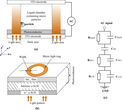
The schematic of the optoelectronic microdevice is shown in Fig. 1. A liquid chamber containing microparticles is sandwiched between a transparent top indium-tin-oxide (ITO) electrode and a lower photoconductor [see Fig. 1a]. A 120 μm insulating spacer is used to maintain the gap between the upper ITO film and lower photoconductor. The upper clamp of the microdevice is an ITO-coated glass slide. The lower clamp of the microdevice consists of a photoconductor and an ITO film electrode fabricated on the glass substrate. The photoconductor was fabricated by PECVD technology and it is composed of a 50 nm n+ hydrogenated amorphous silicon (n+a-Si:H) layer, a 1.5 μm intrinsic a-Si:H photoconductive layer, and a 25 nm silicon carbide (SiCx) passivation layer, as shown in Fig. 1b. The electrical conductivity of a-Si:H without light illumination is about 5×10⁻⁷ S∕m. When the projected light illuminates the a-Si:H layer, its conductivity increases to approximately 0.7 mS∕m. This photosensitive a-Si:H layer allows microlight patterns to control the electric field distribution in the liquid chamber. The relative permittivities of a-Si:H and SiCx layer are 11.68 and 7.5, respectively. The solution in the liquid chamber consists of de-ionized water and small amount of KCl, which has a conductivity of approximately 3.5 μS∕cm. An alternating current (ac) bias was applied across the top and bottom ITO film electrodes. The liquid layer and photoconductor of the microdevice can be equivalent to the parallel structure of resistances and capacitances, as shown in Fig. 1c. “edl” denotes the electrical double layer whose thickness in assumed as 10 nm and “a-Si” indicates the combination layer consisting of intrinsic a-Si:H and n+a-Si:H.
Figure 1.
Schematic of optoelectronic microdevice. (a) The sectional view of the optically induced device. The microlight pattern is projected onto the photoconductor in the directions shown by the vertical arrows. (b) Detailed structure of the photoconductor. The microlight ring is used to trap a single particle via ODEP trap mechanism. (c) Equivalent electric model of the microdevice. Each structural layers of the microdevice can be equivalent to a parallel structure of resistance and capacitance.
PRINCIPLE AND THEORY
Nonuniform electric field in the optoelectronic device
The part of the photoconductor in light area and that in dark area have different electric conductivities when a microlight pattern is projected upward onto the photoconductor, as shown in Figs. 1a, 1b. In dark areas, the majority of the applied voltage is vertically dropped across the photoconductor because the photoconductor impedance is much higher than the liquid impedance, which causes that only a minority of the voltage is across the liquid layer. In contrast, in light areas, the photoconductor impedance is reduced by several orders of magnitude, and most of the voltage is dropped across liquid layer, thus, a high electric field is produced. As a result, a nonuniform electric field profile is created by the light-dark optical patterns and a high field gradient around the boundary between the light and dark areas is formed in the liquid chamber.
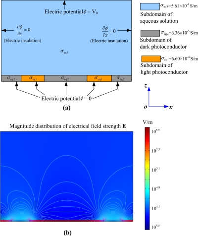
According to the electric model of the microdevice configuration, as shown in Fig. 1c, the impedance of each structural layer varies with the signal frequency because of the capacity effect. So, at each frequency point, there is a corresponding impedance value for each structural layer in this microdevice. To characterize each layer’s electrical property at a certain frequency point, the equivalent conductivity is calculated and employed as an input parameter for the electric field simulation in a commercial finite-element program. If the impedance is denoted as Z(f), then the equivalent conductivity (σeq) of a structural layer can be derived as σeq=t∕[Z(f)S], where t is the thickness of the structural layer and S is area of the structural layer. At the frequency of 100 kHz, the equivalent light conductivity (σeq1) and dark conductivity (σeq2) of the photoconductor were calculated as σeq1=6.60×10⁻⁴ S∕m and σeq2=6.36×10⁻⁵ S∕m, respectively, while the equivalent conductivity of liquid layer (σeq3) were calculated as σeq3=5.61×10⁻⁴ S∕m. Based on the values of σeq1, σeq2, and σeq3, the electric field simulation is performed under the condition that a microlight ring is projected onto the photoconductor (presented in Fig. 1) with a 6 V voltage via a commercial finite-element program (COMSOL MULTIPHYSICS 3.2A, Electromagnetics Module). The objective is to solve the partial differential equation (two-dimensional Laplace equation) that governs the electric potential ϕ in each subdomains shown in Fig. 2a, i.e., [∂2ϕ(x,z)∕∂x2]+[∂2ϕ(x,z)∕∂z2]=0. Then the electric field strength E can be obtained through E=−∇ϕ. Simulation boundaries are presented in Fig. 2a (V0=6 V). The condition at the interface between the water and photoconductor layers is that both the potential and the normal component of the current continue. Simulation result is shown in Fig. 2b, and it is seen that the electric field is nonuniform and largest field strength exits inside the dark photoconductor (a-Si:H). At the bottom half of the liquid chamber, the field strength E around the light photoconductor is much larger than that in other area without light illuminating. This nonuniform distribution of the field inside the liquid chamber is the basis of the following theory.
Figure 2.
The simulation of the distribution of electric field strength inside the microdevice shown in Fig. 1. (a) Boundary conditions for simulating electric field in the microdevice and three different subdomains are set with their respective electric parameters. (b) Distribution of the electric field strength in the microdevice. The difference in log10(E) between any adjacent isolines is 0.02.
MS-velocity of the particle undergoing optically induced DEP
Because the electric field is nonuniform in the liquid chamber of the microdevice [see Fig. 2b], a spherical particle contained in the liquid chamber will undergo a DEP force expressed analytically by1
| (1) |
where R is the particle radius, εm is the solution permittivity, E is the amplitude of electric field including no contributions due to the particle itself,23 and CMF(f) is Clausius–Mossotti factor, which is a function of the field frequency f and indicates the inherent property of the particles and suspension. and are the f-dependent complex permittivities of the particle and suspending medium, respectively. Moreover, and , where σp and σm are Ohmic electrical conductivities of the particle and suspending medium, respectively; εp and εm are the permittivities of the particle and suspending medium. The DEP force generated in the microdevice integrated with photoconductor should be called optically induced DEP (ODEP) force because the nonuniform field is induced by the bright-dark optical pattern on the photoconductor film. The selectively illuminated photoconductor film can thus be described as dynamic “virtual electrodes.” In this kind of ODEP-based device, electro-osmosis should be taken into account only when low-bias frequency (<1 kHz) is applied to the ODEP device.24, 25 In this paper, the operation frequency is always more than 40 kHz so the influence of electro-osmosis (including induced-charge electro-osmotic flow) definitely could be neglected.
Under the action of the ODEP force, the particle will be accelerated and starts to move. Once it moves, an opposing Stokes’ drag force will be produced. This frictional force can be expressed as26
| (2) |
where η is the dynamic viscosity of the liquid, v is the particle velocity, K is the coefficient of correction, and h is the distance from the surface to the particle center. At equilibrium in the direction of the particle linear motion (assumed as x-direction), it should satisfy the following equation: FDEPx+Ff=0, i.e., the particle reaches its stable horizontal traveling velocity. When negative DEP is available (CMF<0), the light pattern will repel the particles away from the light area. If a single particle is circled by a planar optical ring projected onto the photoconductive layer, as shown in Fig. 1, the repulsive DEP force will always horizontally drive the particle to the center of the optical ring. Once the optical ring moves, the particle will follow the motion of the optical ring. In this way, the particles can be transported to a desired position.
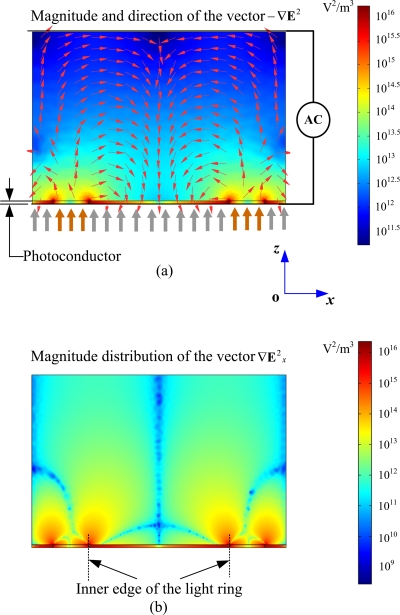
To investigate the ODEP force in the liquid chamber, the vector ∇E2 in the DEP force expression [see Eq. 1] should be calculated first. As shown in Fig. 3, the cross-sectional distribution of the vector −∇E2 and its x-component ∇E2x (horizontal component) were calculated and simulated based on the distribution of electric field strength in Fig. 2b. This simulation result is for the application of 12 Vp.p. (peak to peak ac voltage) at 100 kHz when a microlight ring is projected onto the photoconductor, as presented in Fig. 1. The simulation results show that the largest ∇E2 in the liquid layer exists on the inner edge of the light ring (referring Fig. 3). Within an optical ring in the x-y plane (referring to the coordinate system in Fig. 1), the horizontally repulsive DEP force produced by the optical ring increases with the distance between the particle and the ring center, which has the largest value around the inner edge of the optical ring (see Fig. 3). However, the trapped particle cannot keep up with the light pattern pace when the light pattern moves very fast because each kind of particles has a maximal DEP force within the optical ring according to the formula |FDEP max|=πR3εm Re[CMF(f)]|∇|E2||max. As we know, Stokes’ drag resistance is proportional to the particle velocity. With the increase in the optical ring speed, the equilibrium position of the particles moves from the center to the inner edge within the optical ring to increase the DEP force. When the particle reaches the inner edge of the ring, as shown in Fig. 3b, the particle experiences the largest horizontal DEP force (FDEPx max) because ∇E2x reaches its largest value ∇E2x max at this position, referring to Fig. 3 and Eq. 1. However, when the velocity of the optical ring reaches a certain threshold value, at which even the largest force FDEPx max is not able to overcome the drag resistance, the particle will be lagged behind the optical ring. The threshold value is called as the MS-velocity. At this state, the maximum force value |FDEPx max| equals |Ff|, i.e., FDEPx max+Ff=0, combining Eqs. 1, 2, the particle MS-velocity (maximum horizontal velocity) is obtained as
| (3) |
where ∇E2x indicates the x-component of ∇E2, which is along to the particle horizontal motion direction. From Eq. 3, the MS-velocity vx max can be utilized to characterize the frequency-dependent behaviors of particles since the CMF implies the frequency-dependent property of the particles and suspension. Equation 3 is suitable for clearly illuminating the relationship among the MS-velocity and other physical quantities of particle, solution, and electric field, which is very instructive for independently analyzing each factor influencing the measured MS-velocity spectrum in practical application.
Figure 3.
Distribution of the magnitude and direction of the vector −∇E2. (a)Arrows represent direction of −∇E2 (negative DEP force direction). Surface plot indicates distribution of the magnitude of −∇E2 in x-z cross section of the device projected onto a light ring of 100 μm inner diameter and 25 μm thickness with an actuating signal of 100 kHz and 12 Vp.p.. (b) The magnitude distribution of the horizontal component (x-component) of the vector ∇E2 (denoted as ∇E2x). This calculation is based on the result in (a).
Modified calculation model for MS-velocity of the particle undergoing optically induced DEP
In the above principle explication, the DEP force expression [Eq. 1] based on the point-dipole model of the particle is not very accurate when the radii of particles are comparable to length scale of the nonuniformity of the electric field. Moreover, for more accurate calculation, the distortion of the electric field by presence of the particle should be considered27, 28 in conventional microfluidic device involving no photoconductive effect. However, in this OEDP microdevice, the inaccuracy brought by point-dipole model is still much less than that caused by the other factors influencing the MS-velocity. Specifically, another two more important factors should be considered to modify the basic Eq. 3 for more accurate calculation.
First, the interface distribution capacitance between any two adjoining structural layers or between the ITO pads and electrical wire terminals in the optoelectronic microdevice usually has relative high impedance at the frequencies below 100 kHz, which results in reduction in the bias across the liquid layer and the electric field strength and thus make the particle’s motion slow down. However, these interface distribution capacitances are very difficult to predict and thus not included in the simulation model, as shown in Fig. 2. In this modified calculation model, a quadratic polynomial modified function is employed to reduce the errors caused by interface distribution capacitances.
Second, the attenuation of photoconductivity of a-Si:H layer along the vertical direction (positive z-axis in Fig. 2) also influences the distribution of electric field and |∇E2x|. Moreover, the variation of the photoconductivity along the vertical direction of the thin a-Si:H layer is much difficult to predict accurately and cannot be measured directly for this device. Therefore a correction coefficient should be added into the expression of |∇E2x|max. From the distribution of |∇E2x| (Fig. 3), it follows that the |∇E2x|max exponentially decreases with the height (h) from the chamber bottom when h<60 μm. The value of |∇E2x|max based on the idealized design model of the device can be expressed by |∇E2x|max=α0eβ0h, where α0 and β0 are the parameters depicting the field distribution, which are related to the electric property of the material and structure of the designed device model. In a similar way, the modified value of |∇E2x|max for the actual microdevice in practical application also varies with h exponentially, which can be expressed by (α1≠α0, β1≠β0). Then,
where, β=β1−β0 and κ=α1∕α0. Thus and κeβh is the correction coefficient, which is related to the particle center height h.
Based on the above explication, the modified calculation model for MS-velocity is established as
| (4) |
| (5) |
| (6) |
where P(f) is a modified function that is used to reduce the errors caused by the interface distribution capacitance. fm is the frequency point at which the experimental vx max has the largest value. P(f) equals a quadratic polynomial when f<fm and a constant of 1 when f≥fm. The term of κeβh is the modified coefficient for reducing the error caused by attenuation of photoconductivity along the vertical direction. κ and β are the parameters depicting the variation of field distribution compared to the design model, which can be obtained through the curve fittings. In fact, the P(f) and κeβh meanwhile correct most of the inaccuracy caused by the point-dipole model, which is verified by experimental empiricism.
EXPERIMENTAL CONDITIONS AND OPERATIONS
In our experimental setup, the dynamic white light patterns with certain moving velocities were generated and projected to the photoconductor by a digital micromirror device with a high-pressure mercury lamp as light source and a set of focusing lenses. An actuating ac bias provided by a waveform generator (Tabor Electronics, WW2074) was applied across the top and bottom ITO film electrodes. A charge-coupled device camera (The Imaging Source Europe GmbH, Germany) is connected to the upright microscope (Nikon ECLIPSE 50i) observation port to acquire the particle images through a 10× objective lens (numerical aperture of 0.25) from the top of the optoelectronic device. The dynamic images of particle and light pattern motions were transferred to a monitor.
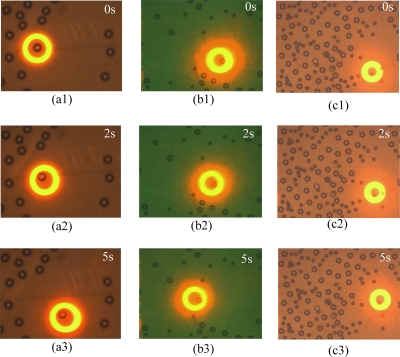
In our test, three types of electrically neutral (uncharged) particles were used, which are ∼19 μm in diameter pollen grains (PGs), 30 μm in diameter polystyrene microspheres (30PMs), and 50 μm in diameter polystyrene microspheres (50PMs) (bought from Duke Scientific Corp.). The surface conductivity (Ks) and bulk conductivity (σbulk) of the polystyrene microspheres (PMs) are 2×10⁻⁹ and 1×10⁻¹⁶ S∕m, respectively, and the relative permittivity (εpr) of PM is ∼2.53. The particles suspended in the solution consisting of de-ionized water and small amount of KCl. Moreover, the solution had a conductivity of 3.5 μS∕cm, which allowed these three types of particles to experience negative DEP. The PG is botanical particle and its structure and inherent property should be characterized by its CMF, which could be derived from its experimental MS-velocity according to the relationship between the CMF and the MS-velocity. Round optical rings are used to trap these three types of particles with the same width of 25 μm (see Figs. 14). The interior diameters of the light rings are 50, 70, and 100 μm for PG, 30PMs, and 50PMs, respectively (see Fig. 4).
Figure 4.
The experimental snapshots of the motions of single particles when the trapping rings were driving the single particles at their MS-velocities approximately with an application of 12 Vp.p. at 200 kHz. (a)(1)–(a)(3) are the test procedures for 50PMs, which is trapped and drove to the bottom right of the screen in a straight path at its MS-velocity. (b)(1)–(b)(3) are the test procedures for 30PMs, which is eccentrically trapped and drove to upper left of the screen in a straight path at its MS-velocity. (c)(1)–(c)(3) are the test procedures for PG, which is eccentrically trapped and drove to the top of the screen in a straight path at its MS-velocity.
The MS-velocity measurement was controlled by optical pattern control software developed by our group (copyright registration No. 2009SR02775 in China), which generates dynamic microlight patterns with certain moving velocities. The motion paths of the optical rings in our experiment are always along straight lines. The initial and final points of the straight path can be arbitrary specified using the optical pattern control software.
RESULTS AND DISCUSSION
Individual particle trapping and driving
Figure 4 illuminates the measuring processes for the three types of particles. The measuring snapshots in Fig. 4 are for the application of 12 Vp.p. at 200 kHz, which demonstrate the typical implement of MS-velocity measurement and are representative for all frequency points. As shown in Fig. 4, the trapped single 50PM moved from the upper left to the bottom right of the observing screen [Fig. 4a(1)–Fig. 4a(3)]; the trapped single 30PM was drove from its initial position to the upper left of the screen in a straight path at its MS-velocity [Fig. 4b(1)–Fig. 4b(3)] and the single PG was drove to the top of the screen in a straight path at its MS-velocity [Fig. 4c(1)–Fig. 4c(3)].
For any driving velocity that is less than the particle’s MS-velocity, the particle will follow its trapping light ring’s motion continuously and thus has the same velocity with the light ring and when the light ring’s velocity changes, the particle’s velocity changes accordingly as long as light ring’s velocity is less than particle’s MS-velocity. Even at the same frequency and voltage, the particle can have many different moving velocities that depend on the driving velocity of the light ring. Nevertheless, the particle has only one MS-velocity at a specific frequency and voltage. So the MS-velocity can be used to characterize the motion response of single particles at a certain frequency point in the optoelectronic device. Further, the MS-velocity spectrum can be used to characterize the frequency response of single particles in the ODEP device.
Experimental MS-velocity spectra of three types of microparticles
The MS-velocity for each particle is measured through the trial and error method. An initial value of the light pattern velocity was set at a certain signal frequency. The velocity is increased slowly until the particles cannot follow up. Once the light pattern velocity causes desynchronization to the particle motion, a fine tune on the velocity is started to determine the exact maximum velocity for the particle at this ac frequency. After the MS-velocity at a certain frequency point was obtained, repeated measuring process was implemented at a new frequency point. The actuating ac bias of 36 Vp.p. is applied in the frequency range from 600 kHz to 10 MHz. For the frequencies ranging from 300 to 500 kHz, the ac bias of 20 Vp.p. is applied, while for the frequency below 300 kHz, the voltage decreased to 12 Vp.p. in order to avoid hydrolysis of the solution.
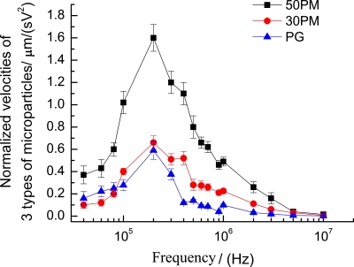
Figure 5 presents the normalized experimental MS-velocity profiles for the three types of particles. It is found that the MS-velocities of the three types of particles significantly vary with the frequency of the applied field. Different particles have different MS-velocity spectrum curves. The three curves all reach their summits at ∼200 kHz, which implies that highly effective manipulation can be realized around 200 kHz for the three particles. Therefore, MS-velocity spectrum can be utilized as a guide for improving the scheme of single particles manipulation. Besides, the MS-velocity spectrum can also be utilized as a guide for filtering or separation of different particles in the same population. For instance, if a light pattern with the driving speed that is smaller than the MS-velocity of 50PMs but larger than those of PG and 30PMs, the 50PMs will be transported to another area while the 30PMs and PG will be left behind. Thus, the 50PMs are able to be filtered out of the mixture of these three particles. So, the optimized strategy for manipulation or separation of particles in ODEP devices should be established in terms of MS-velocity spectrum of particles, which characterizes the frequency-dependent behaviors of particles.
Figure 5.
Normalized MS-velocity profile over the signal frequency range from 40 KHz to 10 MHz for 50PMs, 30PMs, and ∼19 μm ragweed PGs.
The 50PMs always have higher MS-velocity than 30PMs, as shown in Fig. 5, which is mainly due to the larger radius of 50PMs than that of 30PMs according to Eq. 1. However, the ratio of 50PMs’ MS-velocity to 30PMs’ MS-velocity over the measured frequency range for the two particles is not a constant. Specifically, 50PMs’ MS-velocity is ∼3.0–∼3.7 times as large as the 30PMs’ MS-velocity from 40 to 80 kHz, whereas the 50PMs’ MS-velocity is only ∼2.4 times as large as the 30PMs’ MS-velocity from 100 to 300 kHz. Above 400 kHz, the MS-velocity difference between these two particles dramatically decreases versus the frequency. Additionally, the radius of 30PMs is larger than that of PG, but the MS-velocity of 30PMs is smaller than that of PG below 80 kHz, as shown in Fig. 5. Moreover, the ratio of 30PMs’ MS-velocity to PG’s MS-velocity above 80 kHz is not a constant as the case of the 50PMs and 30PMs mentioned above. The reason for that is the influences of the other factors, such as the value of CMF and .
Frequency-dependent value of CMF
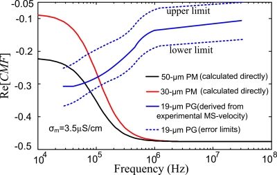
The frequency-dependent behaviors of all microparticles presented in Fig. 5 should be partly attributed to the dielectric property of these particles because the frequency-dependent CMF reflecting the particle property is an essential part of the MS-velocity expression, as given in Eq. 4. As shown in Fig. 6, the CMF curves for the 30PM and 50PM particles are calculated according to Eq. 1 and the parameters of the particle-medium environment stated in Sec. 4. The equivalent conductivity of PMs (σp) can be obtained through the equation29 σp=σbulk+(2Ks∕R). The structure of PG suspending in the liquid is so complex that it is difficult to calculate their CMF directly. Nevertheless, the CMF curve of PG is able to be derived by solving Eq. 4 in terms of the experimental MS-velocity spectrum (detailed parameters could be found in Secs, 5D, 5E). The error limits of the PG CMF are also estimated as shown in Fig. 6.
Figure 6.
Real part of CMF of different particles vs signal frequency. CMF reflects the inherent attribute of the particle-medium system.
Frequency-dependent value of
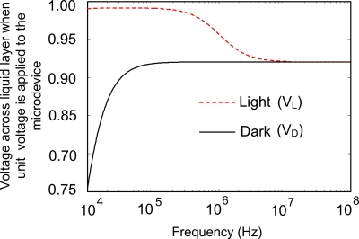
Another factor significantly influencing the frequency-dependent behaviors of microparticles is the frequency-dependent value of at the particle location in the liquid chamber [referring to Eq. 4]. The essential reason for the variation of with the frequency of actuating signal is that the voltages across the liquid layer in light (VL) and in dark (VD) depend on the frequency (see Fig. 7). According to the definition of electric field strength, the magnitude of ∇E2x is directly proportional to (VL2−VD2). The VL and VD are achieved by calculating the impedance of each structural layer of the microdevice and then calculating the voltage across each layer according to the electric model shown in Fig. 1c. As shown in Fig. 7, the frequency-dependent voltages across the liquid layer are approximately constant over the frequencies from 60 to 200 kHz in both light and dark areas. However, above 250 kHz, the light-dark bias difference (VL−VD) across the liquid layer decreases dramatically.
Figure 7.
Theoretically calculated the normalized voltage drop across the liquid layer (the total voltage across the upper and the lower ITO electrodes is set as unit voltage) in the optoelectronic device vs the frequency from 10 kHz to 100 MHz.
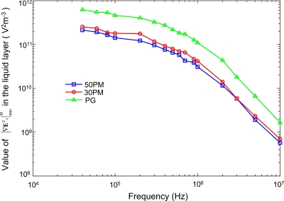
To analyze the MS-velocity spectrum, the value of should be calculated beforehand according to Eq. 4. By using the numerical method presented in Figs. 23 (Sec. 3), |∇E2x|max in Eq. 6 was calculated at each frequency points with an applied voltage of 1 V via the software COMSOL MULTIPHYSICS 3.2A (see Fig. 8). This frequency-dependent value of |∇E2x|max is calculated for the 50PMs, 30PMs, and PG at the spatial locations where the particle levitation heights (distance from particle center to the chamber bottom) are about 30, 20, and 10 μm for 50PMs, 30PMs, and PG, respectively. To make the numerical model fit the experimental results well, the parameters κ and β in Eq. 6 are obtained as 0.118 and 3.74×10⁴ by using the least square method. Then the value of are calculated according to Eq. 6. As shown in Fig. 8, the magnitude of is slightly decreasing from 40 to 200 kHz but dramatically decreases above 300 kHz. Therefore, according to Eq. 3, the increase in the polystyrene particle MS-velocity below 200 kHz can mainly be attributed to the increase in CMF magnitude. On the other hand, the decrease in the particle MS-velocity above 300 kHz should be mainly attributed to the attenuation of with the growing of frequency.
Figure 8.
Values of at the position of the particle geometry center with respect to the frequency of actuating ac signal with an amplitude of 1 V.
Numerical MS-velocity spectra compared to the experimental results
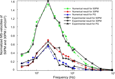
Based on the calculation results of the frequency-dependent physical quantities including CMF and |∇E2x|max, and other essential parameters of standard particles and liquid medium, the numerical calculations are performed according to Eqs. 4, 5, 6. As to the parameters in Eq. 4, K is set as 0.4–0.45 according to the particle heights in the liquid chamber, εm=78.5ε0=6.95×10⁻¹⁰ F∕m and η=1.05×10⁻³ Pa S. The coefficients of the modified function P(f)=af2+bf2+c in Eq. 5 are obtained as a=1.7×10⁻¹⁰, b=1.45×10⁻⁵, and c=0.52 through the polynomial fit method. The comparison between the numerical and experimental results (mean values) is presented in Fig. 9. The numerical MS-velocity spectra are consistent with the experimental results. This comparison verifies the numerical calculation model in Sec. 3. The errors between the numerical and experimental results should mainly stem from the imprecision of device material and structural property, which results in the errors in the performance of electric field calculation. From Fig. 9, the numerical calculation model is able to predict the trend of MS-velocity spectra well, which could be useful for frequency optimization of micromanipulation, discrimination, and characterization of single particles. For instance, we can predict the frequency of 200 kHz as the optimal manipulation and discrimination frequency point because the MS-velocities of 50PMs and 30 PMs both reach the maximum; meanwhile their MS-velocity has the most significant difference at 200 kHz. The numerical MS-velocity spectrum can also used as a reference for designing or improving the ODEP device.
Figure 9.
Comparison between the numerical results and experimental results (mean values) of individual 50PMs, 30PMs, and PG. Numerical MS-velocity spectra were calculated according to Eq. 4.
Comparison of the influences of R, K, Re[CMF], and |∇E2x|max on particles’ MS-velocities
Those behaviors of the 50PMs and 30PMs in this optoelectronic device can be further interpreted and compared via their MS-velocities at the same frequency in Fig. 9. According to Eq. 4, the MS-velocity is proportional to R2, K, Re[CMF], and . The 50PM radius is larger than 30PM radius, meanwhile the Re[CMF] value of 50PMs is also larger than that of 30PMs below ∼1 MHz, as shown in Fig. 6. So it is reasonable that the 50PMs always have higher MS-velocity than 30PMs. Furthermore, the value of K for 50PMs is smaller than 30PMs at the same suspending height according to our calculations. The vertically repulsive DEP force (FvDEP) leads the particle to floating upward against gravity, meanwhile the value of FvDEP is dramatically decreasing with the height growth until the particle arrives at its vertical balance position. The 50PMs undergo larger upward force FvDEP than the 30PM particle due to the larger R and larger Re[CMF] leading to obvious larger DEP force [referring to Eq. 1]. Although 50PMs are under larger downward gravity than 30PMs to counteract the larger upward FvDEP, the 50PMs still have higher height than 30PMs. If the 50PMs and 30PMs both sink to the chamber bottom, the geometric center of 50PMs still has higher height than the 30PMs. The higher height results in the smaller value of |∇E2x|max [Fig. 3b], and consequently, 50PMs always have relatively smaller value of |∇E2x|max than 30PMs. Summarily, 50PMs have larger R and Re[CMF], but smaller K and |∇E2x|max than 30PMs. Also considering the experimental result that the 50PMs always have much larger MS-velocity than 30PMs at all frequency points, therefore, Re[CMF] and R2 reflecting the particle inherent attribute are the main factors determining that the MS-velocities of 50PMs is larger than that of 30PMs at the same frequency point. However, K and |∇E2x|max somewhat counteract the dominated contribution of the larger R and CMF of 50PMs relative to 30PMs.
CONCLUSIONS
In conclusion, an ODEP microdevice is a setup that can be used to trap and manipulate single microparticles. Based on the device, the frequency-dependent behaviors of individual polystyrene and pollen particles measured by the MS-velocity method from 40 kHz to 10 MHz are demonstrated and analyzed. Numerical calculations for MS-velocity spectra are performed through a complete numerical model. The numerical MS-velocity spectra are in accordance with experimental results. The MS-velocity spectrum of each particle is determined mainly by the particle unique dielectric property and the gradient of squared electric field in the microdevice. Further, the differences among the MS-velocities of different particles are mainly determined by the inherent characteristics of those particles. These particles’ MS-velocity spectra contain a wealth of information about the particles, liquid solution, and optoelectronic device. Based on the different spectra of the MS-velocity for different particles, the setup can be used to finely distinguish the microparticles. In addition, it is also helpful to probe the inherent properties of the microenvironments that include colloids or biological particles.
ACKNOWLEDGMENTS
This research work was supported by the National Natural Science Foundation of China (Grant Nos. 50675033 and 30770553) and the National 863 High Technology Program of China (Grant No. 2009AA04Z310).
References
- Morgan H. and Green N. G., AC Electrokinetics: Colloids and Nanoparticles (Research Studies Press, Philadelphia, PA, 2003). [Google Scholar]
- Flanagan L. A., Lu J., Wang L., Marchenko S. A., Jeon N. L., Lee A. P., and Monuki E. S., Stem Cells 26, 656 (2008). 10.1634/stemcells.2007-0810 [DOI] [PubMed] [Google Scholar]
- Hunt T. P. and Westervelt R. M., Biomed. Microdevices 8, 227 (2006). 10.1007/s10544-006-8170-z [DOI] [PubMed] [Google Scholar]
- Kumar S., Seo Y. -K., and Kim G. -H., Appl. Phys. Lett. 94, 153104 (2009). 10.1063/1.3118588 [DOI] [Google Scholar]
- Liu C., Lagae L., and Borghs G., Appl. Phys. Lett. 90, 184109 (2007). 10.1063/1.2736278 [DOI] [Google Scholar]
- Fan D. L., Cammarata R. C., and Chien C. L., Appl. Phys. Lett. 92, 093115 (2008). 10.1063/1.2891091 [DOI] [Google Scholar]
- Iliescu C., Xu G. L., Ong P. L., and Leck K. J., J. Micromech. Microeng. 17, S128 (2007). 10.1088/0960-1317/17/7/S10 [DOI] [Google Scholar]
- Prasad S., Zhang X., Yang M., Ni Y. C., Parpura V., Ozkan C. S., and Ozkan M., J. Neurosci. Methods 135, 79 (2004). 10.1016/j.jneumeth.2003.12.007 [DOI] [PubMed] [Google Scholar]
- Vahey M. D. and Voldman J., Anal. Chem. 80, 3135 (2008). 10.1021/ac7020568 [DOI] [PubMed] [Google Scholar]
- Cheng I. F., Chang H. C., Hou D., and Chang H. C., Biomicrofluidics 1, 021503 (2007). 10.1063/1.2723669 [DOI] [Google Scholar]
- Patel P. and Markx G. H., Enzyme Microb. Technol. 43, 463 (2008). 10.1016/j.enzmictec.2008.09.005 [DOI] [Google Scholar]
- Kaler K. V. I. S., Xie J. -P., Jones T. B., and Paul R., Biophys. J. 63, 58 (1992). 10.1016/S0006-3495(92)81586-2 [DOI] [PMC free article] [PubMed] [Google Scholar]
- Qian L., Scott M., Kaler K. V. I. S., and Paul R., J. Electrost. 55, 65 (2002). 10.1016/S0304-3886(01)00184-X [DOI] [Google Scholar]
- Broche L. M., Labeed F. H., and Hughes M. P., Phys. Med. Biol. 50, 2267 (2005). 10.1088/0031-9155/50/10/006 [DOI] [PubMed] [Google Scholar]
- Fatoyinbo H. O., Hoeftges K. F., and Hughes M. P., Electrophoresis 29, 3 (2008). 10.1002/elps.200700586 [DOI] [PubMed] [Google Scholar]
- Gascoyne P. R. C., Noshari J., Becker F. F., and Pethig R., IEEE Trans. Ind. Appl. 30, 829 (1994). 10.1109/28.297896 [DOI] [Google Scholar]
- Cen E. G., Dalton C., Li Y. L., Adamia S., Pilarski L. M., and Kaler K. V. I. S., J. Microbiol. Methods 58, 387 (2004). 10.1016/j.mimet.2004.05.002 [DOI] [PubMed] [Google Scholar]
- Marczak M. and Diesinger H., J. Appl. Phys. 105, 124511 (2009). 10.1063/1.3152787 [DOI] [Google Scholar]
- Dalton C., Goater A. D., Burt J. P. H., and Smith H. V., J. Appl. Microbiol. 96, 24 (2004). 10.1046/j.1365-2672.2003.02113.x [DOI] [PubMed] [Google Scholar]
- Huang J. P., Yu K. W., Gu G. Q., and Karttunen M., Phys. Rev. E 67, 051405 (2003). 10.1103/PhysRevE.67.051405 [DOI] [PubMed] [Google Scholar]
- Chiou P. Y., Ohta A. T., and Wu M. C., Nature (London) 436, 370 (2005). 10.1038/nature03831 [DOI] [PubMed] [Google Scholar]
- Hwang H., Lee D. -H., Choi W., and Park J. -K., Biomicrofluidics 3, 014103 (2009). 10.1063/1.3086600 [DOI] [PMC free article] [PubMed] [Google Scholar]
- Jones T. B., Electromechanics of Particles (Cambridge University Press, Cambridge, 1995). [Google Scholar]
- Valley J. K., Jamshidi A., Ohta A. T., Hsu H. Y., and Wu M. C., J. Microelectromech. Syst. 17, 342 (2008). 10.1109/JMEMS.2008.916335 [DOI] [PMC free article] [PubMed] [Google Scholar]
- Chiou P. Y., Ohta A. T., Jamshidi A., Hsu H. Y., and Wu M. C., J. Microelectromech. Syst. 17, 525 (2008). 10.1109/JMEMS.2008.916342 [DOI] [PMC free article] [PubMed] [Google Scholar]
- Neale S. L., Mazilu M., Wilson J. I. B., Dholakia K., and Krauss T. F., Opt. Express 15, 12619 (2007). 10.1364/OE.15.012619 [DOI] [PubMed] [Google Scholar]
- Ai Y., Park S., Zhu J., Xuan X., Beskok A., and Qian S., “DC electrokinetic particle transport in an L-shaped microchannel,” Langmuir (in press). [DOI] [PubMed]
- Ai Y., Joo S. W., Jiang Y., Xuan X., and Qian S., Electrophoresis 30, 2499 (2009). 10.1002/elps.200800792 [DOI] [PubMed] [Google Scholar]
- Hughes M. P., Nanoelectromechanics in Engineering and Biology (CRC, Boca Raton, FL, 2003). [Google Scholar]


