

Abstract
There is a need to develop mid-infrared (IR) spectrometers for applications in which the absorbance of only a few vibrational mode (optical) frequencies needs to be recorded; unfortunately, there are limited alternatives for the same. The key requirement is the development of a means to access discretely a small set of spectral positions from the wideband thermal sources commonly used for spectroscopy. We present here the theory, design and practical realization of a new class of filters in the mid-infrared (IR) spectral regions based on using guided mode resonances (GMR) for narrowband optical reflection. A simple, periodic surface-relief configuration is chosen to enable both a spectral response and facile fabrication. A theoretical model based on rigorous coupled wave analysis is developed, incorporating anomalous dispersion of filter materials in the mid-IR spectral region. As a proof-of-principle demonstration, a set of four filters for a spectral region around the C-H stretching mode (2600–3000 cm−1) are fabricated and responses compared to theory. The reflectance spectra were well-predicted by the developed theory and results were found to be sensitive to the angle of incidence and dispersion characteristics of the material. In summary, the work reported here forms the basis for a rational design of filters that can prove useful for IR absorption spectroscopy.
Keywords: Filters, Mid-Infrared, Spectroscopy, Interferometry, Rigorous coupled wave analysis, Guided mode resonance, IR imaging
INTRODUCTION
Mid-infrared (IR) vibrational spectroscopy is one of the most common molecular analysis techniques in use. IR spectral data is almost exclusively acquired using Fourier transform infrared (FT-IR) spectrometers due to their multiplex advantage, ordinate precision, mature instrumentation and versatility.1 A major difference from when FT-IR spectroscopy was being developed and the present day, however, is that IR spectroscopy has been largely supplanted by nuclear magnetic resonance (NMR) spectroscopy to identify molecular structure. Molecular structure verifications today usually consist of comparisons of measured spectra to databases, rather than to first principles elucidation – which is considerably less restrictive than acquiring high-resolution data for fundamental studies. At the same time, advances in instrumentation and their user-friendliness have resulted in the use of IR spectroscopy for fairly routine tasks in process monitoring and quality control. For many of these applications, only a portion of the spectrum is often useful, for example in reaction monitoring, and a low-resolution spectrum is often sufficient for database matching. The use of interferometers for these applications is contraindicated. IR interferometers are exceptionally useful, in contrast, for sophisticated experiments, including imaging,2 circular dichroism3 and perturbation-response4 experiments. Even in these cases, the expense and time required argues against full spectral acquisition as it is often minimally more informative than selected spectral regions5 and certain applications could be faster if smaller volumes of data were acquired, for example, for tissue identification in cancer pathology.6
In FT-IR spectroscopy, large spectral regions are typically acquired. For large regions, the multiplexing advantage for signal-to-noise ratio (SNR) is also accompanied by a disadvantage for noise.7,8 The noise is spectrally uniform while the signal is not; hence, increasing SNR for even a single feature requires substantial effort over the entire spectrum. For characterization of many biological systems, optimal spectral regions and features have recently been identified. 9,10 For example, in a recent application of IR spectral imaging to automated breast pathology, we were able to deduce the appropriate structure of breast tissue and the presence of cancer to high accuracy using only six spectral features.11 By limiting the acquisition to these smaller optimal data sets, the SNR can be increased and acquisition time can be greatly decreased, especially for imaging applications.12 If small spectral regions were acquired, the dynamic range required to detect the signal for a given noise level will also be much lower, allowing for the use of simpler detectors.13 The advantages for acquiring smaller spectral regions and specific feature sets are the primary arguments driving discrete frequency IR (DFIR) spectroscopy,14 in which a small set of spectral features are acquired to characterize the entire spectrum. While it is possible to utilize the conventional grating/slit monochromator and select individual wavelengths for DFIR spectroscopy, light throughput is greatly reduced by the need to spatially restrict the beam and the throughput decreases sharply with aperture size, in turn decreasing the SNR. The recent use of a focal plane array detector for grating based systems15 is very promising but requires an expensive array detector and still measures a large bandwidth. Hence, it is advantageous to explore better and faster approaches to generate narrow-spectral band IR beams. Narrow linewidth, tunable IR quantum cascade lasers16 and nanoscale modified emitters17,18 have been proposed as narrow band sources and can be used for this purpose, but these are expensive and/or span a smaller wavelength range. Similarly, a combination of a fixed bandpass transmission filter and pyroelectric detectors can be used to acquire only one or two measurement wavelengths19. The throughput in such cases is limited and the acquisition rate is suitable where only one or two wavelengths is of interest limiting their application for measuring different spectral bands over a large spectral region. Recently, tunable infrared detectors have been demonstrated using micromachined Fabry-Perot filters20 in 3–5 μm spectral range with bandwidths close to 100 nm, but such devices are limited in the spectral range that could be spanned with a set and their fabrication can be cumbersome and expensive. Hence, technologies that are based on inexpensive components and are easy to deploy with common IR optical elements are still needed.
Here, we propose optical reflection filters based on guided mode resonances (GMR) to provide an inexpensive alternative as a spectral resolution device that can be used with existing optical components in the mid-IR. GMRs are typically observed in substrates with geometrically tailored multilayer thin films of grating and waveguide layers and are a result of coupling diffraction and wave-guiding modes.21 While narrow bandwidth resonant reflection was first experimentally observed as early as 1902,22 recent advances in theory, simulation23 and microfabrication have made large-scale realization of the needed structures feasible. The geometric parameters required to support GMR in the mid-IR spectral region, further, are well within the dimensions of routine contact lithography, making GMR filters (GMRF) feasible for inexpensive, mass production. Several groups have experimentally demonstrated filters based on GMR devices for microwave,24 visible25 and near-IR26,27 regimes. However, GMR optical filters have not been extended to mid-IR as the region represents a unique challenge in terms of fabrication due to strict limits on materials and the extended spectral range. We demonstrate here the first mid-IR GMRFs. In the following sections, we first describe the theoretical framework for GMRF design based on rigorous coupled wave analysis (RCWA). Second, we report a lithography-based fabrication and successful realization of narrow-band reflectance filters. Finally, we compare predicted and recorded responses of filters to validate the production of filters for spectroscopy.
Theory and Modeling
The typical design we propose is depicted in Figure 1 and consists of a soda lime substrate with a thin film of silicon nitride (Si3N4) on its surface. The top part of the silicon nitride film is periodically etched to provide for a grating layer, while the bottom part acts as a wave-guide layer. The introduced periodic modulation allows for phase-matching of an external incident beam into modes that can be re-radiated into free space. These modes possess finite lifetimes and are often referred to as ‘leaky modes’. An incident beam of particular wavelength and orientation undergoes a resonance on coupling to these leaky modes, resulting in high reflection efficiencies. The filter structure critically affects the coupling of incident light. The bandwidth and peak position of the reflected beam spectra can be tuned with parameters of the grating structure, including the grating period (Λ), grating depth (dgr), duty cycle (f) and thickness of the waveguide layer (dwg) depicted in Figure 1. While grating period can be changed relatively easily for a set of GMRFs, depth and thickness of layers are more difficult to change due to the nature of the fabrication process. Hence, we designed structures with different periods while keeping all other parameters constant to allow for simultaneous fabrication of all structures in our validation set.
Figure 1.
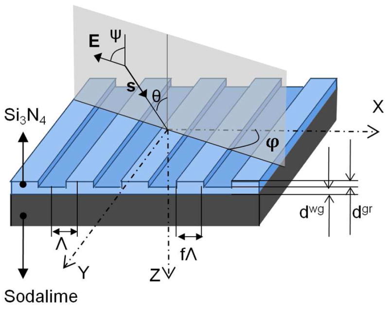
Geometrical configuration and illustration of light incident at a generalized angle to the GMRF.
The incident plane EM wave on the GMR filter structure is diffracted into waves of different orders. The diffraction efficiencies for each order can be exactly evaluated using RCWA. In brief, this method finds solutions to electromagnetic (EM) fields in each of the regions (cover, grating, waveguide and substrate as depicted in Figure 1 that satisfy Maxwell’s equations and invokes the continuity of the tangential components at various interfaces to find their complete description. An efficient and stable implementation of this approach for binary28 and multi-level29 surface relief gratings has already been reported. This method is now well implemented and available in existing commercial software. However, implementation of refractive index dispersion of the material in such software is often not straightforward and hence we have developed an implementation specific to the proposed filter structure. A brief description of our implementation is described below (and in the supplementary information provided).
Coupled Wave Analysis Model
The cover region and substrate region are considered to be semi-infinite and existing in the regimes z < 0 and z > (dgr+dwg) respectively, while the grating layer and wave-guiding layer exist in regimes 0 < z < dgr and dgr < z < (dgr+dwg) respectively. All regions, except for the grating layer, are homogenous in the transverse plane and the grating layer is modulated in the x-direction with a period, Λ, and fill factor, f (fraction filled with a higher refractive index material). The normalized EM field vector of a complex EM wave can be represented in terms of position vector (r), wavenumber (ν) in free space, propagation vector (s) and normalized amplitude vector (A0) as
| (i) |
For an EM wave incident on the GMRF as shown in Figure 1, the propagation direction is at an angle θ relative to the z-axis, ϕ relative to the x-axis and ψ with respect to the plane of incidence. Hence, the incident field can be represented by equation (i) with amplitude function A0 and propagation vector s given by
| (ii) |
In the homogeneous cover region with dielectric constant (εc(v) = [nc(v)+ikc(ν)]2), the propagation components in transverse plane (XY plane) are defined as:
| (iii) |
These relations explicitly describe the coupling of the electrical/optical properties of the material with the electric field of the incident beam. In the mid-IR spectral region, most materials undergo large and, often, anomalous dispersion. Hence, the choice of materials to use is limited both by the desired refractive index and the need to avoid anomalous optical effects. The propagation in z-direction in general can be obtained from the dispersion relation,
| (iv) |
The incident field can be expanded in terms of space-harmonic components in each layer. Each mode of the incident field is diffracted by the presence of modulation in x-direction (in the grating layer). Accordingly the propagation of pth mode in x-direction in the cover region is altered and can be obtained as:
| (v) |
Finally, the diffracted waves in a homogeneous layer  (cover, waveguide and substrate) can be expressed as:
| (vi) |
where the propagation component in z-direction, sz, in each region bounded by (z1 < z < z2) can be obtained by substituting sx′, sy and appropriate dielectric constants in equation (iv). The coefficients Ap and Bp represent the amplitudes of incoming wave from the boundary closer to plane of incidence (z = z1) and incoming wave from the boundary away from the plane of incidence (z = z2) respectively. The magnetic field in the homogeneous layers can also be obtained using Maxwell’s equation as
| (vii) |
where ε0 and μ0 are dielectric constant and magnetic permeability in free space.
To describe the diffracted field in the grating layer, we first need to define its dielectric function εgr. The grating layer has alternate regions of different dielectric properties (ridges and grooves). For simple rectangular ridges and grooves, the periodic relative permittivity (dielectric function) can be conveniently expressed in a Fourier series as:
| (viii) |
where ε1 and ε2 are the refractive indices of the ridges and grooves. Note that tailoring the optical properties of either the ridges or grooves or the difference of both, hence, can also be used to modulate the effective response of the GMRF. The tangential electric and magnetic fields are of particular interest in the grating layer and they can be expanded in harmonic series as:
| (ix) |
The normalized vector amplitude functions M and N can be expressed as functions in position and uncoupled coefficients by relating electric and magnetic fields using Maxwell’s equations, as described in the supplementary information. The expansions given by equation (ix) for the grating layer, equations (vi, vii) for all the other layers and equations (i–iv) for the incident field can be related. Thus the problem simply reduces to solving for the unknown amplitude coefficients (Ap, Bp in equation (vi) and αp and βp defined in supplementary information). Equations governing these quantities can be obtained by applying continuity conditions (as described in the supplementary information).
The diffraction efficiency, DE, for each pth propagating diffracted order is the diffracted power divided by the incident power. With unit incident amplitude, the diffraction efficiency for reflection DEref,p can thus be obtained by using the spatially averaged Poynting vector as follows:
| (x) |
The diffraction efficiency for transmission, DEtran,p can be obtained by substituting coefficients Bc with As in equation (x).
Filter Design
The efficiency of each diffracted order can be calculated using RCWA. However, it is an informative first step to analyze the filter structure as a bi-layer waveguide to find a range of parameters for the eventual GMRF structure. Accordingly, the effective average refractive index of the grating layer to a first order approximation can be written as
| (xi) |
For the surface-relief structure to resemble a waveguide, the refractive indices of grating and waveguide layers have to be such that (nwg, ngr > ns > nc). The materials are chosen to be silicon nitride and soda lime, and a duty cycle f is chosen to be 0.5 for easier fabrication. For the same structure, the reflection resonances are dependent on the polarization state of the incident wave and the angle at which it is incident. With a TE polarized incident wave at angle θ, for a particular order diffracted wave to be a leaky Eigen mode, the introduced modulation parameter should satisfy the inequality30:
| (xii) |
For maximal efficiency, we propose designing filters such that only zero-order propagating waves contribute to the reflected wave while all the higher orders become guided modes (evanescent).
Here, our focus was on fundamental studies involved in validating a framework for GMRFs, rather than a fabrication and use for spectroscopy. Hence, we focused on validations with a small number of filters in the spectral region around the C-H stretching vibrational mode (2600–3000 cm−1). Figure 2A represents the inequality in equation (xii) for the first diffraction orders to be evanescent in this range for different incident angles. The refractive indices are assumed to be real constants for the spectral range listed. At normal incidence, the parameter range overlaps for p = 1 and p = −1 and approximately obeys 1.7 < Λ < 2.7 μm. Larger dimensions are preferred for simpler fabrication; accordingly, we chose 2.2, 2.3, 2.4 and 2.5 μm as Λ values for proposed filter set. The thicknesses of the waveguide and grating layers, subsequently, have to be appropriately chosen to maximize the chosen resonances. Hence, for the selected Λ, we examined different sets of values for dwg and dgr using RCWA to maximize zero order diffraction reflection efficiency. Figure 2B shows the results obtained for normally incident TE polarized wave when dwg = dgr. In these calculations the refractive indices are assumed to be constant and are assigned values listed in the figure. It can be observed that a minimum thickness of 0.3 μm is needed to achieve a reflectance peak in the desired spectral range. We choose the minimum thickness possible to minimize losses due to absorption.
Figure 2.

A) Parameter regimes for Λ, such that |p| = 1 order (on the left, p = 1 and on the right, p = −1) can correspond to a guided mode for 2600 and 3000 cm−1 for TE polarized EM wave incident at angle θ. The dispersion characteristics are ignored and the refractive indices are approximated to be nc = 1.0, nSi3N4 = 2.0 and ns=1. B) The maximum achievable reflectance of structures with chosen Λ values for a TE polarized EM wave that is normally incident. Depth of the waveguide, dwg = dgr and fill fraction, f = 0.5 are arbitrarily chosen for simpler fabrication. The azimuthal angle of incidence is chosen to be ϕ = 0. The dispersion characteristics are ignored and constant real values are chosen for refractive indices as in A).
Experimental Methods: GMRF Fabrication, microscopy and spectroscopic measurements
Filter Fabrication
The filters are fabricated on a 4 inch diameter soda-lime glass wafer using contact photolithography. The sequence of steps involved in fabrication is depicted in Figure 3. Briefly, a 600 nm layer of Si3N4 is deposited onto the substrate by plasma enhanced chemical vapor deposition (PECVD) from a mixture of N2, SiH4 and NH3 flowing at rates of 1960, 80 and 55 cm3/min respectively, all at a pressure of 900 mTorr and temperature of 300 °C. The wafer is then baked at 125 °C for 2 min as a preparatory step to remove any moisture. A photoresist (AZ5214E) is spun coat on the wafer using an adhesion promoter (Hexamethyldisilizane). The adhesive is spun at 4000 rpm for 30 seconds and the photoresist is spun at 5000 rpm for 45 seconds. The wafer is then baked at 110 °C for 50 seconds. The thickness of the photoresist layer obtained is estimated to be 1.25 μm. The wafer surface is then exposed to ultraviolet radiation at 7.5 mW/cm2 for 10 seconds through a chrome mask with the four grating patterns printed on its surface.
Figure 3.

Sequence of steps involved in fabrication of surface-relieved film on soda lime wafer
To reveal the grating pattern, the wafer is then immersed in a developing agent (AZ400 in a 1:4 dilution with water) for 9 seconds. The wafer is then hard baked at 125 °C and then etched by reactive ion etching (RIE) using Freon-14 at 35 mTorr using 90 W. Approximately 490 A° are estimated to be etched in a minute and a grating depth of 300 nm is targeted to be achieved. The wafer is finally cleaned using oxygen plasma treatment, this final de-scum step ensures that the grating layer obtained is smooth.
Analytical Measurements
Microscopy measurements
Atomic force microscopy (AFM) measurements were performed with the probe in AC mode at a frequency of 0.1 Hz with voltage set at 2V. Data were acquired over an area of 5μm×10μm on 512 pixels over 256 scan lines at a 5 μm/s scan rate with no proportional gain and integral gain of 10. The scanning electron microscopy (SEM) images are acquired using a field-emission environmental scanning electron microscope. The structural profiles were obtained from the AFM data by averaging over the 256 scan lines.
Spectroscopic Measurements
The filter responses to a broadband beam from a silicon carbide element source were recorded using an optical setup as shown in Figure 4. An off-axis parabolic mirror is used to collimate the radiation and a wire-grid polarizer was used for polarization. Two parallel circular apertures that restrict the beam to around 10 mm have been employed for filtering out any divergent rays. A beam splitter was employed for measurements of normal incidence case as shown in Figure 4A. The beam splitter and all other optics have been assumed to be of 100 % efficiency. The filter wheel was mounted on a stage with precise control on translation and rotation. It is not possible to achieve a perfectly collimated beam from the extended globar source employed here. Hence, a Zemax model was developed for the optical setup and the half angle divergence is estimated to be ~0.65° due to the multiple apertures and focusing elements. The data was acquired at 4 cm−1 resolution and averaged 16 times. The reflection spectra were evaluated by comparing the filter responses with that of a silver coated substrate. Bruker Vertex 70 spectrometer is used as a detector and the spectra were acquired in the 7000–400 cm−1 spectral region.
Figure 4.

Optical setup for spectroscopic measurements of GMRF for A) normal incidence and B) angular incidence
Results and Discussion
Simulations
Using the parameters for the filter set above in the developed theoretical framework, we simulated reflectance spectra for broadband IR illumination for each of the selected structures as shown in Figure 5A. The four structures of Λ =2.2, 2.3, 2.4 and 2.5 μm possess a maximum reflection efficiency of ~1 at 2987, 2869, 2760 and 2659 cm−1 respectively and distinct bandshapes in the characteristic reflection peak with full width at half-maximum (FWHM) of 50, 42, 36 and 33 cm-1 respectively. Along with these resonance peaks, there exists a much weaker reflection peak due to a higher order guided mode at 5456, 5250, 5063 and 4892 cm−1 respectively.
Figure 5.

A) Reflection spectra (zero-order diffraction efficiency) of the designed filters. The parameters chosen are: Λ = 2.2, 2.3, 2.4 and 2.5 μm, f = 0.5, dgr = dwg = 0.3 μm, nSi3N4 = 2.0, nS = 1.48, nc=1.0. B) E-field distribution in the vicinity of structure with Λ = 2.5 μm at a resonant wavenumber, ν̄= 2659 cm−1 (top) and off-resonance wavenumber, ν̄ = 3400 cm−1. The surface relief of the film to be fabricated is depicted using white lines.
While the higher order modes cannot be avoided, we note that the reflections are substantially weaker and the peak positions are shifted towards the near-IR. While one strategy may be to optimize filter structures such that these peaks are minimized, the ~2500 cm-1 shift from the major reflectance peak implies that bandpass or longpass filters may be used to eliminate their effects. For example, a longpass filter commonly used for undersampling in FT-IR spectroscopy (transmittance of ~0.95% for ν̄< 3950 cm−1) can be used to eliminate the effects of the same. The bandwidths for the structures can potentially be changed (especially, reduced) by considering different values for thicknesses of grating and waveguide layers. Our intention here, however, was to achieve the fabrication of the entire filter set on a single wafer for purposes of comparison with theory. Hence, we choose the same thickness values for grating and waveguide layers.
Finally, the out-of-bandpass or side-band reflections in these filters reach up to 17%. The ratio of the peak reflectivity to the maximum side-band reflectivity can be termed the contrast ratio for the filter. The contrast ratio can be improved, for example, by using additional layers.23 The approach here was to compare theory and fabrication and such methods have not been considered here to keep the fabrication and optical setup simple. To understand the behavior of GMRFs further, we examine one specific case. At peak reflection a lateral standing wave is created inside the filter31, due to the coupling of the two counter-propagating diffracted waves (+1 and −1 orders) which are phase matched to the leaky waveguide mode. The strength of the local electric field in the surface-relieved film can depict the strength of the lateral standing wave setup and the extent to which coupled waves propagate resulting in the multiple interferences of the energy coupled to the waveguide from every grating period. The higher the electric field enhancement inside the surface-relieved film the narrower the far-field resonance is32. In Figure 5B, this standing wave is visualized by the electric field amplitude distribution at a resonant frequency (2659 cm−1) for a filter (Λ = 2.5 μm), which is significantly smaller at an off-resonance frequency (3400 cm−1). Due to the strong modulation for the GMRFs considered here, the maximum electric field enhancement inside the structure is smaller in comparison with enhancements reported in other structures.32
Prior to a comparison with measurements, it is instructive to consider experimental factors that can possibly influence the recorded data and to understand their potential effects using the developed theoretical framework. First, we recognize that spectral reflectance of filters can be significantly altered by differences in the values of refractive indices used in simulation and those that are realized during fabrication.30 Such differences may arise from spectral dispersion, from film structure at the nano-microscale as well as due to confinement effects.33 Second, light in experimental conditions is unlikely to be highly collimated. Hence, the effect of small variations in angles on incidence must be studied. These are two of the largest effects and we examine them next.
The refractive index of silicon nitride in visible region decreases gradually with increasing wavelength. It has a significant dispersion, however, in mid-IR spectral region with intense absorption peaks in the 1400–600 cm−1 spectral range.34 Figure 6A shows the effect on reflectance spectra for one of the structures when dispersion characteristics are considered. When dispersion of the underlying substrate, soda lime,35 is considered, the peak is slightly shifted towards higher wavenumber (from 2869 cm−1 to 2875 cm−1). When dispersion of Si3N4 is considered, the peak shifts towards a lower wavenumber (from 2869 cm−1 to 2853 cm−1) and is of lower efficiency (0.96 in comparison to 1.0). The combined effect of the absorption of Si3N4 layer and surface scattering is a lower peak efficiency (0.95 in comparison to 1.0) and a slight broadening of the reflectance peak (150 cm−1 in comparison to 138 cm−1). The effects due to anomalous dispersion are also apparent in the region below 1600 cm−1. Figure 6B depicts the E-field amplitude distributions considering a constant real refractive index while Figure 6C depicts the E-field distribution when the dispersion characteristics are incorporated into the model. In both cases, a standing wave field is observed indicating the presence of resonances. The local E-field as shown in Figure 6D is only slightly lower for the latter case indicating decreased the slightly broader reflectance peak36. In summary, we note that the refractive index values can influence the position, peak reflectivity and bandshape of the filter. Hence, it is critical to control this parameter during fabrication and operation.
Figure 6.

A) Effect on resonances of dispersion characteristics of Si3N4 and soda lime, for structure of Λ = 2.3 μm, dgr = 0.3 μm, and dwg = 0.3 μm, when a TE-polarized wave is normally incident. B) E-Field amplitude distribution at resonance wavenumber (ν̄ = 2869 cm−1) without considering the dispersion properties of both Si3N4 and soda lime. C) E-field amplitude distribution at resonance wavenumber (ν̄ = 2858 cm−1) considering the dispersion properties of Si3N434 and soda lime.35 The surface relief of the film to be fabricated is depicted using white lines. D) Comparison of E-field amplitude distributions shown in (B) and (C) at the interface of grating and waveguide layers.
The peaks obtained are also strongly coupled to the angle of incidence of the light to be filtered due to the strong modulation in the filter structures. For example, Figure 7 shows the effect of varying incidence angle, θ, on the two reflectance peaks compared to those obtained using normal incidence. Even a 1° variation in θ, results in splitting of the peak at 2858 cm−1 into two peaks at centered at 2880 and 2822 cm−1. The two peaks are slightly different and one of the peaks is broader and shorter. A 5° variation could result in splitting and shifting of peaks by as much as of 140 cm−1. Hence, the optical setup needs to be as precise as possible in measurements and consistently automated when utilizing the filters. At the same time, we note that the peak splitting and shifts can be a facile means to achieve modulation in spectral position. As opposed to amplitude modulation, which may be achieved by a chopper for example, this type of spectral modulation is not possible in interferometry. Hence, the filters present an additional modulation mechanism that remains to be utilized in a smart manner. A trivial application is, of course, in filter alignment such that tilting the filter would bring the peaks closer, eventually resulting in a single reflection peak.
Figure 7.

Spectral variability with changes in incidence angle θ for structure of Λ = 2.3 μm, dgr = 0.3 μm, and dwg = 0.3 μm, when a TE-polarized wave is incident with azimuthal angle ϕ = 0°. Only regions around the two resonances observed in Figure 5 are plotted and significant alterations are observed within both regions. Other spectral regions are insignificantly impacted and hence not shown here.
Filters were fabricated as described in the experimental section. We subsequently characterized the obtained structures using SEM and AFM. While SEM provides a global view of the consistency of fabricated microstructures, AFM provides a quantitative measure of the achieved thickness. From these measurements, we can iteratively refine experimental conditions such that filters with consistently similar structures are obtained. We refined our experimental protocol using several runs and validated that the results are consistent in implementation of the protocol for fabrication. Once routinely consistent filters were obtained, we characterized the measured geometrical parameters with a goal of using them as inputs to the theoretical framework to predict filter response. Results from both modalities of such consistent filters are shown in Figure 8. By averaging over 256 scan lines the values for dgr and Λ are estimated. The standard deviation in the values obtained for dgr is observed to be less than 5 nm while that for Λ is observed to be less than 15 nm.
Figure 8.

(A) Scanning electron microscopy (SEM) image of one of the fabricated GMRFs, and (B) atomic force microscopy (AFM) images of a 1D GMRF, demonstrating the consistency in depth and the periodicity in surface relief.
Structural Parameters
The response of the filter is also very sensitive to the actual geometrical configuration obtained30. The filters fabricated show a good homogeneity of the grating layers as characterized by the structural profile of the grating layers obtained using AFM measurements. Figure 9A shows the average structural profile of the grating layer in the four filter structures offset from each other. The fill fractions can be approximated to be 0.5 from these profiles. The filter responses are relatively insensitive to slight variations in fill fractions and hence an approximate value will suffice. The rectangular profile of the grating grooves cannot be verified from these results, but for convenience we assume straight edges for the groves in calculations. The pitch values derived are close to the targeted values within a ~1% variability. Although the targeted dgr is 0.3 μm, the actual depths obtained were somewhat lower (~0.25 μm). This can be attributed to the etch rate being smaller than that estimated due to a higher SiH4/NH3 flow ratio used in our fabrication process to achieve a Si3N4 film of higher refractive index.37 The thickness of the waveguide layer is obtained using the reflectance measurements at TM-polarized normal incidence.
Figure 9.

A) Structure of the grating layer obtained for the four structures using AFM, (depicted offset from each other here). The AFM results are averaged over 256 scan lines. The structure of the grating layer is used to evaluate Λ and dgr, the standard deviation of dgr is ≤ 0.005 μm and the standard deviation in evaluating Λ is ≤0.015 μm. B) The reflectance efficiencies of the four filters with TM-polarized normal incidence, an appropriate dwg is found with which results predicted by RCWA match those obtained from experiments. C) Structural parameters for the four filters fabricated.
As depicted in Figure 9B, the theoretical predictions and experimental measurements match very well for all the filter structures when a value of 0.4 μm is chosen for dwg. The peaks are relatively broader in the measured data, which is likely due to small angular distribution in the incident beam. The relatively higher base reflectance in the experimental data could be attributed to the background radiation in the optical setup and the scattering at Si3N4-soda lime interface and a finitely thick actual soda lime substrate while the RCWA simulation assumes a semi-infinite medium substrate.38
Validation: comparing predicted and measured spectra
The reflectance spectra of the fabricated filters are measured for TE incidence and are compared with the theoretical predictions. The acquired spectra show distinct peaks in the spectral region of interest as shown in Figure 10. The four structures provide maximal reflection efficiencies of 0.79, 0.74, 0.73 and 0.69 respectively with side bands of peak reflection efficiency of 0.2–0.25. The bandwidths are approximately the same as the design values.
Figure 10.

Comparison of experimentally measured and theoretically calculated reflectance spectra of fabricated GMR filters for a TE-polarized incident wave. The structural parameters are obtained from AFM measurements and reflectance measurements from TM-polarized incidence. These values are listed in Figure 9C.
The H2O and CO2 present in air that permeates the optical setup results in small differences from predicted values around 3800 and 2350 cm−1. The higher baseline for the reflectance exists in TE polarization, as seen for the TM measurements, and can be attributed to the effects due to non-specific reflection at the interface, substrate properties and background response due to optics in the experimental setup. The splitting of the peaks can be modeled better when the responses are calculated by averaging over the variation in angles of incidence (less than or equal to the divergence 0.65° predicted by Zemax models), as illustrated in Figure 11. The match between experimental results and results from simulation is improved but not entirely predicted by the theoretical model we have proposed here. The lack of a perfect match likely implies that a number of other factors, including the variation in azimuthal angle and imperfections in structure and optical properties have to be accurately accounted for a better prediction.
Figure 11.

Comparison of experimental results with theoretical spectra calculated by considering incident beam to have rays varying between θ = 0 to θmax. The θmax values used for structures 1, 2, 3, and 4 respectively are 0.35, 0.35, 0.35 and 0.6° respectively. The integration has been performed using trapezoidal method.
Due to the unavailability of precise refractive index values, the losses due to scattering (at Si3N4 and soda lime interface) and absorption (of bulk material) cannot accurately be accounted for in the simulations. The imperfections in the structure and the deviations from straight edges in grooves and edges have also been excluded from the theoretical model. This, along with the slight variability in the incident beam could be the cause for deviations from ideal predictions. The base reflectance can be eliminated by multiply reflecting off the filters. The experimental measurements at other angles of incidence have also been verified against theoretical predictions and the results have been presented in supplementary information. The unavailability of a collimated IR source is a significant hurdle in rigorously and exactly validating the filter responses. Similarly, the optical setup can be further optimized to yield better efficiencies and lower side-bands. An accurate validation can however only be done by a proper characterization of the incident beam and inclusion of all optical effects in the model.39 Nevertheless, the two major conclusions of the observations and modeling are that, first, fabricated filters possess distinct reflection characteristics with reasonably high efficiencies. Second, reflectance spectra can be understood theoretically. Combined, the two results form a significant first step towards creating appropriate GMRFs for mid-IR measurements. Work is underway40 in optimizing parameters to obtain a desired spectral response from the filters and fabricating the same for use in spectroscopic applications.
Conclusions
Here, GMR reflectance filter structures have been demonstrated for the mid-IR spectral region. We proposed a design based on a surface-relief film of silicon nitride and fabricated structures with distinct characteristics on the same wafer using a lithography approach. While agreement between theory and experiment was generally good, the fabricated filters exhibited slightly lower reflectance and broader bandshapes of the reflectance peak than predicted due to experimental constraints. The simple design and fabrication demonstrated here will allow for mass production while the validation of theory is a first step in creating customized filters of desired reflectance characteristics. Careful design and control of fabricated structures, within the framework of the developed theoretical treatment here, will allow for the production of filters useful for spectroscopic measurements in applications ranging from environmental monitoring of single chemical species to chemical imaging for use in pathology or quality control. We anticipate that the development of routine fabrication of tailored GMRFs and their use will provide problem-driven, targeted spectral data acquisition using inexpensive instrumentation; hence, presenting an attractive alternative to the general-purpose data recording paradigm prevalent today.
Supplementary Material
References
- 1.Griffiths PR, DeHaseth JA. Fourier transform infrared spectrometry. John Wiley & Sons; Hoboken, NJ: 2007. [Google Scholar]
- 2.Lewis EN, Treado PJ, Reeder RC, Story GM, Dowrey AE, Marcott C, Levin IW. Fourier transform spectroscopic imaging using an infrared focal-plane array detector. Anal Chem. 1995;67:3377–3381. doi: 10.1021/ac00115a003. [DOI] [PubMed] [Google Scholar]
- 3.Lipp ED, Zimba CG, Nafie LA. Vibrational circular dichroism in the mid-infrared using Fourier transform spectroscopy. Chem Phys Lett. 1982;90:1–5. [Google Scholar]
- 4.Uhmann W, Becker A, Taran C, Siebert F. Time-resolved FT-IR absorption spectroscopy using a step-scan interferometer. Appl Spectrosc. 1991;45:390–397. [Google Scholar]
- 5.Hamm P, Wiemann S, Zurek M, Zinth W. Highly sensitive multichannel spectrometer for subpicosecond spectroscopy in the midinfrared. Opt Lett. 1994;19:1642–1644. doi: 10.1364/ol.19.001642. [DOI] [PubMed] [Google Scholar]
- 6.Bhargava R. Towards a practical Fourier transform infrared chemical imaging protocol for cancer histopathology. Anal Bioanal Chem. 2007;389:1155–1169. doi: 10.1007/s00216-007-1511-9. [DOI] [PubMed] [Google Scholar]
- 7.Plankey FW, Glenn TH, Hart LP, Wineforder JD. Hadamard spectrometer for ultraviolet-visible spectrometry. Anal Chem. 1974;46:1000–1005. [Google Scholar]
- 8.Voigtman E, Winefordner JD. The multiplex disadvantage and excess low-frequency noise. Appl Spectrosc. 1987;41:1101–1261. [Google Scholar]
- 9.Fernandez DC, Bharagava R, Hewitt SM, Levin IW. Infrared spectroscopic imaging for histopathologic recognition. Nat Biotechnol. 2005;23:469–474. doi: 10.1038/nbt1080. [DOI] [PubMed] [Google Scholar]
- 10.Bhargava R. Towards practical Fourier transform infrared chemical imaging protocol for cancer histopathology. Anal Bioanal Chem. 2007;389:1155–1169. doi: 10.1007/s00216-007-1511-9. [DOI] [PubMed] [Google Scholar]
- 11.Pounder FN, Reddy RK, Bhargava R. Automated diagnoses for human-competetive histologic follow-up to breast cancer screening. Proc Natl Acad Sci. Submitted. [Google Scholar]
- 12.Levin IW, Bhargava R. Fourier transform infrared vibrational spectroscopic imaging: integrating microscopy and molecular recognition. Annu Rev Phys Chem. 2005;56:429–474. doi: 10.1146/annurev.physchem.56.092503.141205. [DOI] [PubMed] [Google Scholar]
- 13.Hoffmann P, Knozinger E. Dynamic range problems in Fourier transform IR and far-IR spectroscopy. Appl Spectrosc. 1987;41:1303–1306. [Google Scholar]
- 14.Kodali AK, Schulmerich M, Cunningham BT, Bhargava R. Discrete frequency infrared imaging for rapid and efficient spectral acquisition. In submission. [Google Scholar]
- 15.Elmore DL, Tsao MW, Frisk S, et al. Design and performance of a planar array infrared spectrograph that operates in the 3400 to 2000 cm(−1) region. Appl Spectrosc. 2002;56:145–149. [Google Scholar]
- 16.Lee BG, Belkin MA, Audet R, MacArthur J, Diehl L, Pflugl C, Capasso F, Oakley DC, Chapman D, Napoleone A. Widely tunable single-mode quantum cascade laser source for mid-infrared spectroscopy. Appl Phys Lett. 2007;91:231101. [Google Scholar]
- 17.Greffet J-J, Carminati R, Joulain K, Mulet J-P, Mainguy S, Chen Y. Coherent emission of light by thermal sources. Letters to Nature. 2002;416:61–64. doi: 10.1038/416061a. [DOI] [PubMed] [Google Scholar]
- 18.Marquier F, Joulain K, Mulet JP, Carminati R, Greffet JJ. Engineering infrared emission properties of silicon in the near-field and far-field. Opt Communications. 2004;237:379–388. [Google Scholar]
- 19.Wilks PA. IR filtometers for today’s analytical measurements. American Laboratory. 1994;26:B42. [Google Scholar]
- 20.Neumann N, Ebermann M, Kurth S, Hiller K. Tunable infrared detector with integrated micromachined Fabry-Perot filter. J Micro/Nanolith, MEMS MEOMS. 2008;7:021004. [Google Scholar]
- 21.Wang SS, Magnusson R. Theory and applications of guided-mode resonance filters. Appl Opt. 1993;32:2606–2613. doi: 10.1364/AO.32.002606. [DOI] [PubMed] [Google Scholar]
- 22.Wood RW. On a remarkable case of uneven distribution of light in a diffraction grating spectrum. Proc Phys Soc London. 1902;18:269–275. [Google Scholar]
- 23.Tibuleac S, Magnusson R. Reflection and transmission guided-mode resonance filters. J Opt Soc Am A. 1997;14:1617–1626. [Google Scholar]
- 24.Magnusson R, Wang SS, Black TD, Sohn A. Resonance properties of dielectric waveguide gratings: theory and experiments at 4–18 GHz. IEEE Transactions on Antennas and Propagation. 1994;42:567–569. [Google Scholar]
- 25.Priambodo PS, Maldonado TA, Magnusson R. Fabrication and characterization of high-quality waveguide-mode resonant optical filters. Appl Phys Lett. 2003;83:3248–3250. [Google Scholar]
- 26.Sharon A, Rosenblatt D, Friesem AA. Resonant grating-waveguide structures for visible and near-infrared radiation. J Opt Soc Am A. 1997;14:2985–2993. [Google Scholar]
- 27.Dobbs DW, Cunningham BT. Optically tunable guided-mode resonance filter. Appl Opt. 2006;45:7286–7293. doi: 10.1364/ao.45.007286. [DOI] [PubMed] [Google Scholar]
- 28.Moharam MG, Grann EB, Pommet DA. Formulation for stable and efficient implementation of the rigorous couple- wave analysis of binary gratings. J Opt Soc Am A. 1995;12:1068–1076. [Google Scholar]
- 29.Moharam MG, Pommet DA, Grann EB. Stable implementation of the rigorous coupled-wave analysis for surface-relief gratings: enhanced transmittance matrix approach. J Opt Soc Am A. 1995;12:1077–1086. [Google Scholar]
- 30.Shin D, Tibuleac S, Maldonado TA, Magnusson R. Thin-film optical filters with diffractive elements and waveguides. SPIE Opt Eng. 1998;37:2634–2646. [Google Scholar]
- 31.Wei C, Liu S, Deng D, Shen J, Shao J, Fan Z. Electric field enhancement in guided-mode resonance filters. Opt Lett. 2006;31:1223–1225. doi: 10.1364/ol.31.001223. [DOI] [PubMed] [Google Scholar]
- 32.Sun T, Ma J, Wang J, Jin Y, He H, Shao J, Fan Z. Electric field distribution in resonant reflection filters under normal incidence. J Opt A: Pure Appl Opt. 2008;10:125003. [Google Scholar]
- 33.Yoon DH, Yoon SG, Kim YT. Refractive index and etched structure of silicon nitride waveguides fabricated by PECVD. Thin Solid films. 2007;515:5004–5007. [Google Scholar]
- 34.Gunde MK, Macek M. Infrared optical constants and dielectric response functions of silicon nitride and oxynitride films. Phys Stat Sol. 2001;183:439–449. [Google Scholar]
- 35.Rubin M. Optical constants and bulk optical properties of soda lime silica glasses for windows. Solar Energy Materials. 1985;12:275–288. [Google Scholar]
- 36.Norton SM, Erdogan T, Morris GM. Coupled-mode theory of resonant-grating filters. J Opt Soc Am A. 1997;14:629–639. [Google Scholar]
- 37.Zhang X, Ding K, Yang A, Shao D. Processing and characterization of PECVD silicon nitride films. Advanced Materials for Optics Electronics. 1996;6:147–150. [Google Scholar]
- 38.Magnusson R, Shin D, Liu ZS. Guided-mode resonance Brewster filter. Opt Lett. 1998;23:612–614. doi: 10.1364/ol.23.000612. [DOI] [PubMed] [Google Scholar]
- 39.Rumpf RC, Johnson EG. Modeling fabrication to accurately place GMR resonances. Opt Express. 2007;15:3452–3464. doi: 10.1364/oe.15.003452. [DOI] [PubMed] [Google Scholar]
- 40.Kodali AK, Schulmerich M, Cunningham BT, Bhargava R. In preparation. [Google Scholar]
Associated Data
This section collects any data citations, data availability statements, or supplementary materials included in this article.