Abstract
This work presents characterization studies of thick silicon double-sided strip detectors for a high-resolution small-animal SPECT. The dimension of these detectors is 60.4 mm × 60.4 mm × 1 mm. There are 1024 strips on each side that give the coordinates of the photon interaction, with each strip processed by a separate ASIC channel. Our measurement shows that intrinsic spatial resolution equivalent to the 59 μm strip pitch is attainable. Good trigger uniformity can be achieved by proper setting of a 4-bit DAC in each ASIC channel to remove trigger threshold variations. This is particularly important for triggering at low energies. The thick silicon DSSD (Double-sided strip detector) shows high potential for small-animal SPECT.
Index Terms: Low energy radiation detectors, silicon DSSD, SPECT
I. Introduction
The field of molecular imaging is experiencing large growth in biological sciences. Among other modalities, nuclear imaging systems such as positron emission tomography (PET) and single photon emission tomography (SPECT) have been reinvented as tools for modern biologists to study the pathways of human diseases in small-animal models. The rapid advances in molecular biology and chemistry will most likely drive the imaging technology forward, manufacturing compact, low-cost imaging systems with high sensitivity, high resolution that provide quantitative images of specific targets in vivo [1]. Making progress in detector and system development for nuclear molecular imaging can be very challenging. In small-animal SPECT theses challenges are largely related to sensitivity due to the use of collimators. Multi-pinhole collimators have found wide application in small-animal SPECT to improve the sensitivity while maintaining a good resolution. A number of novel collimation techniques have been explored [2]-[10] to achieve an optimal trade-off between sensitivity and resolution with multi-pinhole, coded apertures and other type of collimators. These techniques are adapted to the detector characteristics of their SPECT system. In most cases scintillation crystals such as NaI(Tl) and CsI(Tl) are used as either large area detectors [11]-[13] or pixelated detector arrays [14]-[16]. The resolution of these type of detectors has been significantly enhanced by using CCD type of readout sensors coupled to the scintillation material [17]-[19], [32]. Improved intrinsic detector resolution can be accompanied by increased system sensitivity with an optimized the collimator design [20]. The importance of high spatial resolution in SPECT has been a main driving force to develop detectors with even higher resolution. High detector resolution can be traded for sensitivity [35]. In the recent years semiconductor detectors such as CZT [21] or silicon [22], [23] have gained an increased popularity. Unlike PET, SPECT can utilize a larger variety of detectors since its isotopes have a wider range of typically lower energies.
Despite the limited application of silicon-based detectors to low-energy photons, silicon-based SPECT has potential for a wide range of imaging applications with 125I since many important tracers can be labeled with this isotope. We are optimizing a silicon based SPECT system, the SiliSPECT, for some task-specific applications in molecular imaging. One of our proposed applications is imaging mouse brain with tracers that bind to Amyloid Beta (Aβ) plaques, which are considered one of the main pathological hallmarks of Alzheimer's disease. Many Aβ-binding tracers can be labeled with 125I [33], [34]. Typical plaques in mice are between 4μ and 100 μm in size. Due to their heterogeneous and microscopic structure, sub half-mm resolution is required for imaging these plaques and accurately estimating the plaque burden at different stages of Alzheimer's disease. Therefore ultra-high intrinsic detector resolution is of great benefit. The detection efficiency of one millimeter of silicon is expected to be 39% for 125I emissions. Despite its modest detection efficiency, silicon is an ideal material for our proposed type of projection acquisition where two or more detectors are stacked in each camera head. Photons that penetrate through the front detectors without interaction can be detected in the back detectors. The front detectors are expected to contribute 64% of the detected events and the back detectors 36%. The stacked detector configuration also enables the front detectors to acquire projections at a different pinhole magnification than the back detectors. We intend to implement this type of acquisition, using two stationary camera heads. With high detector resolution lower pinhole magnification is required. This together with a smaller number of camera heads allows the design of a more compact SPECT system to scan small objects/organs at very close distances, thus improving the sensitivity. The total system sensitivity also depends on the type of collimators used with these detectors. Using a Monte Carlo simulation in one of our previous studies, we showed that a system sensitivity of 0.083% (830 counts/MBq) can be achieved by using four of these detectors in a dual-headed camera configuration with stacked detector acquisition [29].
In double-sided strip geometry the number of independently processed electronic channels is given by the number of strips (our DSSD: 2048) whereas the number of resolution elements is determined by the number of all strip-pair combinations, which could be significantly larger (our DSSD: 1048576). Double-sided strip detectors have orthogonal strips on each side of the silicon wafer. These strips collect the electron-hole pairs produced as the result of a photon interaction. Therefore, interaction positioning requires a pair of orthogonal strips that make a virtual resolution element. This is a main advantage comparing to pixelated geometry where the individual pixel readout can become a technically limiting factor for achieving higher resolution. The standard silicon DSSDs in industrial manufacturing are usually available in 300 m wafer thickness. While this could to be ideal for tracking charged particles [24] or using these detectors in Compton telescopes [25], implementing these detectors in SPECT imaging systems would require some enhancement in the detection efficiency for gamma rays to improve the total system sensitivity. This can be achieved by increasing the thickness of the silicon wafer. We are proposing a dual-headed, stationary SPECT system that utilizes a new generation of silicon DSSDs with a thickness of one millimeter, an active area of 60.4 mm × 60.4 mm and a new ASIC [30]. We previously demonstrated some preliminary performance characteristics [26] of thick silicon DSSDs.
II. System Description
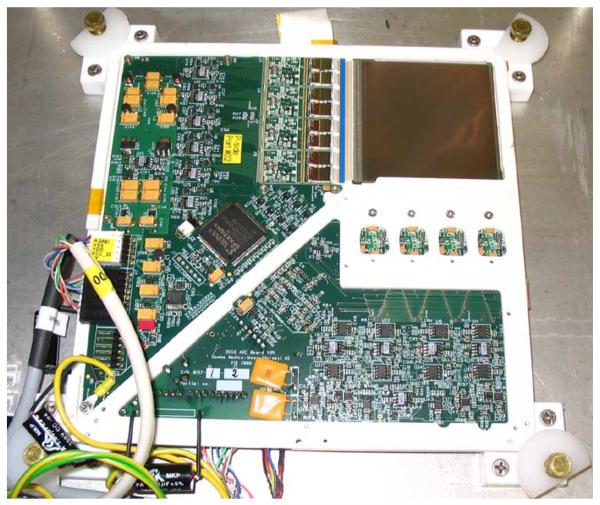
The detector board is shown in Fig. 1. There are 1024 strips on each detector side. The strips on the junction side (P) are orthogonal to the ohmic side (N). The coordinates of the photon interaction are given by the orthogonal pair of strips with the largest induced signal. The detector fabrication was done by SINTEF (The Foundation for Scientific and Industrial Research at the Norwegian Institute of Technology) from a 100 mm wafer using standard ion implantation techniques. The DC-coupled detectors include multi-guard rings and p-stop implants on the n-side. The readout of the silicon DSSD is accomplished using a custom-designed 128-channel ASIC, the VaTaGP6, manufactured by Gamma Medica-Ideas. This ASIC is the latest version of the VaTa family [27], which features self-triggering capabilities with sparse readout [30]. It was specifically tailored to offer stable triggering at low energies with enhanced capabilities for making adjustments to individual trigger levels to minimize channel-to-channel threshold variations. Each strip is wire-bonded to a separate ASIC channel. Therefore, the readout requires 8 ASICs on each detector side for a total of 16 ASICs per detector to process the 2048 independent channels.
Fig. 1.
Image of the detector board with silicon DSSD, located on the top right corner of the board, and the readout electronics. The silicon DSSD is 60 mm × 60 mm × 1 mm.
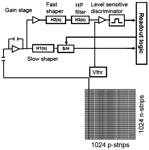
By monitoring this comparatively modest number of channels, we are able to read out 1,048,576 virtual pixels or resolution elements. The ASIC provides each channel with a preamplifier, shaper, sample and hold, fast shaper and comparator circuitry (Fig. 2).
Fig. 2.
Silicon DSSD and front-end electronics scheme.
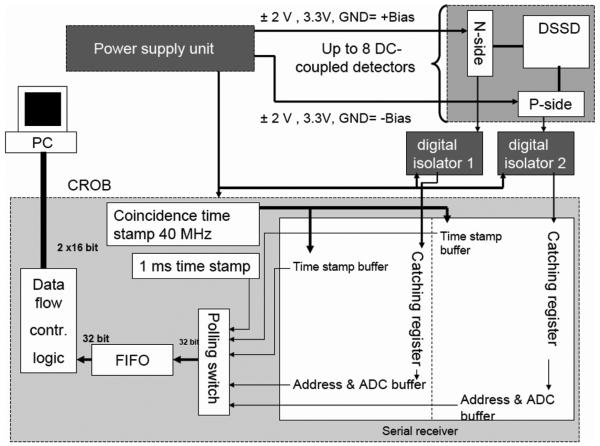
Fig. 3 shows the basic schematic of the data acquisition block diagram. All communication between the front-end and the back-end electronics, the coincidence readout board (CROB), is digital. Since the DC voltages for operating the front-end electronics are referenced with respect to the bias on their corresponding detector side, digital isolators are used to decouple the bias voltage from the signals. Each arriving event is given a time stamp in the CROB based on a 40 MHz clock. This time stamp is referred to as the coincidence time stamp, and is used to determine coincident triggers on the two detector sides. An additional, slower clock writes a time word every millisecond into the event stream, and is used for real-time tracking of count rates. This feature also provides us the option of doing dynamic imaging. The readout system features list-mode acquisition of independently triggered N and P strips for off-line coincidence processing. The events are sent as two 16 bit packets/words from the CROB, and are written to a binary file. By reading back and combining the packet format definitions with bit masking, one can identify and filter out the different packet types in off-line analysis. There are three types of packets (i.e. two 16 bit words) on the data-stream. An event packet indicates the address, ADC value and the module number (detector side) and is always followed by a coincidence packet that indicates the timestamp and module number. An additional time stamp packet is always sent out at a fixed rate. Since the event and coincidence packets come in pairs, the coincident packets are used to identify coincident events. In addition to single channel readout, nearest-neighbor readout is available. The leader event flag in the event packets marks the first, i.e. center channel, in sparse readout. Events from the same module that arrive afterwards without the leader event flag set are neighbors.
Fig. 3.
Block diagram of the data-acquisition system. Up to four detector cards can be supported with a single power supply and CROB.
III. Detector Performance
A. Intrinsic Detector Resolution
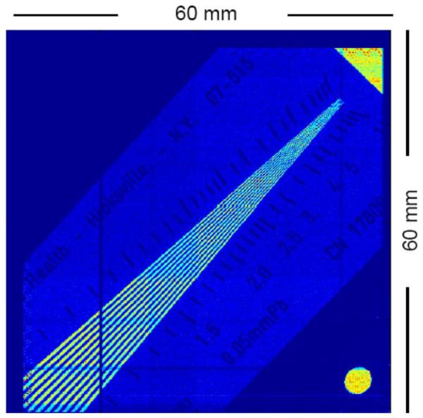
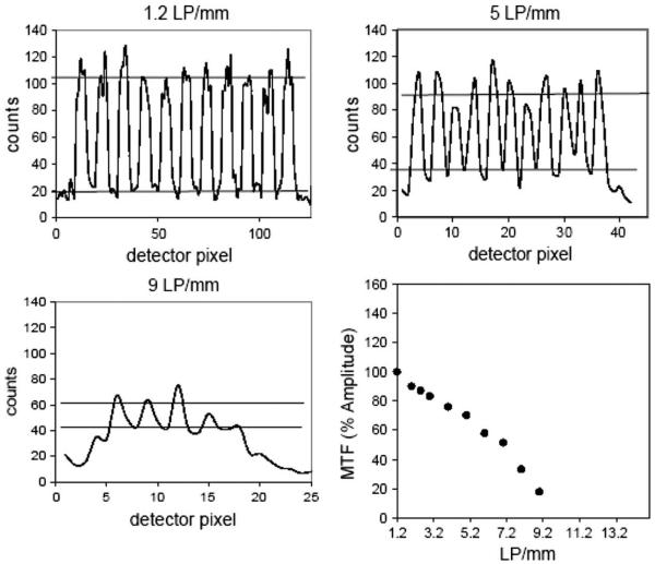
The 59 μm detector strip pitch suggests a high intrinsic resolution. This was measured experimentally by placing a line-pair phantom diagonally on the silicon detector and acquiring the phantom's projection image with a 125I flood source. Line pair (LP) phantoms are commonly used to assess the spatial resolution of x-ray imaging systems. We used the 07-515 model manufactured by Nuclear Associates. The phantom is made of a lead foil and its range of spatial frequency is between 1.0 and 10.0 LP/mm. Fig. 4 shows the projection image of the phantom on the detector. Fig. 5 shows multiple profiles that were taken from the projection image at different spatial frequencies. From these image profiles, we obtained the modulation transfer function (MTF), which dropped to 1/10th of its maximum at 9.5 LP/mm (55 μm).
Fig. 4.
Projection image of the LP phantom on SiliSPECT exposed to 125I flood source.
Fig. 5.
Change of modulation of the phantom image with increasing spatial frequency and the obtained modulation transfer function.
B. Acquisition With Multi-Pinhole Collimator
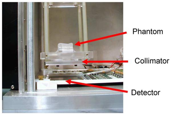
Fig. 6 shows the first experimental setup for the detector acquisition with a multi-pinhole collimator. Both the collimator and phantom were placed in light-tight passively cooled detector box. We used an off-line sorting algorithm to assign coincident events between orthogonal strips. The optimal coincidence timing window was selected based on image analysis methods for this particular acquisition with 63 μCi activity from a pair of 125I brachytherapy seeds (one mm distance) and a multi-pinhole collimator (one mm thickness). The collimator consisted of 127 pinholes, each 250 μm in diameter laser-drilled through the tungsten. The spacing between the pinholes was 2.5 mm. The pinholes were cylindrical in shape and tilted toward a common focal point at a distance of 30 mm away from the collimator surface.
Fig. 6.
Detector acquisition with multi-pinhole collimator and a phantom.
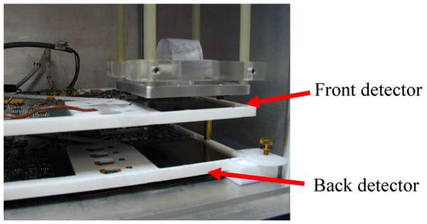
The detection efficiency of a one mm silicon layer is 39% for low energy photons of around 30 keV. This was calculated and verified with Monte Carlo simulations using MCNP5. To offset this moderate efficiency we intend to stack two silicon DSSDs in each camera head [26], increasing the total detection efficiency while at the same time collecting pinhole projection data at two different magnifications. This type of pinhole acquisition is known as synthetic collimation [31], and is an important feature for image reconstruction with limited number of camera heads. We acquired projection data with stacked detectors by adding a second detector below the collimator (Fig. 7). The detectors are mounted in a transmission configuration in such a way that there is no inactive material between them. The distance between the center of the phantom and the collimator was 20 mm. The distance between the front detector and the collimator was 12 mm. The distance between the back detector and the collimator was 32 mm.
Fig. 7.
Experimental acquisition with multi-pinhole collimator, phantom and stacked detectors.
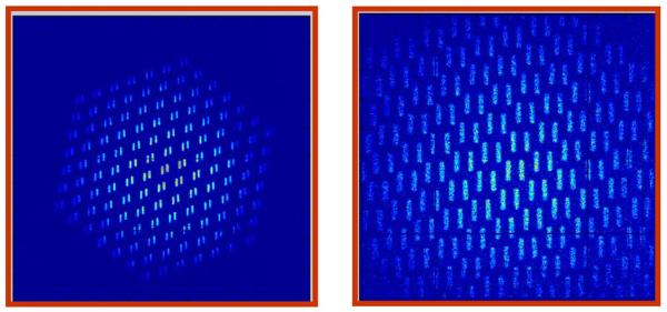
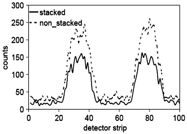
Fig. 8 shows the projection images of the phantom on the front and back detectors. We obtained and compared the profiles of the phantom image on the back detector that were acquired with and without the presence of a front detector (Fig. 9). We compared these profiles with respect to their full width at half maxima and did not detect any significant changes in the profiles in the presence of the front detector other than the expected lower count total due to attenuation of photons in the first detector, indicating the feasibility of using one mm thick silicon detectors in stacked geometry.
Fig. 8.
Experimentally acquired projection images on the front detector (left) and back detector (right) with a multi-pinhole collimator and a pair of line sources as phantom. The pinhole magnification on the front detector is 0.6. The pinhole magnification on the back detector is 1.6.
Fig. 9.
The projection profile of the phantom (2 brachytherapy seeds) on the back detector with and without the front detector present.
C. Timing Properties
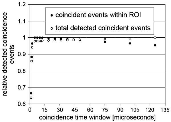
Depending on the trigger count-rate, there is a chance of false coincidence identifications among random strips at large time windows. Random events are mainly associated with noise triggers on one or both of the detector sides. For a given channel, the rate of the noise triggers can increase dramatically, if the threshold of that channel is set too low. These false events contribute to an increased number of total coincident events. However, their positions are randomly distributed across the detector surface, whereas the position of correctly assigned coincident events is determined through the geometry of the multi-pinhole projections on the detector. We implemented image segmentation methods on the projection images generated using different time windows to determine the number of true coincident events within regions of interest (ROI) in the projection image. Fig. 10 shows the relative number of coincident events in the ROI and the total number of identified coincident events across the entire detector surface for different time windows used in the coincidence sorting algorithm. The optimal window was estimated in a timing region where the coincident events within the ROI reached a maximum. This was found to be between 5 and 15 μsec for this particular acquisition.
Fig. 10.
With a multi-pinhole collimator, the position of the true trigger events on the detector is determined by the pinhole geometry. Using image segmentation analysis on the projection data acquired with different time windows in the (off-line) coincidence sorting algorithm, we were able to estimate the increase/decrease of the events that occur out of the region of interest. This gives a possibility to roughly identify the random coincident events because their position is random as well. This method was used to select a time window that minimized the fraction of random events.
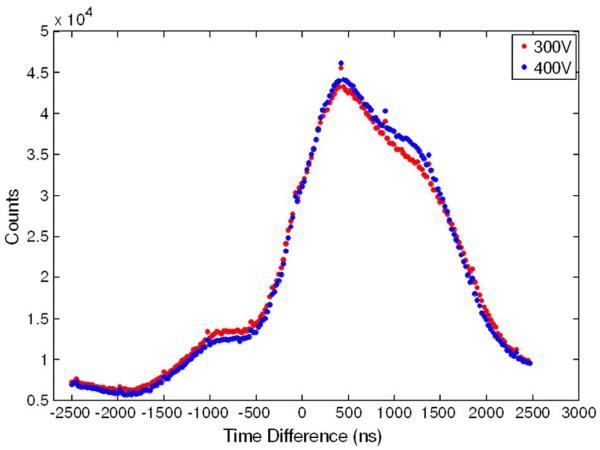
To obtain the coincidence timing spectrum, we collected data from all the detector strips exposed to a 125I source at both 300 V and 400 V detector bias (the depletion voltage is between 90–150 V) and histogrammed their time difference as shown in Fig. 11. A detector bias of 300 V was suggested by the manufacturer. The similarity in the histograms at the two biases indicates that charge-collection time, which depends on the bias voltage, contribute minimally to the timing resolution of this system.
Fig. 11.
Histograms of time differences collected from all detector strips at two different bias voltages.
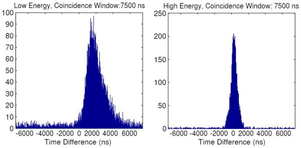
Clinthorne et al. [28] indicated the time-walk resulting from the use of leading-edge threshold along with a fast-shaper peaking time of typically 200–300 ns in the VATAGA device as a possible source of timing degradation in their silicon pad detectors. To estimate the correlation of pulse height versus threshold crossing time difference, we used an Am-241 source and made two separate timing histogram for the low-energy (17 keV x-ray) and high-energy (60 keV) photon emission of Am-241 (Fig. 12). We obtained 500 ns FWHM from the timing difference peak of higher energy photons. The timing histogram of the x-ray photons was significantly degraded in comparison to the higher energy with the asymmetry of the distribution suggesting possible differences between the two detector sides in time-walk effects.
Fig. 12.
Histograms of time differences collected from all detector strips at two different energy windows using an Am-241 source. Using the ADC values, the events (17 keV x-ray) were separated from the high-energy (60 keV) photon emission of the source. A separate timing histogram was created for each group.
Also, the time stamps are generated after the completion of the readout cycle when the digitized signals are transferred to the CROB. This likely contributes to the poor timing resolution seen from the timing histograms since the time-stamping does not follow immediately after the occurrence of the trigger signal. The poor timing resolution could be problematic at higher data frequency, leading to improper association of events from the two detector sides. However, the expected count rates in our SPECT applications (2 kHz) should not be negatively impacted by the timing properties of our detector. We attribute the unusual and non-symmetric shape of the timing histograms to the time differences among different combinations of ASIC pairs. We are investigating the origins of these time differences and ways to correct them.
D. Trigger Uniformity at Low Energy
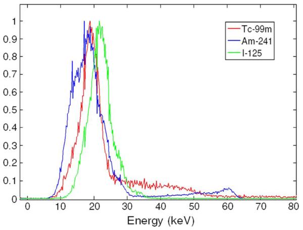
In conventional SPECT imaging, good energy resolution is an important detector characteristic for setting optimal energy windows and suppressing scattered photons. With SiliSPECT, our imaging applications are limited to lower energy photons such as those from the decay of 125I (27.2–35.5 keV). Here, the rejection of Compton scattered photons is not feasible with energy windowing due to the small energy loss even at large scattering angles. The energy threshold should ideally be set just above the noise level to collect photons that interacts in silicon. Fig. 13 shows the energy spectrum of 99 mTc, 241Am, 125I acquired with a single P-side strip. The full width at half maximum of the 18 keV peak of 99 mTC was 5.2 keV.
Fig. 13.
The energy spectra of 99 mTc, 241Am, 125I acquired with a single p-side strip. The full width at half maximum of the 18 keV peak of 99 mTc was 5.2 keV.
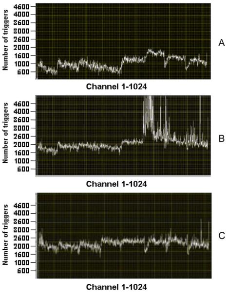
One main requirement for achieving better detection efficiency at low energies without triggering on noise is the capability of adjusting the trigger threshold for individual channels that have different gains and offsets to achieve uniform triggering. For this purpose, the new ASIC has 4-bit DACs associated with each channel for making individual fine adjustments to the main threshold applied to each ASIC. It is important to note that the fast branch of the triggering detection circuit (Fig. 2) determines whether an event has occurred. However, its output is not available to the end user. Therefore, it is necessary to acquire the trigger rate on a channel-by-channel basis as the main threshold level is lowered to determine the level at which the channel triggers on its baseline noise. To achieve uniform trigger rate, the main threshold can be adjusted for each individual channel by modifying the channel's trim DAC. However, this process is not straightforward, mainly due to the generation of offset currents when the channel DACs are modified [36]. Therefore, it is necessary to additionally balance the trim adjustments across the channels to maintain a current-neutral operation condition. This process is performed iteratively. Channels that trigger at significantly different threshold values than the mean over the entire detector side are considered noisy and removed from the subsequent mean calculations. At each iteration, the trim DAC values are updated to shift each active channel's trigger threshold towards the mean value of the results from the previous iteration. This process is continued until trigger thresholds converge. We have developed and implemented software routines that iteratively adjust the channels in a way that the inter-channel variations in trigger response become less than detector acquisitions without the implementation of the channel DACs (Fig. 14). The detector was exposed to a flood source to obtain the trigger histograms A, B and C. Using these histograms we evaluated the trigger uniformity across the strips. In histogram A, the global threshold is set too high so that some channels trigger more than the others due to differences in gain and offset. In histogram B the global threshold is set too low, which causes increased rate of noise triggers for channels with large gains or offsets. For histogram C we achieved more uniform triggering across the detector through individual adjustment of the 4-bit DACs associated with each channel. It is possible to disable noisy strips if needed.
Fig. 14.
Trigger histogram across 1024 channels from one detector side. Nonuniform triggering (a) at high channel threshold without adjusted DACs. Increase of noise triggers (b) at low channel threshold without adjusted DACs. More uniform triggering with less noise triggers (c) at low channel threshold with adjusted channel DACs.
E. Charge Sharing Effects
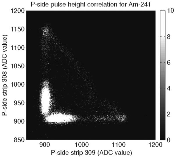
It is important to evaluate the fraction of events where the induced charges in silicon are collected by more than one strip. This charge sharing effect is responsible for the accumulation of events that have lower pulse height in an individual than the actual energy deposited through the photon interaction. It also makes efficient triggering for low energy imaging more difficult due to the increased chances of acquiring noise triggers. It is desired to set thresholds sufficiently low to reliably trigger on events in which not all of the charge is collected on a single strip. For incident photon energies at around 30 keV we intend to set the trigger threshold near 15 keV for an optimal collection of all events. We evaluated the charge sharing effect by including the nearest neighbors in the data readout under flood illumination. Fig. 15 shows the ADC plot of a single strip (channel 309 from P-side) versus a lower neighboring strip (channel 308 from P-side). We used a 241Am source for the data acquisition. Every event was triggered either by channel 309 or channel 308. In 50% of the triggers the produced charges were collected by both the trigger channel and its neighbor.
Fig. 15.
Plot of strip 309 ADC versus lower neighboring strip 308 for Am-241 spectrum. The ~60 keV peak is broadly shared between the strips.
IV. Summary and Discussion
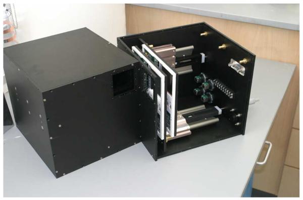
This paper reported some characterization studies of silicon double-sided strip detectors to evaluate their application in low-energy SPECT. The results on the intrinsic detector resolution indicated an excellent resolution matching the detector strip pitch and making these devises suitable for applications that require high spatial resolution such as mouse brain imaging. A global timing window in vicinity of 5 μsec gave the optimal number of correctly assigned coincident events for typical experimental count rates. The poor timing resolution is thought to be influenced by the way the time stamps are generated in the data acquisition process, but should be sufficient for the count rates that we expect to see in our proposed SPECT applications. The energy spectra of individual channels indicate a non-uniform gain and offset across the detector strips, causing pulse height variations. In a detector system with large number of strips (2048), this could have a major impact on our timing resolution. Other studies on one-millimeter silicon pad detectors with VATA ASICs [28] indicated that for a given deposited energy, the depth at which the charge interacts in the detector has a significant influence on the threshold crossing time. Our silicon DSSDs could follow similar behavior. Also our studies on charge sharing effect indicate this effect as another possible source for pulse height variation and its subsequent impact on timing resolution. We will investigate these effects in our future studies. The readout electronics used (VATAGP6) might not be adequate for some imaging applications where very narrow timing window is required to sort the coincident events at higher countrates. However, in our proposed application, SPECT imaging from targeted mouse organs such as brain, the countrate is not expected to exceed 2 kHz, making the current data acquisition system acceptable. The low count rate is mainly given by the modest detection efficiency of silicon and the use of collimators that make the SPECT sensitivity inherently low comparing to other imaging modalities such as PET. For these types of applications, a fast timing window is not mandatory. More importantly, our proposed applications require very high intrinsic detector resolution for imaging small structures with multi-pinhole collimators at low magnification. We made significant improvements in achieving uniform trigger response across a large number of channels at low energies with minimal numbers of noise triggers. With the current ASIC readout we can individually adjust the threshold at each channel using threshold DACs to gain a more uniform triggering across the detector channels. We are optimizing an iterative routine that will adjust the threshold DACs using both the offsets and gain differences among the channels. Using the nearest neighbor readout we looked at the signals where the charges were collected by more than one strip. Our studies on charge sharing effects were limited to a few sample channels, and as part of our future work, we will perform a systematic study on charge sharing. However, from the current results on the measured intrinsic resolution, we can clearly see that the detector resolution does not seem to be degraded by the charge sharing effect. Our detector studies suggest that these types of silicon DSSDs have good potential for our proposed applications using a dual-headed SPECT with stacked detector acquisition. Fig. 16 shows the image of our dual-headed and stationary SPECT camera based on these detectors that is currently under construction.
Fig. 16.
SiliSPECT is a dual-headed SPECT with two silicon DSSDs stacked on each camera head.
Acknowledgment
The authors would like to thank K. Wilkens, Senior R&D Engineer at the Vanderbilt Institute of Imaging Science, for the design and fabrication of the SiliSPECT camera head.
This work was supported by the NIH/NIBB under Grant R33 EB000776 and Grant P41EB002035, a Career Award at the Scientific Interface from the Burroughs Welcome Fund, and the 2008 Society of Nuclear Medicine Postdoctoral Molecular Imaging Scholar Program.
References
- 1.Cherry SR. In vivo molecular and genomic imaging: New challenges for imaging physics. Phys. Med. Biol. 2004;49:R13–R48. doi: 10.1088/0031-9155/49/3/r01. [DOI] [PubMed] [Google Scholar]
- 2.Metzler SD, Accorsi R, Novak JR, Ayan AS, Jaszczak RJ. On-axis sensitivity and resolution of a slit-slat collimator. J. Nucl. Med. 2006;47:1884–1890. [PubMed] [Google Scholar]
- 3.Accorsi R, Gasparini F, Lanza RC. A coded aperture for high-resolution nuclear medicine planar imaging with a conventional anger camera: Experimental results. IEEE Trans. Nucl. Sci. 2001;48:2411–2417. [Google Scholar]
- 4.Beekman FJ, McElroy DP, Berger F, Gambhir SS, Hoffman EJ, Cherry SR. Toward in vivo nuclear microscopy: Iodine-125 imaging in mice using micro-pinholes. Eur. J. Nucl. Med. Mol. Imag. 2002;29:933–938. doi: 10.1007/s00259-002-0805-6. [DOI] [PubMed] [Google Scholar]
- 5.Schram NU, Ebel G, Egeland U, Schurrat T, Behe M, Behr TM. High-resolution SPECT using multi-pinhole collimation. IEEE Trans. Nucl. Sci. 2003;50:315–320. [Google Scholar]
- 6.Cao Z, Bal G, Accorsi R, Acton PD. Optimal number of pinholes in multi-pinhole SPECT for mouse brain imaging-a simulation study. Phys. Med. Biol. 2005;50:4609–4624. doi: 10.1088/0031-9155/50/19/013. [DOI] [PubMed] [Google Scholar]
- 7.Bal G, Zeng GL, Lewitt MR, Cao Z, Acton PD. Study of different pinhole configurations for small animal tumor imaging. IEEE Nucl. Sci. Symp. Conf. Rec. 2004;5:16–22. [Google Scholar]
- 8.Liu Z, Kastis GA, Stevenson GD, Barrett HH, Furenlid LR, Kupinski MA, Patton DD, Wilson DW. Quantitative analysis of acute myocardial infarct in rat hearts with ischemia-reperfusion using a high-resolution stationary SPECT system. J. Nucl. Med. 2002;43:933–939. [PMC free article] [PubMed] [Google Scholar]
- 9.Meikle SR, Kench P, Weisenberger AG, Wojcik R, Smith MF, Majewski S, Eberl S, Fulton RR, Rosenfeld AB, Fulham MJ. A prototype coded aperture detector for small animal SPECT. IEEE Trans. Nucl. Sci. 2002;49:2139–2147. [Google Scholar]
- 10.Williams MB, Stolin AV, Kundu BK. Investigation of efficiency and spatial resolution using pinhole with small pinhole angle. IEEE Trans. Nucl. Sci. 2003;50:1562–1568. [Google Scholar]
- 11.Molecular Imaging. Bioscan, Inc.; Washington, DC: 2008. [Online]. Available: www.bioscan.com. [Google Scholar]
- 12.Beekman FJ, van der Have F, Vastenhouv B, Van der Linden AJA, van Rijk PP, Burbach JPH, Smidt MP. U-SPECT-I: A stationary molecular imaging system for small animal with 0.1 micro-litre resolution. J. Nucl. Med. 2005;46:1194–1200. [PubMed] [Google Scholar]
- 13.Furenlid LR, Wilson DW, Chen Y, Hyunki K, Pietraski PJ, Crawford MJ, Barrett HH. FastSPECT II: A second-generation high-resolution dynamic SPECT imager. IEEE Trans. Nucl. Sci. 2004;51:631–635. doi: 10.1109/TNS.2004.830975. [DOI] [PMC free article] [PubMed] [Google Scholar]
- 14.Weisenberger AG, Kross B, Majewski S, Popov V, Smith MF, Tran VH, Welch B, Baba J, Goddard J, Pomper M, Tsui B. Instrumentation development of a SPECT-CT system to image awake mice. IEEE Nucl. Sci. Conf. Rec. 2006;5:3000–3003. [Google Scholar]
- 15.McElroy DP, MacDonald LR, Beekman FJ, Wang Y, Patt BE, Iwanczyk JS, Tsui BMW, Hoffman EJ. Performance evaluation of A-SPECT: A high resolution desktop pinhole SPECT system for imaging small animals. IEEE Trans. Nucl. Sci. 2002;49:2139–2147. [Google Scholar]
- 16.Tsui BMW, Wang Y, Mok GSP, Weisenberger AG, Majewski S. Design and development of high performance stationary full ring SPECT based on high resolution detector modules for small animal imaging. IEEE Nucl. Sci. Conf. Rec. 2007:M11-6. [Google Scholar]
- 17.Nagarkar VV, Shestakova I, Gaysinskiy V, Tipnis SV, Singh B, Barber W, Hasegawa B, Entine G. A CCD-based detector for SPECT. IEEE Trans. Nucl. Sci. 2006;53:54–58. [Google Scholar]
- 18.Heemskerk JW, Westra AH, Linotte PM, Ligtvoet KM, Zbijewski W, Beekman FJ. Front-illuminated versus back-illuminated photon-counting CCD-based gamma camera: Important consequences for spatial resolution and energy resolution. Phys. Med. Biol. 2007;52:N149–N162. doi: 10.1088/0031-9155/52/8/N01. [DOI] [PubMed] [Google Scholar]
- 19.Meng LJ. An intensified EMCCD camera for low energy gamma ray imaging application. IEEE Trans. Nucl. Sci. 2006;53:2376–2384. doi: 10.1109/TNS.2006.878574. [DOI] [PMC free article] [PubMed] [Google Scholar]
- 20.Rogulski MM, Barber HB, Barrett HH, Shoemaker RL, Woolfenden JM. Ultra-high-resolution brain SPECT imaging: Simulation results. IEEE Trans. Nucl. Sci. 1993;40:1123–1129. [Google Scholar]
- 21.Kastis GA, Wu MC, Balzer SJ, Wilson DW, Furenlid LR, Stevenson G, Barber HB, Barrett HH, Woolfenden JM, Kelly P, Appleby M. Tomographic small-animal imaging using a high-resolution semiconductor camera. IEEE Trans. Nucl. Sci. 2002;49:172–175. doi: 10.1109/TNS.2002.998747. [DOI] [PMC free article] [PubMed] [Google Scholar]
- 22.Peterson TE, Wilson DW, Barrett HH. Application of silicon strip detectors to small-animal imaging. Nucl. Instr. Methods. 2003;505:608–611. [Google Scholar]
- 23.Fiorini C, Longoni A, Porro M, Perotti F, Lechner P, Struder L. Monolithic arrays of silicon drift detectors for medical imaging applications and related CMOS readout electronics. Nucl. Instr. Methods. 2006;560:148–152. [Google Scholar]
- 24.Wuosmaa AH, et al. Instrumentation of double-sided silicon strip detectors for multi-particle detection. Nucl. Instr. Methods Phys. Research A. 1994;345:482–491. [Google Scholar]
- 25.Tajima H. Low noise double-sided silicon strip detector for multiple-compton gamma-ray telescope. 2002 SLAC-PUB-9493-ISAS-RN-754. [Google Scholar]
- 26.Shokouhi S, Durko HL, Fritz MA, Furenlid LR, Peterson TE. Thick silicon strip detectors for small-animal SPECT imaging. IEEE Nucl. Sci. Symp. Conf. Rec. 2006;6:3562–3566. [Google Scholar]
- 27.Radiation Detection and Imaging Technology. Gamma Medica - Ideas (Norway) AS; Snarøya, Norway: 2006. [Online]. Available: www.ideas.no. [Google Scholar]
- 28.Clinthorne N, Burdette D, Studen A, Honscheid K, Kagan H, Chesi E, Huh S, Lacastá C, Liosa G, Mikuž M, Smith DS, Weilhammer P. Timing in silicon pad detectors for compton cameras and high resolution PET. IEEE Nucl. Sci. Symp. Conf. Rec. 2005;5:2868–2870. [Google Scholar]
- 29.Shokouhi S, Fritz MA, McDonald BS, Durko HL, Furenlid LR, Wilson DW, Peterson TE. A silicon SPECT system for molecular imaging of mouse brain. IEEE Nucl. Sci. Symp. Conf. Rec. 2007;4:2782–2784. doi: 10.1109/NSSMIC.2007.4436717. [DOI] [PMC free article] [PubMed] [Google Scholar]
- 30.Petterson DM, Mikkelsen S, Talebi J, Meier D. A readout ASIC for SPECT. IEEE Trans. Nucl. Sci. 2005;52:764–771. [Google Scholar]
- 31.Wilson DW, Barrett HH, Clarkson EW. Reconstruction of two- and three-dimensional images from synthetic-collimator data. IEEE Trans. Med. Imag. 2000;9:412–422. doi: 10.1109/42.870252. [DOI] [PubMed] [Google Scholar]
- 32.Miller BW, Barber HB, Barrett HH, Wilson DW, Chen L. A low-cost approach to high-resolution, single-photon imaging using columnar scintillators and image intensifiers. IEEE Nucl. Sci. Symp. Conf. Rec. 2006;6:3540–3545. [Google Scholar]
- 33.Qu W, Kung MP, Hou C, Jin LW, Kung HF. Radioiodinated aza-diphenylacetylenes as potential SPECT imaging agents for [beta]-amyloid plaque detection. Bioorgan. Medicin. Chem. Lett. 2007;17:3581–3584. doi: 10.1016/j.bmcl.2007.04.062. [DOI] [PMC free article] [PubMed] [Google Scholar]
- 34.Tamagnan G, Alagille D, Koren A, Ciliax B, Marek K, Seibyl J. Development of a new class of compounds with very high affinity for the amyloid plaques. presented at the Alzheimer's and Parkinson's Disease: Progress and New Perspectives Conf.; Salzburg, Austria. Mar..2007. pp. 14–18. [Google Scholar]
- 35.Muehllehner G. Effect of resolution improvement on required count density in ECT imaging: A computer simulation. Phys. Med. Biol. 1985;30:163–173. doi: 10.1088/0031-9155/30/2/005. [DOI] [PubMed] [Google Scholar]
- 36.Pacciani L, Uberti O, del Monte E, Argan A, Feroci M, Soffitta P, Trois A, Costa E, Donnarumma I, Evangelista Y, Lazzarotto F, Rapisarda M, Morelli E, Mastropietro M, Rubini A. Threshold equalization algorithm for the XAA1.2 ASICs and its application to SuperAGILE X-ray imager. Nuclear Instrum. Methods Phys. Res. Sec. A. 2008;593:367–375. [Google Scholar]


