Abstract
This paper describes 3D nanohole arrays whose high optical transmission is mediated more by localized surface plasmon (LSP) excitations than by surface plasmon polaritons (SPPs). First, LSPs on 3D hole arrays lead to optical transmission an order of magnitude higher than 2D planar hole arrays. Second, LSP-mediated transmission is broadband and more tunable than SPP-enhanced transmission which is restricted by Bragg coupling. Third, for the first time, two types of surface plasmons can be selectively excited and manipulated on the same plasmonic substrate. This new plasmonic substrate fabricated by high-throughput nanolithography techniques paves the way for cutting-edge optoelectronic and biomedical applications.
Keywords: nanohole array, enhanced optical transmission, plasmonics, molding, surface plasmon polariton, localized surface plasmon
Surface plasmon polaritons (SPPs) mediate light-matter interactions in subwavelength hole arrays and are the dominant mechanism for enhanced optical transmission,1, 2 plasmonic focusing,3 and the plasmon Talbot effect.4, 5 Most work to date has focused on manipulating SPPs by tuning the hole shape,6, 7 the array symmetry,8, 9 or the superlattice geometry.10, 11 However, the tailoring of only the in-plane, two-dimensional (2D) structure has limited the excitation of strong localized surface plasmons (LSPs) within individual holes. Here we report that LSPs from three-dimensional (3D) nanoholes enhance transmission more than SPPs from the same nanohole array. Subwavelength hole arrays with anisotropic hole shapes were fabricated by metal deposition at oblique angles on nanopyramidal templates. Localized resonances supported by 3D holes produced broadband optical transmission with intensities an order of magnitude higher than that from 2D planar nanohole arrays. Moreover, in contrast to SPP-mediated enhanced transmission,12, 13 LSP-enhanced optical transmission at different wavelengths and with different dispersion properties can be tuned by controlling the shape of the 3D hole. The discovery of broadband-tunable LSP and SPP resonances on the same plasmonic substrate provides new opportunities in optoelectronics and optical biosensing.
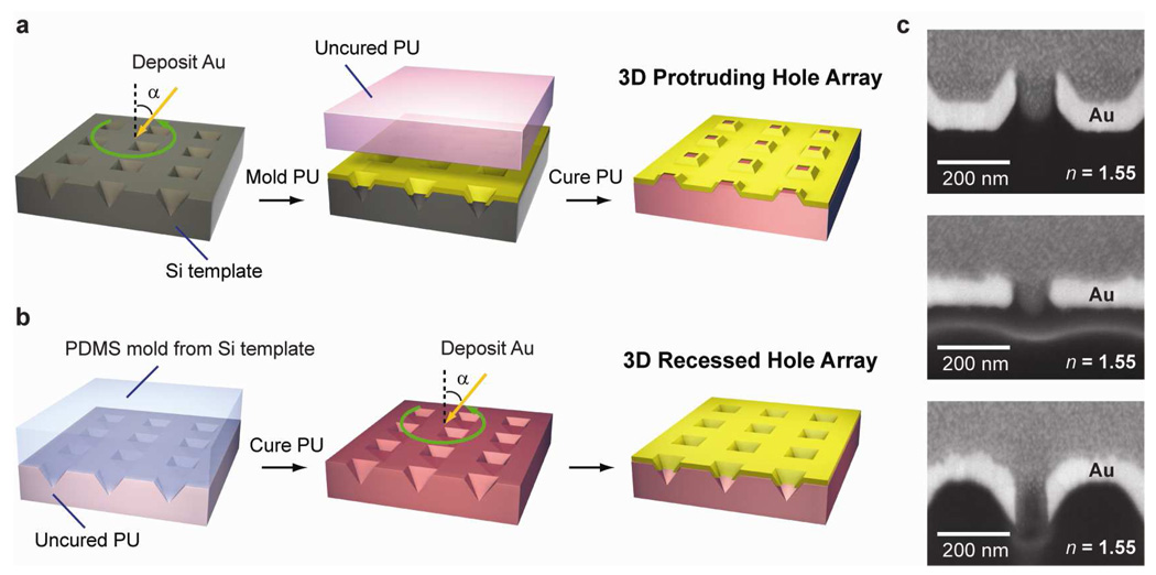
Figure 1 summarizes how metal films perforated with 3D nanoholes were fabricated from templates of nanopyramidal pits followed by metal deposition at oblique angles. Protruding 3D nanohole arrays (tapered ends pointing away from the substrate) were fabricated by deposition of gold (Au) at specific angles (α) on a silicon (Si) template followed by template-stripping14 using UV-curable polyurethane (PU) as the transfer material (Fig. 1a). PU replicas of the Si template were formed by first molding poly(dimethylsiloxane) (PDMS) against the Si nanopatterns and then molding the patterned PDMS against PU (Fig. 1b). Recessed 3D hole arrays (tapered ends pointing toward the substrate) were generated by the angled deposition of Au directly on the PU template (Fig. 1b). For both 3D nanohole arrays, the array spacing was 400 nm (Fig. S1), and the substrate was optically transparent PU (n = 1.55). Figure 1c highlights how geometric features of the 3D hole shapes are different from 2D circular ones for identical film thicknesses (Methods). Focused ion beam (FIB) cross-sections revealed that the tapered ends were extremely sharp because of shadowing by the edges of the nanopyramidal pits during metal deposition. Similar to the 2D holes, the tapered ends of the 3D holes had openings of 100 nm; the other ends, however, were 220 nm and corresponded to the nanopyramid template edge length. Tapered openings with different sizes were achieved by increasing α > 35° (the complementary angle between Si (100) and Si (111) surfaces) (Fig. S2).
Figure 1. Fabrication of 3D nanohole arrays.
(a) 3D protruding hole arrays fabricated by metal deposition at α = 60° on a nanopyramidal Si template followed by template stripping. (b) 3D recessed hole arrays produced by metal deposition on a PU (polyurethane) substrate replicated from the Si template in (a). (c) (top to bottom) FIB cross-sections of 3D protruding, 2D planar, and 3D recessed hole arrays. The granular layer above the Au film was Pt/carbon, which was deposited to protect the surface before ion beam milling. The images have been corrected a tilt angle of 52°.
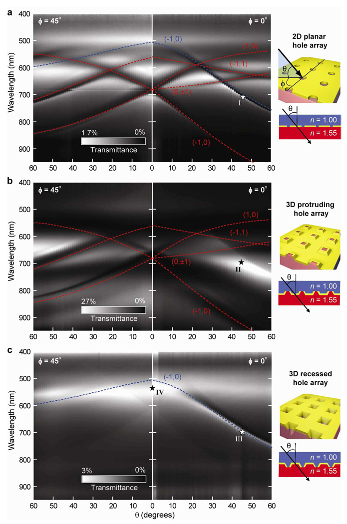
Because fabrication techniques based on molding can create 3D nanohole arrays over cm2-areas with high uniformity (Fig. S3), optical transmission spectra can be acquired over a wide range of excitation angles (θ = 0° to 60°). Figure 2 depicts the differences among angle-resolved transmission spectra for 2D and 3D nanohole arrays at two different azimuthal angles (ϕ). As expected, independent of illumination direction (light incident from either the substrate or the superstrate side of the metal film), identical zero-order transmission spectra for all nanohole arrays were observed (not shown). This reciprocity has also been reported for 2D planar nanohole arrays made by FIB.12, 13 Similar to other measurements,12, 13, 15 transmission through 2D hole arrays supports SPPs from the Au-substrate interface (red curves) and the Au-superstrate interface (blue curves) (Fig. 2a). We identified five SPP bands based on the Bragg coupling relation:13 (−1, 0) modes from Au-substrate and Au-superstrate interfaces that shifted to longer wavelengths as θ increased; (−1, 1) and (0, ±1) modes from the Au-substrate interface that started to emerge at θ = 20°; and a (1, 0) mode from the Au-substrate interface that shifted to shorter wavelengths as θ increased. No SPP modes were observed at wavelengths shorter than the interband transition of Au (~500 nm).
Figure 2. 3D nanohole arrays show strong LSP-mediated transmission and suppress SPP modes.
Angle-resolved optical transmission maps of (a) planar, (b) protruding and (c) recessed hole arrays measured in air under p-polarized white light. Blue dashed curves denote SPP modes from the superstrate (air). Red dashed curves show SPP modes from the substrate (PU). θ is the incident angle of light, and ϕ is the azimuthal angle. I–IV are locations of specific interest. Strong LSP-medicated transmission occurs at II and IV, while SPP modes associated with the tapered end of the 3D holes are absent.
The transmission from the anisotropic 3D hole arrays was different compared to the 2D hole arrays. Strikingly, SPPs were absent at the Au-superstrate interface of the 3D protruding hole arrays (Fig. 2b) as well as at the Au-substrate interface of the 3D recessed hole arrays (Fig. 2c). Thus, SPP modes at the interface between the dielectric materials and the tapered ends of holes were suppressed for all excitation angles. Although the ratio of indented to raised areas on one-dimensional gratings has resulted in changes in SPP coupling efficiency,16, 17 the elimination of SPP modes at a single metal-dielectric interface has not been reported. We calculated optical transmission spectra using the finite-difference time-domain (FDTD) method to verify the suppression of SPPs at the tapered nanohole openings (Methods). Excellent agreement with experiment was observed (Fig. S4).
The intensity maps of the angle-resolved transmission spectra also showed regions with high optical transmission for 3D hole arrays. For protruding hole arrays, regions of high transmission emerged at high excitation angles (θ > 30°) between 600 and 800 nm (Fig. 2b). For recessed 3D hole arrays, the broad transmission region was centered around 530 nm (Fig. 2c). Other key characteristics included (1) the area was spectrally non-dispersive (the wavelength did not shift with θ and ϕ); and (2) the intensity was higher than that of the SPP (−1, 0) mode at all angles (Fig. 2c). The broadband features were also reproduced by FDTD calculations (Figs. S4a–b) and characteristic of LSPs.18
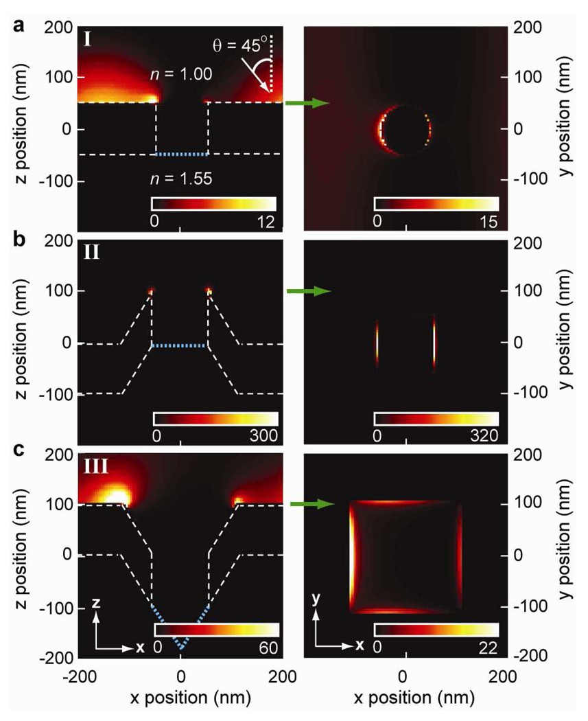
Figure 3 depicts the calculated electric field intensities (|Ez|2) of the three hole arrays under similar excitation angles and wavelengths (I, II, and III in Fig. 2). |Ez|2 of the 2D planar and 3D recessed hole arrays near λ = 695 nm showed characteristic evanescent fields from SPPs with a decay length exceeding 100 nm (Figs. 3a and 3c). In contrast, a LSP was identified at the sharp, tapered edges of the 3D protruding hole with the field intensity orders of magnitude higher (Fig. 3b). Figure S5 indicates that LSPs are also present on the recessed hole arrays (λ = 530 nm, IV in Fig. 2), although the behavior of the LSPs on the protruding and recessed 3D nanohole arrays is very different. LSPs supported by the protruding hole arrays were dispersive.
Figure 3. Strong LSPs are generated on protruding hole arrays under oblique excitation.
Electric field intensities (|Ez|2) calculated by FDTD on (a) planar hole arrays at λ (I) = 705 nm, (b) protruding hole arrays at λ (II) = 695 nm, and (c) recessed hole arrays at λ (III) = 700 nm from Fig. 2. The white dashed lines outline the metal-dielectric interface. The blue dotted lines depict the air-PU interface. The green arrows show the z position of the x-y plane images.
We measured angle-resolved spectra under s-polarized light to discriminate between the two LSP trends (Fig. S6). Under s-polarization, SPP modes should not be generated efficiently13, 19 (Methods). In the recessed hole arrays, the SPP (−1, 0) band was absent, and the transmission region associated with the LSPs had an intensity similar to that under p-polarized excitation (Fig. S6b). In the protruding hole arrays, the SPP bands as well as the dispersive LSP region were absent (Fig. S6a). Therefore, the excitation of LSPs in 3D unit cells depends on both the surface geometry and the direction of the electric field.
Enhanced optical transmission (EOT) through subwavelength 2D hole arrays is usually measured under normal incidence (θ = 0°) by either normalizing the measured transmittance to the geometric open area of the hole array12 or to the transmission through randomly spaced holes.20 The 3D nanohole arrays, however, show increased transmission at high excitation angles, where the “line-of-sight” open area is reduced to zero when θ > 40°. Hence, we report not the absolute EOT but (1) the relative enhancement of 3D hole arrays over 2D hole arrays with the same hole size and film thickness; and (2) the enhancement of LSPs over SPPs on the same hole array. For the protruding hole arrays, the transmittance at θ = 45° and λ = 695 nm (II in Fig. 2b) was 24%, which is 14 times higher than that of the 2D planar hole arrays at the same θ and similar λ (the location near the SPP (−1, 0) resonance). Calculated Poynting vector maps showed that fields localized on the tapered end of the 3D holes facilitate energy flow through the holes (Fig. S7). For the recessed hole arrays, the LSP peak was of higher intensity than the SPP (−1, 0) mode at all angles (Fig. 2c), and with an amplitude up to 58% higher at θ = 60° (Fig. S8). LSP-enhanced energy flow inside the holes was also observed in calculations (Fig. S5c). Thus, LSP excitations in 3D hole arrays contribute more to transmission at oblique excitation angles than SPPs.
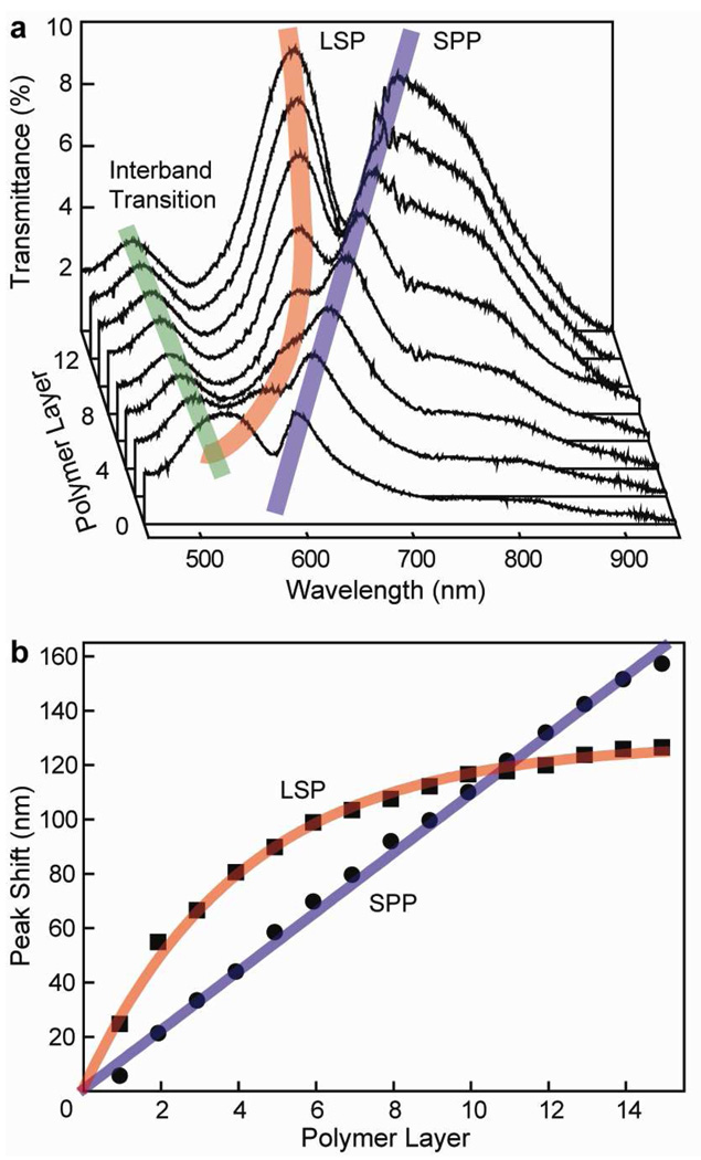
FDTD calculations and angle-resolved spectra indicate that 3D hole arrays can support both LSPs and SPPs on the same substrate; this tunability is not possible by tailoring only the in-plane structure of the hole arrays. As additional confirmation, we characterized the response of the two types of plasmons to changes in the local environment. By depositing polymers with controlled thicknesses on 3D recessed hole arrays (Methods), we verified the differences in the characteristic decay lengths of SPPs and LSPs because of the difference in surface sensitivities.21 Figure 4a shows how the LSP peak and the SPP (−1, 0) resonance respond differently as the surface refractive index is increased. As expected, the SPP response as a function of increased polymer film thickness was linear. This decay length (> 300 nm) was much longer than that of the LSP, whose wavelength shift saturated at about 11 layers (ca. 60 nm) (Fig. 4b). Interestingly, this LSP decay length is longer than that observed from single nanoparticles or nanoparticles in an array (< 30 nm).22, 23
Figure 4. Different plasmon resonances on the same 3D hole array show different spectral shifts.
(a) Transmission spectra from recessed hole arrays as a function of number of polymer layers (θ = 20°, ϕ = 0°). (b) Peak shifts of the LSP peak and SPP (−1,0) resonance. The SPP resonance showed a linear response with respect to the number of polymer layers while the LSP response saturated after 11 layers. The thickness of each layer is about 6 nm.
In summary, we have constructed 3D nanohole arrays whose high optical transmission is mediated more by LSP excitations than by SPPs. This new plasmonic substrate can generate and control independently both strong LSPs and expected SPPs. We anticipate that 3D, anisotropic nanohole arrays will find use in a range of optical devices, from plasmon-enhanced, broadband photovoltaics to label-free biosensors with multiple sensing channels displaying different surface sensitivities.
Methods
Fabrication
The planar 2D nanohole arrays and Si templates with etched pyramidal pits were prepared using SIL followed by PEEL.10, 24 In brief, 100-nm diameter photoresist posts (Shipley 1805) were patterned on a 400-nm pitch on a Si (100) wafer. A 20-nm thick layer of Cr was deposited by e-beam on the pattern, and then the photoresist was lifted off to reveal 100-nm holes on Cr. These holes were used as masks for an anisotropic KOH etch on the underlying Si (100). Pyramidal pits were formed beneath the Cr holes with four intersecting Si (111) faces. After the Cr layer was dissolved, free-standing Au films with 2D nanoholes arrays as well as Si templates with etched pyramidal pits were formed. 5 µL of UV-curable polyurethane (NOA61, Norland Product Inc., NJ) was placed on the nanohole film and then covered by a glass slide. The nanohole film was secured on the glass substrate with cured polyurethane after exposed under 100-W UV lamp for 15 min.
After cleaning by acetone, piranha solution (3:1 H2SO4: 30% H2O2), and DI water, the Si template was mounted on a stage that can tilt between 0° and 90°. Au was deposited by e-beam on the template with an angle (α) ranging from 40° to 60°. The Au vapor could not reach the apex of the pyramidal pits if α > 35.26° – the complementary angle between Si (100) and Si (111). The stage was rotated at 300 rpm. 5 µL of PU was placed on the as-deposited metal films, covered by a glass slide, placed in vacuum (300 mtorr) for 5 min, and then cured by UV light for 15 min. The Au film could be stripped off easily by separating the Si template and glass slides to create protruding 3D hole arrays.
For the recessed hole arrays, h-PDMS molds of the Si templates were first generated.10, 25 PU replicas were prepared by placing 5 µL of PU on the h-PDMS mold and curing by UV irradiation for 15 min. Multiple PU replicas could be created from a single mold. Au was then deposited on the substrate at an oblique angle to create recessed 3D hole arrays.
Optical measurements
The hole array film was mounted on a computer-controlled stage that can rotate from 0°-360° with 0.02° accuracy. Collimated p-polarized or s-polarized white light from a 100-W halogen source was incident on the nanohole array and the transmitted light was directed to a spectrometer (Triax 522/LN2-cooled CCD, Horiba Jobin Yvon).
SPP calculation
The calculation was performed using the surface plasmon polariton-Bloch wave (SPP-BW) model:13, 24
where ω, c, and k0 are the angular frequency, speed, and momentum of light in free-space. εd and εm are frequency-dependent relative permittivity of the adjacent dielectric material and metal (gold), which was taken from Johnson and Christy.26 θ is the incident angle, and ϕ is the azimuthal angle. Gx and Gy are Bragg vectors associated with two periodicity of the array, and Bragg index (i, j) denote specific SPP modes. Here Gx = Gy = 2π/a0, where a0 is the periodicity of arrays.
FDTD simulations
We performed 3D finite difference time domain (FDTD) simulations using commercial software (FDTD solution, Lumerical Inc. Vancouver, Canada). A uniform mesh size of 4 nm (x, y, and z directions) was chosen. The optical constants of materials were taken from Johnson and Christy26 in the spectrum range from 400 nm to 1000 nm. The dielectric dispersion profiles of the materials were fitted by the multi-coefficient model that relies on an extensive set of basis functions. To calculate angle and frequency dependent transmittance, PML (perfectly matched layer) boundary conditions were set for the z direction, and Bloch boundary conditions were applied to x and y directions of the simulation region.
Multilayer polymer adsorption.25, 27, 28
The gold sensing surface was first incubated in 2-mM ethanolic solution of carboxyl-terminated thiol (HS-(CH2)11-COOH, Sigma-Aldrich) for 16 h to form an ordered monolayer. DNA (0.2 mg/mL sodium salt from calf thymus, Sigma-Aldrich) and poly(dimethyldiallylammonium chloride) (0.5 mg/mL, MW = 4–5 × 10⁵ Da, Sigma-Aldrich) in PBS buffer (pH = 7.0) were subsequently dropped on the substrate alternatively to form stable polymer layers. Spectra were taken after adsorbing the DNA layers. The thickness of the polymer layer was determined by profilometry and ellipsometry.
Supplementary Material
Acknowledgments
This work was supported by the National Science Foundation (NSF) under NSF Award Number CMMI-0826219, NSF DMR-0705741, Northwestern University’s Cancer Center for Nanotechnology Excellence (NCI U54CA119341), and the NIH Director’s Pioneer Award (DP1OD003899). This work made use of the NUANCE Center facilities, which are supported by NSF-MRSEC, NSF-NSEC and the Keck Foundation.
Footnotes
Supporting Information Available: SEM images of hole arrays; FDTD calculated angle-resolved optical transmission, electric field distribution, and Poynting vector maps; optical transmission under s-polarized light. This material is available free of charge via the Internet at http://pubs.acs.org.
References
- 1.Ebbesen TW, Lezec HJ, Ghaemi HF, Thio T, Wolff PA. Nature. 1998;391:667–669. [Google Scholar]
- 2.Genet C, Ebbesen TW. Nature. 2007;445:39–46. doi: 10.1038/nature05350. [DOI] [PubMed] [Google Scholar]
- 3.Huang FM, Kao TS, Fedotov VA, Chen YF, Zheludev NI. Nano Lett. 2008;8:2469–2472. doi: 10.1021/nl801476v. [DOI] [PubMed] [Google Scholar]
- 4.Dennis MR, Zheludev NI, de Abajo FJ. Opt. Express. 2007;15:9692–9700. doi: 10.1364/oe.15.009692. [DOI] [PubMed] [Google Scholar]
- 5.Chowdhury MH, Catchmark JM, Lakowicza JR. Appl. Phys. Lett. 2007;91:3. doi: 10.1063/1.2783177. [DOI] [PMC free article] [PubMed] [Google Scholar]
- 6.Koerkamp KJK, Enoch S, Segerink FB, van Hulst NF, Kuipers L. Phys. Rev. Lett. 2004;92 doi: 10.1103/PhysRevLett.92.183901. [DOI] [PubMed] [Google Scholar]
- 7.van der Molen KL, Klein Koerkamp KJ, Enoch S, Segerink FB, van Hulst NF, Kuipers L. Phys. Rev. B. 2005;72 [Google Scholar]
- 8.Matsui T, Agrawal A, Nahata A, Vardeny ZV. Nature. 2007;446:517–521. doi: 10.1038/nature05620. [DOI] [PubMed] [Google Scholar]
- 9.Billaudeau C, Collin S, Sauvan C, Bardou N, Pardo F, Pelouard JL. Opt. Lett. 2008;33:165–167. doi: 10.1364/ol.33.000165. [DOI] [PubMed] [Google Scholar]
- 10.Henzie J, Lee MH, Odom TW. Nature Nanotech. 2007;2:549–554. doi: 10.1038/nnano.2007.252. [DOI] [PubMed] [Google Scholar]
- 11.Odom TW, Gao HW, McMahon JM, Henzie J, Schatz GC. Chem. Phys. Lett. 2009;483:187–192. [Google Scholar]
- 12.Ghaemi HF, Thio T, Grupp DE, Ebbesen TW, Lezec HJ. Phys. Rev. B. 1998;58:6779–6782. [Google Scholar]
- 13.Barnes WL, Murray WA, Dintinger J, Devaux E, Ebbesen TW. Phys. Rev. Lett. 2004;92 doi: 10.1103/PhysRevLett.92.107401. [DOI] [PubMed] [Google Scholar]
- 14.Nagpal P, Lindquist NC, Oh SH, Norris DJ. Science. 2009;325:594–597. doi: 10.1126/science.1174655. [DOI] [PubMed] [Google Scholar]
- 15.Gao H, McMahon JM, Lee MH, Henzie J, Gray SK, Schatz GC, Odom TW. Opt. Express. 2009;17:2334–2340. doi: 10.1364/oe.17.002334. [DOI] [PubMed] [Google Scholar]
- 16.Leveque G, Martin OJF. J. Appl. Phys. 2006;100 [Google Scholar]
- 17.Giannattasio A, Hooper IR, Barnes WL. Opt. Commun. 2006;261:291–295. [Google Scholar]
- 18.Kelf TA, Sugawara Y, Baumberg JJ, Abdelsalam M, Bartlett PN. Phys. Rev. Lett. 2005;95:4. doi: 10.1103/PhysRevLett.95.116802. [DOI] [PubMed] [Google Scholar]
- 19.Zayats AV, Smolyaninov II, Maradudin AA. Phys. Rep. 2005;408:131–314. [Google Scholar]
- 20.Pacifici D, Lezec HJ, Sweatlock LA, Walters RJ, Atwater HA. Opt. Express. 2008;16:9222–9238. doi: 10.1364/oe.16.009222. [DOI] [PubMed] [Google Scholar]
- 21.Willets KA, Van Duyne RP. Annu. Rev. Phys. Chem. 2007;58:267–297. doi: 10.1146/annurev.physchem.58.032806.104607. [DOI] [PubMed] [Google Scholar]
- 22.Sannomiya T, Sahoo PK, Mahcicek DI, Solak HH, Hafner C, Grieshaber D, Voros J. Small. 2009;5:1889–1896. doi: 10.1002/smll.200900284. [DOI] [PubMed] [Google Scholar]
- 23.Murphy CJ, Gole AM, Hunyadi SE, Stone JW, Sisco PN, Alkilany A, Kinard BE, Hankins P. Chem. Commun. 2008:544–557. doi: 10.1039/b711069c. [DOI] [PubMed] [Google Scholar]
- 24.Gao HW, Zhou W, Odom TW. Adv. Funct. Mater. 2010;20:529–539. [Google Scholar]
- 25.Gao HW, Yang J-C, Lin JY, Stuparu AD, Lee MH, Mrksich M, Odom TW. Nano Lett. 2010 doi: 10.1021/nl101165r. ASAP. [DOI] [PubMed] [Google Scholar]
- 26.Johnson PB, Christy RW. Phys. Rev. B. 1972;6:4370–4379. [Google Scholar]
- 27.Otte MA, Sepulveda B, Ni WH, Juste JP, Liz-Marzan LM, Lechuga LM. ACS Nano. 2010;4:349–357. doi: 10.1021/nn901024e. [DOI] [PubMed] [Google Scholar]
- 28.Pei RJ, Cui XQ, Yang XR, Wang EK. Biomacromolecules. 2001;2:463–468. doi: 10.1021/bm0001289. [DOI] [PubMed] [Google Scholar]
Associated Data
This section collects any data citations, data availability statements, or supplementary materials included in this article.


