Abstract
We report a new method for fabricating an optofluidic waveguide that is compatible with polydimethylsiloxane (PDMS). The light path follows the microfluidic channels, an architecture that can maximize detection efficiency and make the most economic use of chip area in many lab-on-chip applications. The PDMS-based microfluidic channels are coated with Teflon amorphous fluoropolymers (Teflon AF) which has a lower refractive index (n = 1.31) than water (n = 1.33) to form a water/Teflon AF optical waveguide. Driven by a vacuum pump, the Teflon AF solution was flowed through the channels, leaving a thin (5–15 µm) layer of coating on the channel wall as the cladding layer of optical waveguides. This coating process resolves the limitations of spin-coating processes by reducing the elasticity mismatch between the Teflon AF cladding layer and the PDMS device body. We demonstrate that the resulting optofluidic waveguide confines and guides the laser light through the liquid core channel. Furthermore, the light in such a waveguide can be split when the fluid flow is split. This new method enables highly integrated biosensors such as lab-on-chip flow cytometers and micro-fabricated fluorescence-activated cell sorter with on-chip excitation.
Index Terms: Polymer waveguides, sensors, Teflon amorphous fluoropolymers (Teflon AF)
Optofluidics is an emerging field that integrates microfluidics and optics on the same device to work synergistically [1]. Devices that contain both microfluidic channels and on-chip photonic circuits, such as integrated biochemical sensors, show enhanced functionality and sensitivity and enable significant cost and size reduction. Many research groups have demonstrated that fluidic channels and optical waveguides can be fabricated on the same substrate [2], [3]. In order to assure that photons and biological samples in the fluid interact most effectively for the highest sensitivity, however, we desire the flexibility to direct and align the paths of light and fluid. In some cases, we need light beams to intersect the fluidic channels to localize the interrogation area [4]. In other cases, we want the light wave and the fluid to share the same path to maximize their interaction. For the latter case, we still lack an effective fabrication method. Due to the fact that most polymers used in lab-on-a-chip devices have a higher index of refraction than water, light traveling in the fluidic channel will not be confined, suffering from high radiation loss. In this work, we report a polydimethylsiloxane (PDMS)-compatible process of coating microfluidic channels with a layer of low refractive index Teflon amorphous fluoropolymers (Teflon AF) solution, enabling the water in the fluidic channel to be used as the waveguide’s high index core. We further show that the Teflon AF-coated waveguide works not only for straight fluidic channels but also for split channels. In addition to delivering the light, by Teflon coating the microfluidic channel, we also create a channel with low sample adsorption, avoiding a troublesome problem found in many polymer-based microfluidic devices.
Teflon AF is an amorphous fluoropolymer that is chemically stable and optically transparent from ultraviolet (UV) to infrared wavelengths. Unlike other fluoropolymers, Teflon AF has a refractive index (n = 1.31) that is lower than the index of water (n = 1.33) therefore, a Teflon AF coating layer can be used to clad a liquid-core optical waveguide. Light will then be delivered through the same physical path as the fluid flows by total internal reflection when the coated channels are filled with water or aqueous solutions. Datta et al. reported the fabrication of Teflon-coated liquid core waveguides by spin-coating a Teflon AF solution onto silicon or glass substrates in 2003 [5]. The fabrication process for these glass substrates, however, is relatively expensive and time consuming. If the Teflon AF coating process can be applied to polymers such as PDMS, a favored material for developing many of today’s microfluidic devices, it can be an attractive process for use in lab-on-chip devices. Guo et al. fabricated a Teflon AF-coated liquid core waveguide by spin-coating Teflon AF on PDMS substrates [6]. However, the spin-coating of Teflon AF onto a PDMS substrate has its limitations. One challenge of the spin-coating process is that once the Teflon AF coating is formed on PDMS substrates, bonding between Teflon AF layers becomes very difficult, as Teflon AF (like any Teflon material) is chemically stable. Bonding between Teflon AF coating layers was reported by using physical clamping at temperatures above 330 °C [6]. At this temperature, PDMS (e.g., Sylgard 184) turns brown and loses its optical transparency. In addition, surface cracking often results during device process and handling, as the elastic modulus of Teflon AF is about 1000 times that of PDMS [7]. In order to resolve aforementioned limitations, we demonstrate a new procedure for coating Teflon AF onto the PDMS channel walls by flowing Teflon AF solution through the microchannel, thereby creating the cladding layer for an optical waveguide along the path of fluid flow. The light introduced to microchannels is confined inside the core of the waveguide (i.e., microfluidic channel) and guided by fluid flowing through the channel.
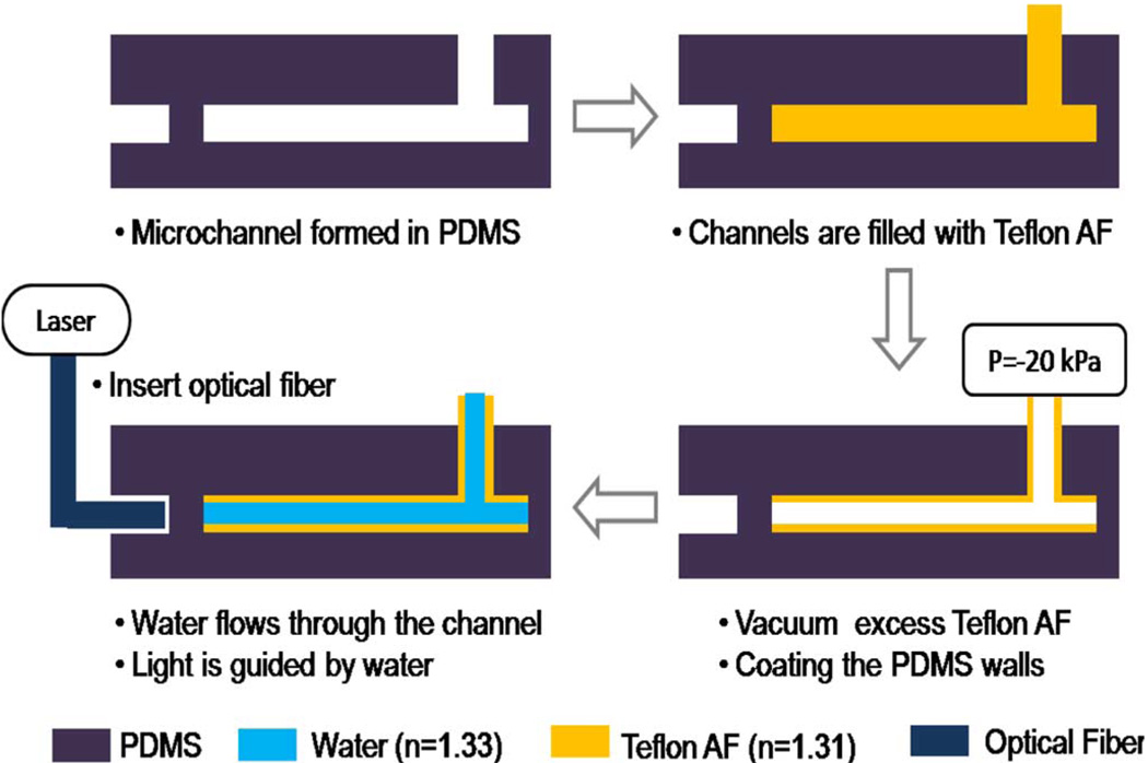
Microfluidic channels that are 200 µm by 70 µm are fabricated in PDMS. A master mold is lithographically defined on an optically smooth Si wafer using SU-8 50 (MicroChem). Two replicas are created: one replica with microfluidic channels and one replica of an optically smooth blank Si wafer. A solution of 2% 1H,1H,2H,2H-perfluorodecyltriethoxysilane (Sigma Aldrich Inc.) is spin-coated onto PDMS substrates and heated at 110 °C for 10 min to promote adhesion between PDMS and the Teflon AF solution. Both PDMS surfaces are then activated for permanent bonding by UV/Ozone treatment (UVO-CLEANER 42, Jelight Inc.) for 3 min and bonded together, thus capping the microfluidic channels. A 6% Teflon AF solution (601-S2, DuPont Corp) is flowed into the microfluidic channels. Once they are filled, vacuum (P = −20 kPa) is applied for 20 min to remove excess Teflon AF solution from the channels (see Fig. 1). The balance between the vacuum force and the adhesion to the PDMS channel wall determines the thickness of the cladding layer.
Fig. 1.
Fabrication process for Teflon AF-coated liquid core waveguides. This process reduces the elastic mismatch between PDMS and Teflon AF.
The process results in a smooth channel with a hollow core. The Teflon AF-coated PDMS device is heated to 155 °C for 20 min to evaporate the fluoroinert solvent, and then heated further to 175 °C (15 °C above the its glass transition temperature) for 20 min to form a smooth Teflon AF layer. This relatively low temperature coating is compatible with the PDMS process while significantly reducing the consumption of Teflon solution compared to the spin-coating process. Calculations show that a ~5-µm-thick Teflon AF film is necessary to confine the light to the liquid core [8]. In our work, the cladding thickness is typically 5–15 µm, thick enough to confine and guide light waves. The thickness of the Teflon AF coating layer can be further controlled by adjusting the applied vacuum pressure and concentration of the Teflon AF solution. After slowly cooling the devices to avoid cracking due to thermal mismatch, an optical fiber is inserted into the channel for light coupling. Deionized (DI) water is then introduced into the hollow core to serve as both the sample flow carrier and the core of the optofluidic waveguide.
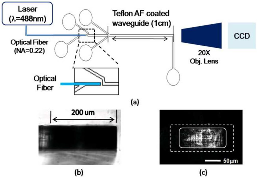
The flowing DI water transports both the suspended samples and the light in the same channel. Fig. 1 illustrates the fabrication process of the Teflon AF-coated optofluidic waveguide. The numerical aperture, of the liquid core waveguide is 0.23, well-matched to the NA of the input multimode fiber (NA = 0.22). The cross section of the liquid core waveguide is imaged by a charged coupled device at the end of the channel, as shown in Fig. 2(a). Fig. 2(b) shows the cross section of the fabricated microfluidic channel that is 200 µm by 70 µm. Fig. 2(c) shows the light output of the optofluidic waveguide when the laser is on. The dotted box shows the wall of the PDMS channel, and the solid line shows the boundary between the Teflon AF cladding layer and the liquid core. It verifies that the light is confined to the liquid core of the optofluidic waveguide by the Teflon AF coating. A waveguide loss of 2.13 dB/cm at 488-nm wavelength is measured. Scattering is the dominant factor compared to light leakage and absorption. With improved smoothness of Teflon AF coating, we believe the waveguide loss can be reduced significantly.
Fig. 2.
(a) Experimental setup for light output measurement. (b) Cross section of the liquid core waveguide. (c) Light output from a liquid core waveguide with Teflon AF coating. The dotted box is the perimeter of the channel, and the solid line is the Teflon AF-coated core layer.
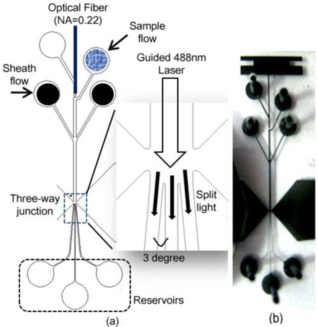
Fig. 3(a) shows the layout of a microfluidic channel which includes a splitting junction, and Fig. 3(b) is a photograph of the device. Laser light (λ = 488 nm) is fiber-coupled into the microfluidic channel, in which water flows. Light is guided by the fluid flow, and at the three-way junction, as shown in the enlarged box in Fig. 3(a), the 488-nm light is divided into three paths following the fluid flow towards the channel outlets. In order to demonstrate that light can be split and guided through three channels, we have filled the device with a diluted Rhodamine 6G solution that emits green fluorescence in all directions after absorption of the guided 488-nm light.
Fig. 3.
(a) Layout of the device. Light can be split and guided at the three-way junction. (b) Photograph of the device fabricated in PDMS.
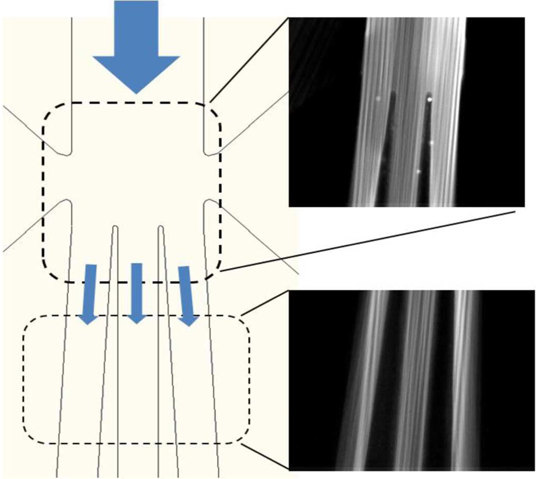
As shown in Fig. 4, the light guided from the upstream channel is divided into three split channels separated by 3°. The result demonstrates that the excitation light is split into three channels and that the split light is still guided through the channels. Since the light always traces the fluid flow in which samples are suspended, excitation is performed at all locations, and thus detection can be performed at any position. This unique property provides a very convenient feature for lab-on-a-chip devices. For example, it becomes possible to perform highly sensitive fluorescence detection at multiple locations using only a single light source, imparting a high degree of design flexibility to miniaturized optofluidic devices, for example, lab-on-chip flow cytometers or micro-fabricated fluorescence-activated cell sorter (µFACS).
Fig. 4.
Light emitted by Rhodamine 6G when the fluorescent dye in the fluid is excited by the 488-nm laser light sharing the same paths as the fluid. We show that the 488-nm input light is guided through the entire paths of fluidic channels, even after the three-way split.
To summarize, we have developed a new fabrication process for shared-path optofluidic waveguides by using Teflon AF to selectively coat the microfluidic channels of our choosing. We choose Teflon AF for its low refractive index relative to water and for its optical transparency. Our new Teflon AF coating process is compatible with PDMS (one of the most popular polymers in microfluidics) in that the process removes the elasticity mismatch between Teflon AF and PDMS and preserves both the optical and physical properties of PDMS that make it desirable for many microfluidic applications. In addition, the process requires only a small amount of Teflon AF solution (less than 20 µl). This enables optofluidic waveguides to be fabricated in PDMS in a cost-effective, less time-consuming manner. The coating created by our process is tunable via adjustment of the dilution (viscosity) of the Teflon AF solution and also by force applied by the vacuum. In addition, since Teflon AF is chemically stable, our process further circumvents common issues with sample absorption at the wall of the microfluidic channel. Furthermore, we demonstrate that as the fluid path is split, so is the light path, creating a fluidically controlled optical circuit. This technology offers design flexibility and efficient interactions between light and samples for lab-on-a-chip devices.
ACKNOWLEDGMENT
The authors acknowledge the technical support of the staff of the UCSD Nano3 (nanoscience, nanoengineering, and nanomedicine) Facility in CALIT2.
The work was supported by the NIH under Grant 1R01HG004876 and Grant 1R21RR024453.
Contributor Information
Sung Hwan Cho, Materials Science and Engineering Program, University of California at San Diego, La Jolla, CA 92093-0418 USA (scho@logroup.ucsd.edu)..
Jessica Godin, Electrical and Computer Engineering Department, University of California at San Diego, La Jolla, CA 92093-0407 USA..
Yu-Hwa Lo, Electrical and Computer Engineering Department, University of California at San Diego, La Jolla, CA 92093-0407 USA..
REFERENCES
- 1.Psaltis D, Quake SR, Yang C. Developing optofluidic technology through the fusion of microfluidics and optics. Nature-London. 2006;vol. 442:381–381. doi: 10.1038/nature05060. [DOI] [PubMed] [Google Scholar]
- 2.Chang-Yen DA, Eich RK, Gale BK. A monolithic PDMS waveguide system fabricated using soft-lithography techniques. J. Lightw. Technol. 2005 Jun;vol. 23(no. 6):2088–2093. [Google Scholar]
- 3.Lien VB, Lo YYH. A prealigned process of integrating optical waveguides with microfluidic devices. IEEE Photon. Technol. Lett. 2004 Jun;vol. 16(no. 6):1525–1527. [Google Scholar]
- 4.Godin J, Lien V, Lo YH. Demonstration of two-dimensional fluidic lens for integration into microfluidic flow cytometers. Appl. Phys. Lett. 2006;vol. 89:061106. [Google Scholar]
- 5.Datta A, Eom IY, Dhar A, Kuban P, Manor R, Ahmad I, Gangopadhyay S, Dallas T, Holtz M, Temkin H. Microfabrication and characterization of Teflon AF-coated liquid core waveguide channels in silicon. IEEE Sensors J. 2003 Dec;vol. 3(no. 6):788–795. [Google Scholar]
- 6.Wu CW, Gong GC. Fabrication of PDMS-based nitrite sensors using Teflon AF coating microchannels. IEEE Sensors J. 2008 May;vol. 8(no. 5):465–469. [Google Scholar]
- 7.Loetters JC, Olthuis W, Veltink PH, Bergveld P. The mechanical properties of the rubber elastic polymer polydimethylsiloxane for sensor applications. J. Micromech. Microeng. 1997;vol. 7:145–147. [Google Scholar]
- 8.Dress P, Belz M, Klein KF, Grattan KTV, Franke H. Physical analysis of Teflon coated capillary waveguides. Sens. Actuators B, Chem. 1998;vol. 51:278–284. [Google Scholar]


