Abstract
A modified Cartesian feedback method called “frequency-offset Cartesian feedback” and based on polyphase difference amplifiers is described that significantly reduces the problems associated with quadrature errors and DC-offsets in classic Cartesian feedback power amplifier control systems.
In this method, the reference input and feedback signals are down-converted and compared at a low intermediate frequency (IF) instead of at DC. The polyphase difference amplifiers create a complex control bandwidth centered at this low IF, which is typically offset from DC by 200–1500 kHz. Consequently, the loop gain peak does not overlap DC where voltage offsets, drift, and local oscillator leakage create errors. Moreover, quadrature mismatch errors are significantly attenuated in the control bandwidth. Since the polyphase amplifiers selectively amplify the complex signals characterized by a +90° phase relationship representing positive frequency signals, the control system operates somewhat like single sideband (SSB) modulation. However, the approach still allows the same modulation bandwidth control as classic Cartesian feedback.
In this paper, the behavior of the polyphase difference amplifier is described through both the results of simulations, based on a theoretical analysis of their architecture, and experiments. We then describe our first printed circuit board prototype of a frequency-offset Cartesian feedback transmitter and its performance in open and closed loop configuration. This approach should be especially useful in magnetic resonance imaging transmit array systems.
Index Terms: Cartesian feedback, control systems, mixers, polyphase amplifiers, RF power amplifiers
I. INTRODUCTION
Radiofrequency power amplifiers are used in a wide variety of applications including but not limited to wireless communications and magnetic resonance imaging (MRI).
The specifications for such diverse applications are indeed different, but they have one common denominator: the need to maximize both the efficiency and linearity of increasingly powerful amplifiers. In the field of communications, linearity is demanded by the desire for high spectral efficiency, that is, the ability to transmit data at the highest possible rate for a given channel bandwidth [1], [2]. In the field of MRI, it is the increasingly popular use of arrays of coils that challenges the linearity of the power amplifiers driving these coils, because of coil coupling that changes the amplifier load conditions (and induced output currents) significantly and unpredictably [3], [4]. Many different linearization techniques have been proposed to deal with these challenges. Among them, Cartesian feedback has been proposed in both fields and has received a great deal of attention thanks to the advantage that it does not require a detailed knowledge of the power amplifier behavior and is immune to changes such as those due to temperature and aging [5]–[10]. While there is a strong theoretical motivation to pursue Cartesian feedback, its penetration into both fields has been held back by the complexities associated with the actual implementation of the system. Issues such as the impact of phase misalignment on stability, phase and amplitude quadrature errors (particularly in the down-converter of the feedback path), and DC-offsets (particularly at the output of the multipliers and at the input of the error amplifiers, also called loop difference amplifiers) have been and still are the subject of many studies [11]–[17]. The limit imposed by the accuracy of the down-conversion is fundamental to linearization strategies, as errors in the feedback path cannot be compensated by the loop operation and further complicate the analysis of the phase alignment control problem [18]. DC-offsets also impact the quality of the output baseband spectrum.
We have developed a modified Cartesian feedback architecture that we call frequency-offset Cartesian feedback (FOCF) that significantly reduces or eliminates the problems associated with quadrature errors and DC-offsets. In the FOCF system, the reference input and the feedback signal are both down-converted and subtracted at a low intermediate frequency (IF) band instead of at DC. From a circuit standpoint, the modification affects only the loop difference amplifier. While the classic Cartesian feedback (CCF) architecture employs matched baseband low-pass difference amplifiers, we propose the use of a complex-bandpass (polyphase) difference amplifier as a way to shift the control bandwidth to this low IF. This enables a significant relaxation of the specifications of the circuit blocks, and can decrease the complexity of the system implementation, without impairing the linearization performance of the feedback loop. Since the polyphase amplifiers selectively amplify the complex signals characterized by a +90° phase relationship representing positive frequency signals, the control system operates somewhat like single sideband (SSB) modulation. However, the approach still allows the same modulation bandwidth control as classic Cartesian feedback. In this paper, we discuss the frequency offset Cartesian feedback (FOCF) architecture: its behavior, modeling, and experimental results to assess their performance for use in Cartesian feedback systems. We also present our first prototype FOCF system and preliminary results of open and closed loop testing.
II. CLASSIC CARTESIAN FEEDBACK
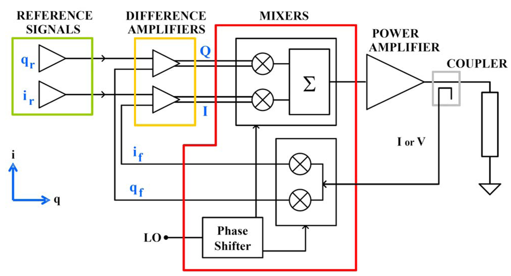
Cartesian feedback is a method of linearising radio-frequency (RF) power amplifiers. The basic architecture of a Cartesian Feedback system is shown in Fig. 1.
Fig. 1.
Basic architecture of the classic Cartesian feedback method.
The quadrature baseband inputs, usually termed the i and q components, form the reference signals for the loop. The forward path consists of the difference amplifiers, the synchronous up-mixer, the non-linear power amplifier, and the output load (usually an antenna). The difference amplifiers are characterized, to first order approximation, by the transfer function HC(ω) that describes the relationship between the complex output I+jQ and the complex input i+jq. Dawson and Lee [18] emphasize the importance of choosing HC(ω) = k/sx where 0 < x < 1, as a compensation strategy for robustness to phase misalignments that impact stability, however these “slow-rolloff" functions are not truly realizable with a lumped-element network and are usually approximated by alternating poles and zeros such that the average slope of HC(s) has the appropriate roll-off. In practice, it is not uncommon to find Cartesian feedback systems in which the difference amplifiers are characterized by as few as one single pole at a frequency ωo other than DC and one single zero at higher frequency, such that the transfer function near DC can be roughly approximated by
| (1) |
where K is the gain of the difference amplifier at DC. The feedback path consists of a coupler that sends a sample of the power amplifier output voltage (or current) to the synchronous down-mixer. The quadrature baseband components that result from this down-conversion are used as feedback signals and compared (subtracted) to the reference signals at the input of the difference amplifiers. The up-converted output of these amplifiers (the loop error signal) is thus the pre-distorted signal necessary to drive and linearise the power amplifier.
The last indispensable component of a Cartesian feedback system is the phase shifter. Synchronism between the up- and down-mixers is obtained by splitting a common RF carrier (the local oscillator, or LO, frequency), however the delays through the feedback and forward paths cause the reference and feedback signals to be phase misaligned, a situation that compromises the stability of the system. The phase shifter is thus necessary to compensate for the delays and maintain the correct relationship that guarantees the loop stability.
One of the major challenges designers of Cartesian feedback systems face is that this method is especially sensitive to phase and amplitude quadrature errors in the mixers and to DC-offsets. The impact that these non-idealities have on the system performance is twofold: 1) they may cause in-band aliasing at the output spectrum of the power amplifier, and 2) they complicate and may even prevent the phase alignment control and, thus, the stability of the system [18].
To understand how undesired frequencies are created in the output spectrum by quadrature errors, an open-loop analysis of the circuit is useful. Consider the case of the loop open at the output of the down-mixer. Let the power amplifier be a perfect, ideal amplification block of gain G. The baseband feedback complex signals, if(t) and qf(t), appear at the down-mixer output as a result of input reference signals ir(t) and qr(t) of time-varying envelope A(t) and modulation frequency ωB. If the up-mixer is error-free and the down-mixer introduces a phase quadrature error φ, then
| (2) |
| (3) |
that is, the overall feedback signal is:
| (4) |
If φ is null, then Sf contains only the desired frequency +ωB; otherwise, a so-called image (or, ghost) frequency −ωB is also produced before the subtraction node.
Since the non-ideality responsible for this unwanted behavior is in the feedback path, it will not be compensated by the loop operation once the loop is closed [2]. For the image rejection ratio (the ratio of the amplitudes of the desired and image frequencies) to be at least 40 dB, it can be shown that the maximum value of the phase error φ is 1.15°. Similarly, the maximum value of amplitude imbalance to obtain the same image rejection ratio is 2%. DC-offsets also result in the appearance of unwanted signals, specifically at the LO frequency, at the input of the power amplifier. The presence of this particular undesired frequency is known as LO-leakage.
III. FREQUENCY-OFFSET CARTESIAN FEEDBACK
As a result of growing interest in transmit array power amplifiers for magnetic resonance imaging (MRI) [19]–[22], we invented a modification to the classic Cartesian feedback architecture to address the amplitude-phase quadrature errors and DC-offsets associated with the imperfections of the mixers and other blocks of the system. Although targeted for MRI, our approach is generally applicable to the problem of Cartesian feedback control of any RF power amplifier.
Our approach uses a complex reference input signal centered at a low positive intermediate frequency (IF) band, and the intended modulation bandwidth also occupies only positive frequencies. The sample of the power amplifier output signal is quadrature down-converted as feedback to this IF band instead of DC. Hence, the loop error amplifier performs the subtraction between the reference input and feedback signals at the IF instead of at DC. The classic (matched-pair) difference amplifiers described by (1) cannot be used in this scenario because their control bandwidth and peak gain are centered at DC. A matched pair of bandpass differential amplifiers centered at the IF are also problematic. The bandpass amplifiers would certainly prevent LO leakage by rejecting DC, but would create two control bands for complex signals centered at the positive and negative IF frequencies. Quadrature image errors would remain. More importantly, because two high gain control bands are generated, the system is potentially unstable as the desired signal and its quadrature mismatches experience different loop phase rotation, thereby demanding different compensation strategies. The optimal solution to the problem of subtracting the reference input and the feedback signal would be a complex bandpass difference amplifier, which would create a single control bandwidth centered at the positive IF only.
In the realm of quadrature signals, a complex passband amplifier does exist and can be synthesized with “active polyphase amplifiers” [23]–[26]. The key modification to the classic Cartesian feedback control loop thus consists in substituting active polyphase difference amplifiers for the classic matched difference amplifiers of the Cartesian feedback system. The net result of this change is to move the loop control bandwidth away from DC (at baseband) and the local oscillator frequency (at RF), so that the undesired frequencies that would be created by both quadrature errors and DC-offsets are outside this bandwidth. By doing so, even if quadrature errors and offsets within the loop are not stringently minimized, they do not impair the performance of the Cartesian feedback system.
IV. POLYPHASE AMPLIFIERS
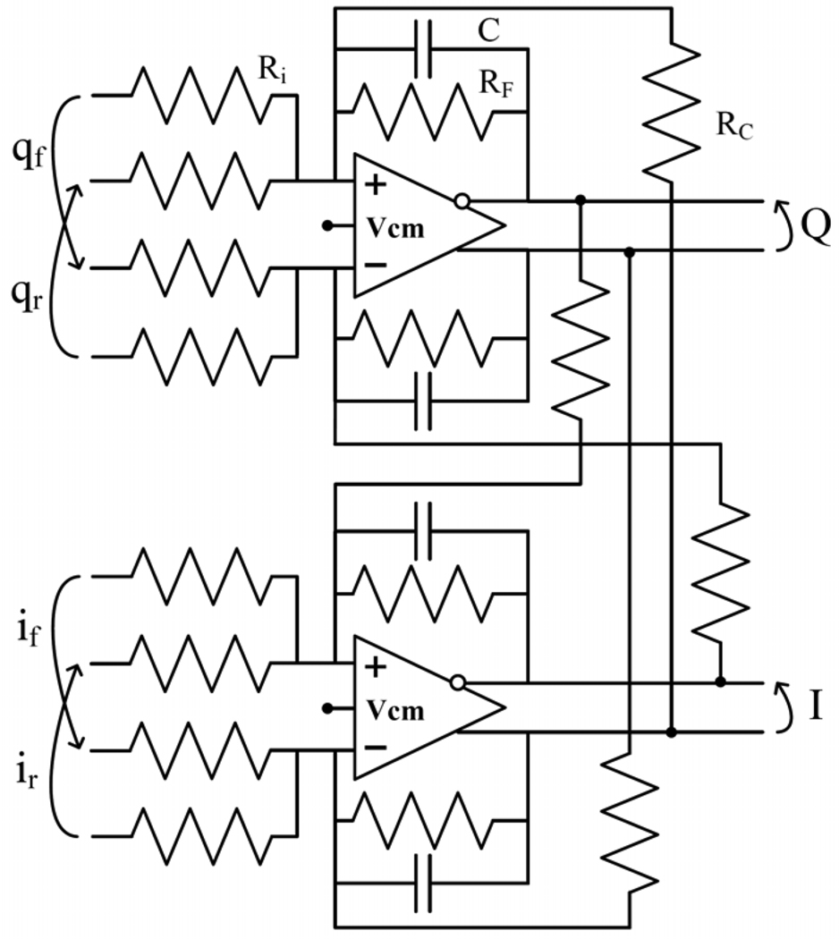
Fig. 2 shows the architecture of the polyphase difference amplifiers, which perform the difference between the pair of quadrature differential reference signals (ir, qr) and quadrature differential feedback signals (if, qf).
Fig. 2.
Simplified schematic of fully differential polyphase difference amplifiers.
As in the classic architecture, the transfer function H(ω) in (5) describes the relationship between the complex output I+jQ and the complex input i+jq of the polyphase architecture, where i = ir − if and q = qr − qf. Here
| (5) |
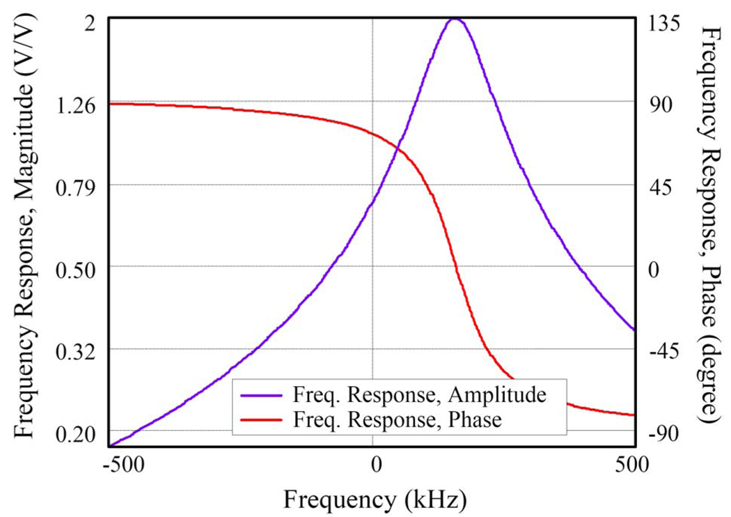
where K = RF·Ri−1, ωc = (RC·C)−1, and ωo = (RF·C)−1 are the peak gain, center frequency, and half width of the baseband signal band, respectively. It is the response of a single pole low pass filter shifted by ωc away from 0 frequency as in Fig. 3. H(ω) is as described by (5) only if its active elements (such as the fully differential operational amplifiers in the discrete implementation) are ideal blocks of infinite gain and bandwidth, its passive components are perfectly matched, and the i and q input signals have the same amplitude and are in perfect quadrature.
Fig. 3.
The frequency response of the ideal polyphase amplifier. (The phase delay at center bandwidth has been set to zero.) Only the desired response is shown; the mirror response is null.
Qualitatively, the polyphase amplifier acts as two asymmetrically cross-coupled amplifiers. The coupling from Q-i is the opposite sign of I-q. A quadrature +/− 90 degree phase relationship representing positive or negative input frequencies leads to constructive or destructive interference in the outputs, and enhanced selectivity of positive frequencies.
An equivalent representation of the operation of polyphase amplifiers can be obtained if one considers the four real input (i, q) to real output (I, Q) transfer functions, and obtains the overall complex response by appropriately combining these functions. Let i2I be the i to I transfer function, q2I the q to I transfer function, q2Q the q to Q transfer function, and i2Q the i to Q transfer function. For a unity-gain polyphase difference amplifier (K is equal to 1), these four equations are
| (6) |
| (7) |
| (8) |
| (9) |
where
| (10) |
This last approach to polyphase amplifier analysis allows us to derive the equations that separate the desired and undesired baseband components of the output response.
Let Up be the positive-frequency response (transfer function) to a positive-frequency input complex signal,
| (11) |
Vp be the negative-frequency response to a positive-frequency input (aka the “mirror” of the desired signal),
| (12) |
Vm be the negative-frequency response to a negative-frequency input,
| (13) |
and Um be the positive-frequency response to a negative-frequency input signal
| (14) |
When the ideal polyphase amplifier described by (5)–(10) is used as the difference amplifier of a Cartesian feedback control system, the baseband control bandwidth is frequency-offset to the positive axis. In the ideal case, i2I=q2Q, and q2I=−i2Q such that Vp=0 and Um=0. Given a positive reference input frequency and an error-free down-mixer in the control loop, the feedback input will always be composed of only positive frequencies and the only component of interest in the overall amplifier response is Up. However, if the down-mixer introduces quadrature mismatches and DC-offsets, negative (mirror) frequencies and DC components will also be generated at the feedback input of the polyphase difference amplifiers. In this case, the analysis of all four components Up, Vp, Um, and Vm becomes important and the ability of the polyphase amplifier to reject the undesired mirror-frequency inputs become a figure of merit.
A. Effect of component mismatching
While ideal polyphase architectures have zero overall mirror response, in reality one has to expect that imperfections of the polyphase architecture cause both positive and negative complex frequencies to be amplified as well as components of opposite complex frequency to be originated at the output.
In a discrete implementation, which is particularly appealing in the context of our application of frequency-offset Cartesian feedback to MRI power amplifiers, the major deviation from the ideal case is the mismatch of the capacitors. Indeed, 0.1% surface mount technology (SMT) resistors are readily available (Panasonic ECG, ERA series), while only 1% SMT caps are available (AVX Corporation, C0G/NP0 ceramics). Building on the contribution by Crols et al. [24], we thus propose a novel analysis of the effects of capacitor mismatching on the transfer functions of the ideal polyphase architecture.
Consider a mismatch dC that affects the capacitors C of one fully differential amplifier relative to the other. In this case, the mismatch of the half-bandwidth dωo between the two channels is
| (15) |
and the transfer functions of the mismatched architecture become
| (16) |
| (17) |
| (18) |
| (19) |
where
| (20) |
It can be shown that, to first order approximation in case dC/C << 1, the errors ε are:
| (21) |
| (22) |
| (23) |
| (24) |
and thus the first order errors to the desired and undesired baseband components of the output response are:
| (25) |
| (26) |
| (27) |
| (28) |
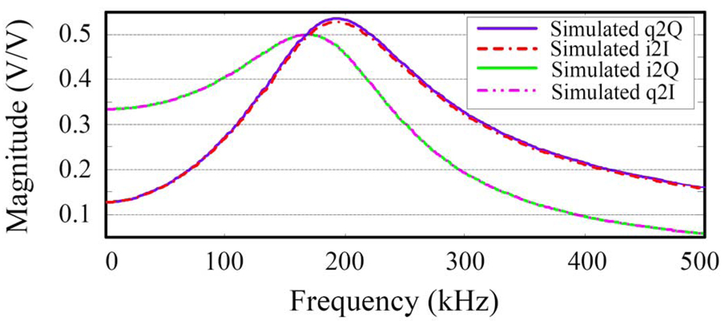
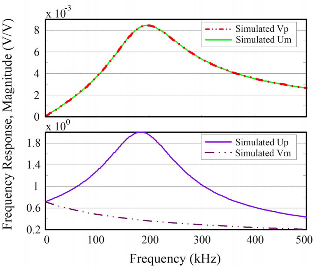
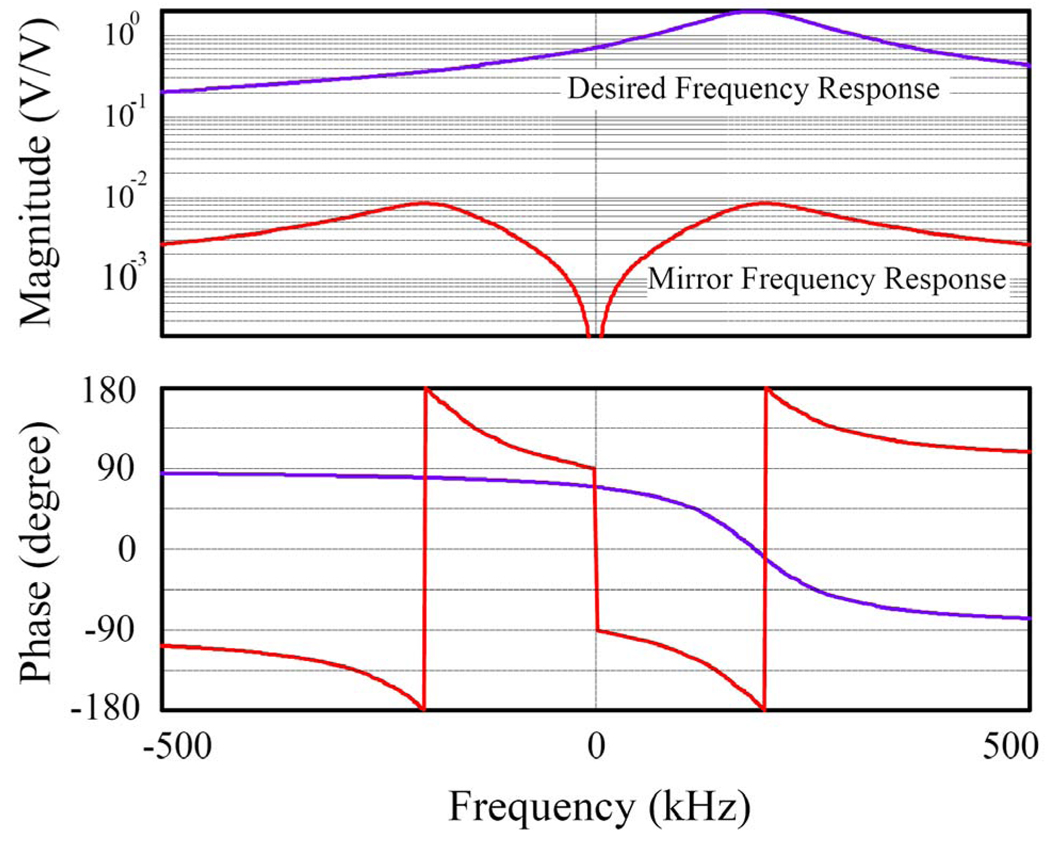
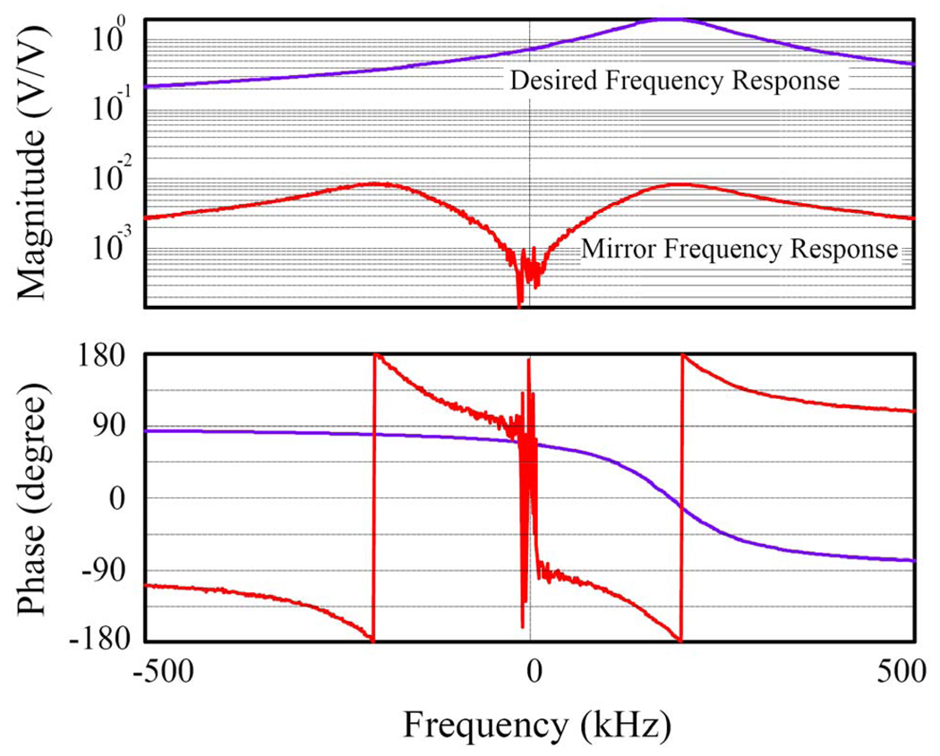
which tells us that the polyphase amplifier with a small capacitive mismatch has a desired response very close to that of the perfect amplifier, however its mirror response is not null anymore; moreover, since ε[Vp] is the complex conjugate of ε[Um], the mirror response has even amplitude and odd phase. This conclusion is validated by both simulations and experiments; as an example, the simulated response of the polyphase amplifier with a capacitive mismatch of 0.85% (shown in Fig. 7, Fig. 8, and Fig. 9) will be discussed later, in comparison with the results of our experiments.
Fig. 7.
Simulated transfer functions, 0.85% capacitor matching.
Fig. 8.
Simulated desired components Up, Vm (bottom) and mirror components Um, Vp (top) of frequency response, 0.85% capacitor matching.
Fig. 9.
Simulated amplitude (top) and phase (bottom) of overall polyphase desired and mirror frequency responses, 0.85% capacitor matching.
V. METHODS
A. Polyphase Amplifiers
To validate the mathematical model described above and to demonstrate that discrete polyphase amplifiers can have the performance required to be used as components of Cartesian feedback systems, we also designed and built a PCB hosting a polyphase amplifier that can be driven in one of three different ways:
-
--
with four single-ended independent inputs
-
--
with two fully-differential independent inputs
-
--
with two independent (positive) inputs, the other two (negative) inputs being AC grounded
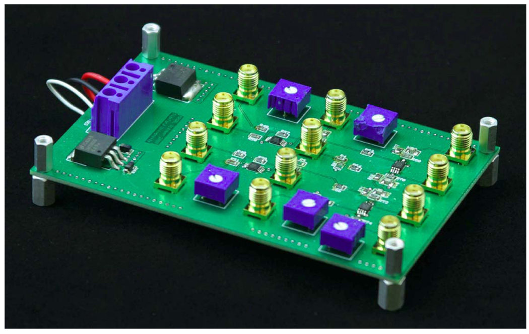
A picture of this board is shown in Fig. 4. The board allows bench testing of polyphase amplifiers built using discrete passive components of known tolerance and discrete fully-differential amplifiers of known (nominal) GBP.
Fig. 4.
PCB of polyphase amplifiers for bench validation of mathematical modeling.
B. Frequency Offset Cartesian Feedback
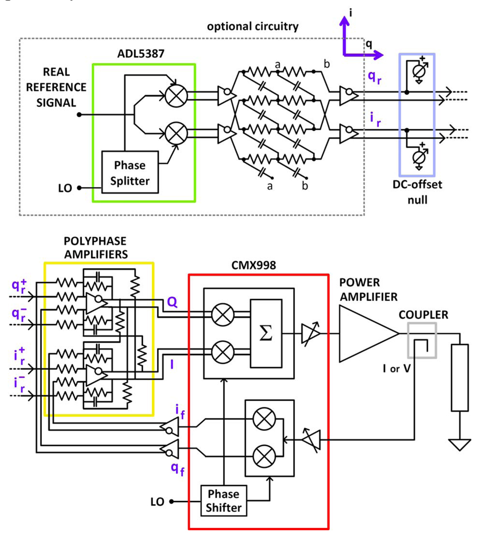
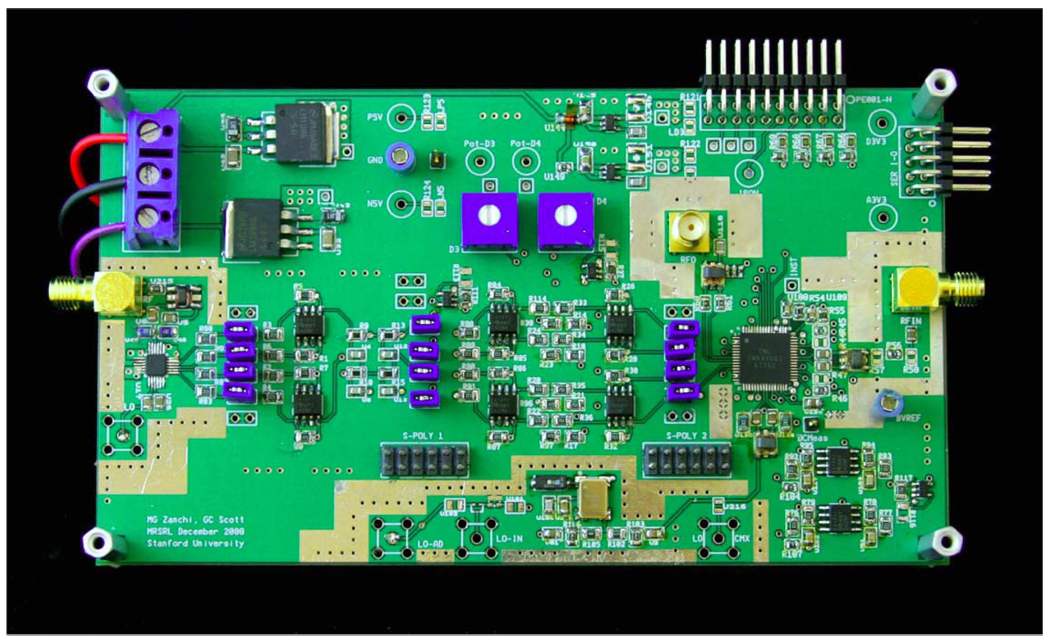
To demonstrate the feasibility of frequency-offset Cartesian feedback methods based on polyphase amplifiers, we then designed a PCB FOCF transmitter. A simplified block diagram and a picture of this frequency-offset Cartesian feedback transmitter are shown in Fig. 5 and Fig. 6, respectively.
Fig. 5.
Simplified block diagram of frequency-offset Cartesian feedback transmitter.
Fig. 6.
PCB of frequency-offset Cartesian feedback transmitter.
The transmitter includes all the essential blocks to control an external power amplifier (with the sole exception of the coupler that samples the power amplifier output voltage or current): an image-reject baseband reference down-converter that consists of ADL5387 broadband quadrature I/Q demodulator by Analog Devices followed by a passive polyphase filter with pole frequencies at 495 kHz and 520 kHz; polyphase difference amplifiers with 0.1% capacitor mismatch; CMX998 transmitter by CML Microcircuits of which we are currently using only the up-mixer, down-mixer and phase shifter; circuitry to manage the DC- or AC-coupling of the feedback signals (both approaches are possible); circuitry to convert the single-ended feedback signals from the down-mixer to differential; a ECS-UPO-5X7 programmable local oscillator by ECS Inc.; linear regulators. Digital serial control is provided for: (a) adjusting the loop phase, (b) enabling the up-mixer and down-mixer, and (c) selecting the up-mixer and down-mixer gains. Manual control with on-board trimmers is provided for adjusting the I, Q DC-offsets.
VI. EXPERIMENTS
A. Polyphase Amplifiers
The experiments described below were obtained by driving the polyphase amplifiers with four single-ended independent inputs (i+, i−, q+, q−) and measuring the four single-ended outputs elicited by each input (I+, I−, Q+, Q−). Appropriately combining these 16 measurements allows one to obtain the transfer functions i2I, i2Q, q2I and q2Q, the output components Up, Um, Vp, and Vm, and their combination into the overall desired and undesired responses.
B. Frequency Offset Cartesian Feedback
1) Open Loop Behavior
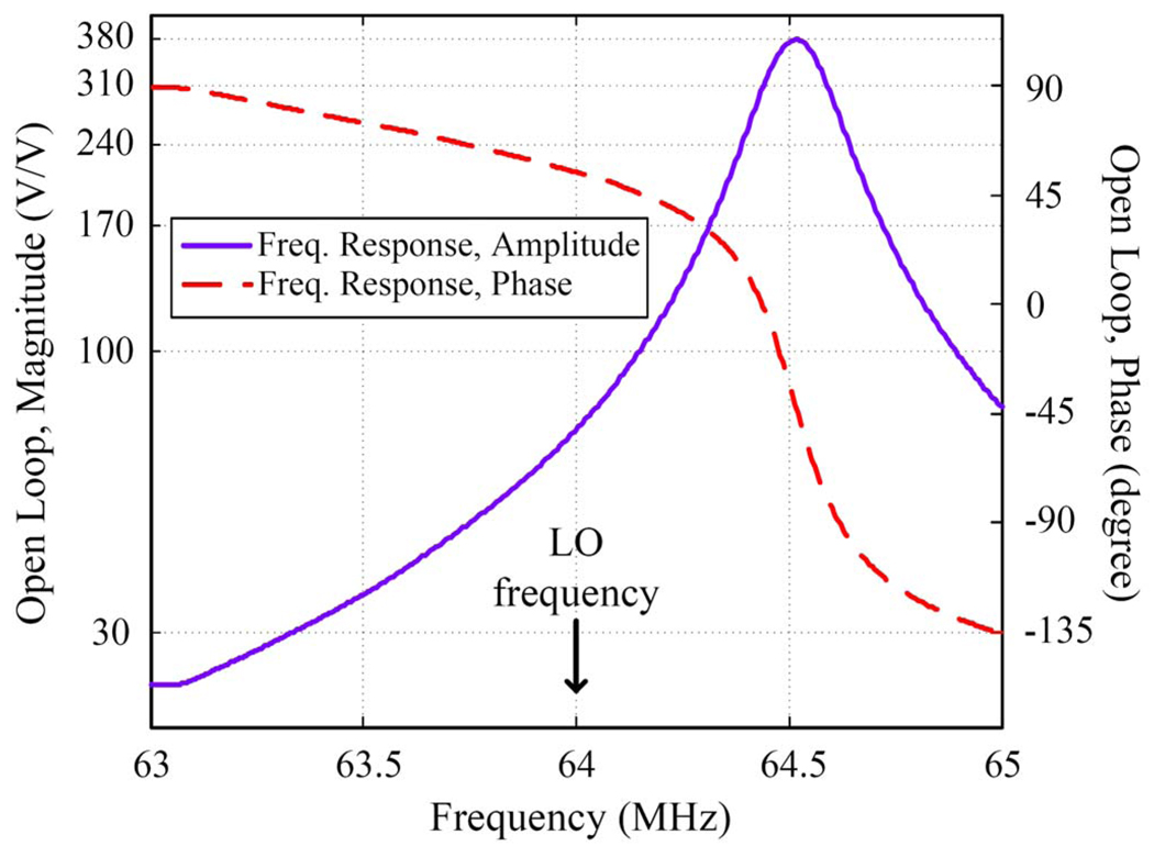
The first fundamental test was to characterize the open loop behavior of the frequency-offset Cartesian feedback system. Here we drove the RF down-mixer input of the CMX998 with a 2 MHz sweep, centered at 64 MHz (the local oscillator frequency), from a Network Analyzer (HP 3589A). The down-converted signal, first converted from single-ended to differential, was compared by the polyphase amplifiers to a null reference baseband signal and amplified. The output of the polyphase baseband amplifier was up-converted by the CMX998 and drove a 200 W, 53 dB gain power amplifier. The input of the Network Analyzer was the sampled output voltage of the power amplifier with a 50 ohm dummy load. The sample was obtained using a custom-built coupler with 30 dB attenuation. Using a microcontroller serial port interface (e.g. CML Microcircuits PE0001 card and GUI) (or, an Atmel AVR and Matlab interface), we were able to change the CMX998 integrated attenuators and phase shift, thus changing both amplitude and phase of the loop gain.
2) Closed Loop Image Rejection Performance
The second test demonstrated closed-loop control of a 300 W, power amplifier. This experiment consisted of two steps. In the first step we replicated the previous experiment to measure the phase shift value necessary for system stability; this time though, we used a 500 kHz sweep at the up-converted center frequency of the polyphase difference amplifiers (64.5 MH) to drive the RF down-mixer input of the CMX998. The LO frequency was still 64 MHz. In the second step, we set the value of phase shift found previously in the CMX998 registers, and closed the loop. We drove the reference down-converter input with a single-tone signal at the desired frequency 64.5+Δf MHz, first, and then the mirror frequency 63.5−Δf MHz, where Δf was equal to +/−50 kHz, +/−100 kHz, and +/−150 kHz. For each pair of desired and mirror frequencies (64.5+Δf MHz and 63.5−Δf MHz), we measured the mirror rejection. By doing so, we quantified the ability of the frequency-offset architecture to suppress the sideband signals created by the amplitude and phase mismatches of the mixers.
3) Two-Tone Tests
In a third experiment, two-tone tests were performed to measure the ability of both FOCF and classic CF to linearize a 200 W, 60 dB gain custom-made power amplifier. For FOCF, LO was 64 MHz, and the RF control band was centered at 64.465 MHz. To convert from FOCF to CF, we simply removed the four cross-coupling resistors (labeled RC in Fig. 2) of the polyphase amplifier causing the RF control band to overlap the LO at 64 MHz. In each case, we first drove the power amplifier directly using a two-tone signal (each tone offset 10 kHz from the respective center frequency of the RF control band). Next, we included the FOCF or CF-configured feedback system, and drove the reference down-converter inputs such that the power amplifier two-tone output levels approximately matched the prior levels. For all cases, we acquired spectra of the power amplifier output in a 120 kHz span centered at the respective RF control bandwidth. Two-tone generation and reception were performed by a custom digital transceiver system [22].
4) QAM Constellation
Finally, as a second linearity demonstration, we generated QAM constellation diagrams with 81 symbols using both the FOCF and classic CF configurations. The reference carrier was 64.5 (FOCF) and 64.0 (CF) respectively. Symbols were generated on a square grid by amplitude and phase modulation of the reference. Each system used similar 200 W, 60 dB gain power amplifiers driving a 50 Ω dummy load. For each configuration, we first acquired QAM plots by driving the power amplifier directly to similar power levels and onset of gain compression. We then added the FOCF or CF system, and collected linearized QAM data.
VII. RESULTS
A. Polyphase Amplifiers
We measured the response of our discrete polyphase amplifiers on the bench for different values of capacitive matching as well as at different values of the center frequency of the polyphase passband, and compared these measurements to the results of simulations obtained using the mathematical model described in the previous sections.
In a first experiment, we chose the components of our discrete polyphase circuit to obtain 0.85% mismatch dC/C of the capacitors, peak gain of 40 dB, and center frequency of nearly 200 kHz. We first chose the Linear Technology LT1994 fully differential discrete operational amplifiers whose gain-bandwidth product (GBP) of 70 MHz makes it possible to accurately implement the desired amplitude and shape of the polyphase passband. The passive resistors had 0.01% matching, obtained after measuring and cherry picking from a batch of 0.1% resistors. The simulated transfer functions and output response were calculated using our model with a 0.85% mismatch dC/C between capacitors and the same values of peak gain and center frequency. The normalized results of these simulations were compared with the normalized results of the experiments.
Fig. 7 shows the simulated magnitude transfer functions i2Q, i2I, q2I, q2Q while Fig. 8 show the simulated desired response (bottom, Up and Vm) and the simulated undesired response (top, Vp and Um). In these plots, the negative frequencies are folded in with the positive frequencies.
We then construct from Up, Vm, and Um, Vp the complete amplitude and phase for the desired and mirror responses as shown in Fig. 9 over negative and positive frequencies. Fig. 10 shows the experimental amplitude and phase response, created by the same construction procedure. The measured functions i2Q, i2I, q2I, q2Q and measured responses Up, Vm, Vp, Um that we used to obtain Fig. 10 are not shown as they were virtually indistinguishable from their respective simulations. This is evident in the comparison of Fig. 9 and Fig. 10 and demonstrates the validity of the model. Both model and measurement show that a 0.85% capacitor matching provides about 47 dB sideband rejection.
Fig. 10.
Measured amplitude and phase of overall polyphase desired and mirror frequency responses, 0.85% capacitor matching.
We also conducted experiments with capacitor matching between 0.05% and 0.1% and center frequencies up to 1.65 MHz. Though discrete capacitors with such low tolerances are not commercially available, the results of these experiments show the performance that could be achieved in an integrated or discrete version of the same circuits as technology improves and tolerances lower than 1% become available. At center offset frequencies over 650 kHz, we substituted the LT1994 (GBP 70 MHz) by Linear with THS4141 (GBP 200 MHz) by Texas Instruments, to faithfully reproduce the desired amplitude and shape of the polyphase passband. The peak gain was again equal to 100, the resistor matching to 0.01%. All of our experiments validate our model. The results of some of these experiments are summarized in Table I, and compared to the results of the simulations.
TABLE I.
Simulated and Measured Sideband Rejection at Different Center Frequencies of the Polyphase Pass Band
| Capacitor Mismatch [%] |
Center Frequency [kHz] |
Simulated Sideband Rejection [dB] |
Measured Sideband Rejection [dB] |
|---|---|---|---|
| 0.065 | 158 | 69.76 | 68.52 |
| 0.050 | 640 | 72.04 | 74.43 |
| 0.100 | 1490 | 66.02 | 65.19 |
Simulated and measured sideband rejection obtained with 0.05% C and 0.01% R at several values of the center frequency of the polyphase amplifier desired frequency response.
B. Frequency Offset Cartesian Feedback
1) Open Loop Behavior
As measured during our first experiment, Fig. 11 shows the amplitude and phase of the DC-coupled open loop gain of the Cartesian Feedback transmitter at full value of the CMX998 integrated gain and null phase shift. The peak gain amplitude is 377 at a frequency of 64.5 MHz. The integrated attenuators of the CMX998 can be controlled to decrease this value by 59 dB, of which 29 dB is in the feedback path (down-mixer) and 30 dB is in the forward path (up-mixer). Mostly the polyphase amplifiers are responsible for shaping the phase characteristics of the loop, which is characterized by a well-behaved 90° phase swing in a nearly 200 kHz bandwidth near the peak gain frequency, as well as by a rate of change of the gain amplitude near this frequency equal to −20 dB/decade. In our FOCF PCB transmitter, the DC biasing of the quadrature feedback signals at the input of the polyphase difference amplifier is set by appropriate independent circuitry including high-precision trimmers.
Fig. 11.
Amplitude and phase of the measured open loop gain of the Cartesian Feedback transmitter at full value of the CMX998 integrated gain.
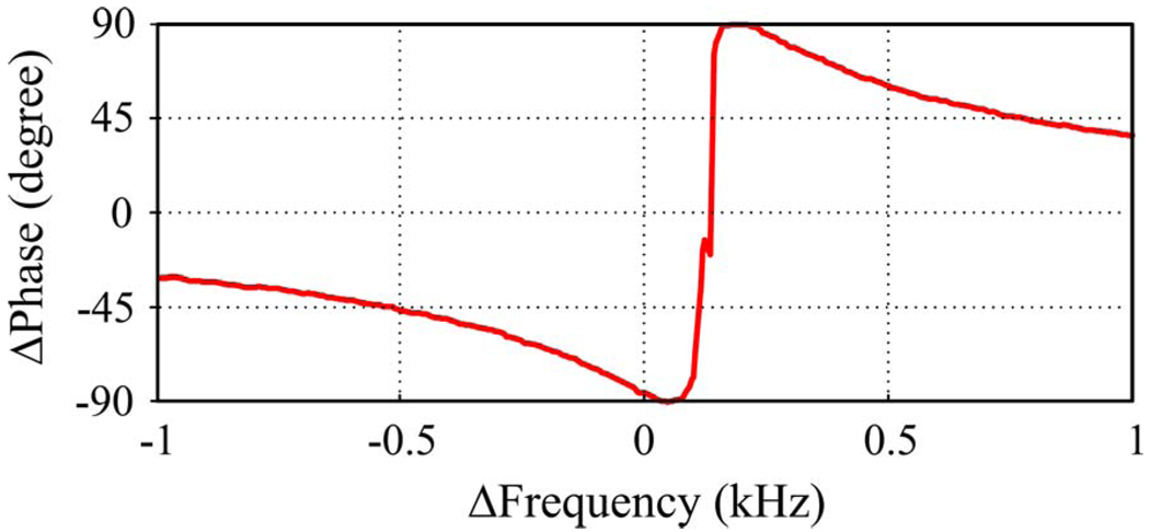
AC-coupling of the quadrature feedback path (after the down-conversion) is also possible to eliminate altogether the effect of the down-mixer’s DC-offsets. While this approach does offer advantages in some applications, for example when very high rejection of LO leakage is desirable, it also includes risks for the stability of the closed loop. Fig. 12 shows a close-up of the phase of the AC-coupled open loop gain of the FOCF transmitter. Because of the AC-coupling capacitors, a 180° roll-over occurs at the LO frequency. This phase behavior may create the conditions for instability at this frequency and thus prevent the loop operation.
Fig. 12.
Close-up of the AC-coupled open loop phase behavior near 64 MHz showing the 180 deg phase roll-over due to the AC-coupling capacitors.
2) Closed Loop Image Rejection Performance
Table II shows the lower sideband rejection measured with the closed-loop system in a 400 kHz span at the center frequency of the polyphase difference amplifiers (64.5 MHz). The sideband rejection of the closed-loop FOCF system is maximum at 64.5 MHz and is close to the sideband rejection of the polyphase difference amplifiers, as measured in previous experiments.
TABLE II.
Measured Sideband Rejection of the Closed Loop FOCF System
| Desired Frequency [kHz] |
Mirror Frequency [MHz] |
Measured Rejection [dB] |
|---|---|---|
| 64.35 | 63.65 | 40.94 |
| 64.40 | 63.60 | 48.82 |
| 64.45 | 63.55 | 57.49 |
| 64.50 | 63.50 | 61.16 |
| 64.55 | 63.45 | 58.64 |
| 64.60 | 63.40 | 56.84 |
| 64.65 | 63.35 | 55.10 |
Measured sideband rejection of the closed-loop FOCF system controlling a RF power amplifier near the center frequency of the polyphase control band.
The difference between the values in Table II and Table I, and the fact that the sideband rejection decreases more rapidly at frequencies lower than 64.5 MHz, results from image (negative frequency) generation by the error and reference input quadrature down-converters, which are then amplified unequally by the desired polyphase response to negative input frequencies. In this manner, besides mismatches in the quadrature up-converter, image rejection limits by quadrature down-conversion can translate to sideband generation.
3) Two-Tone Tests
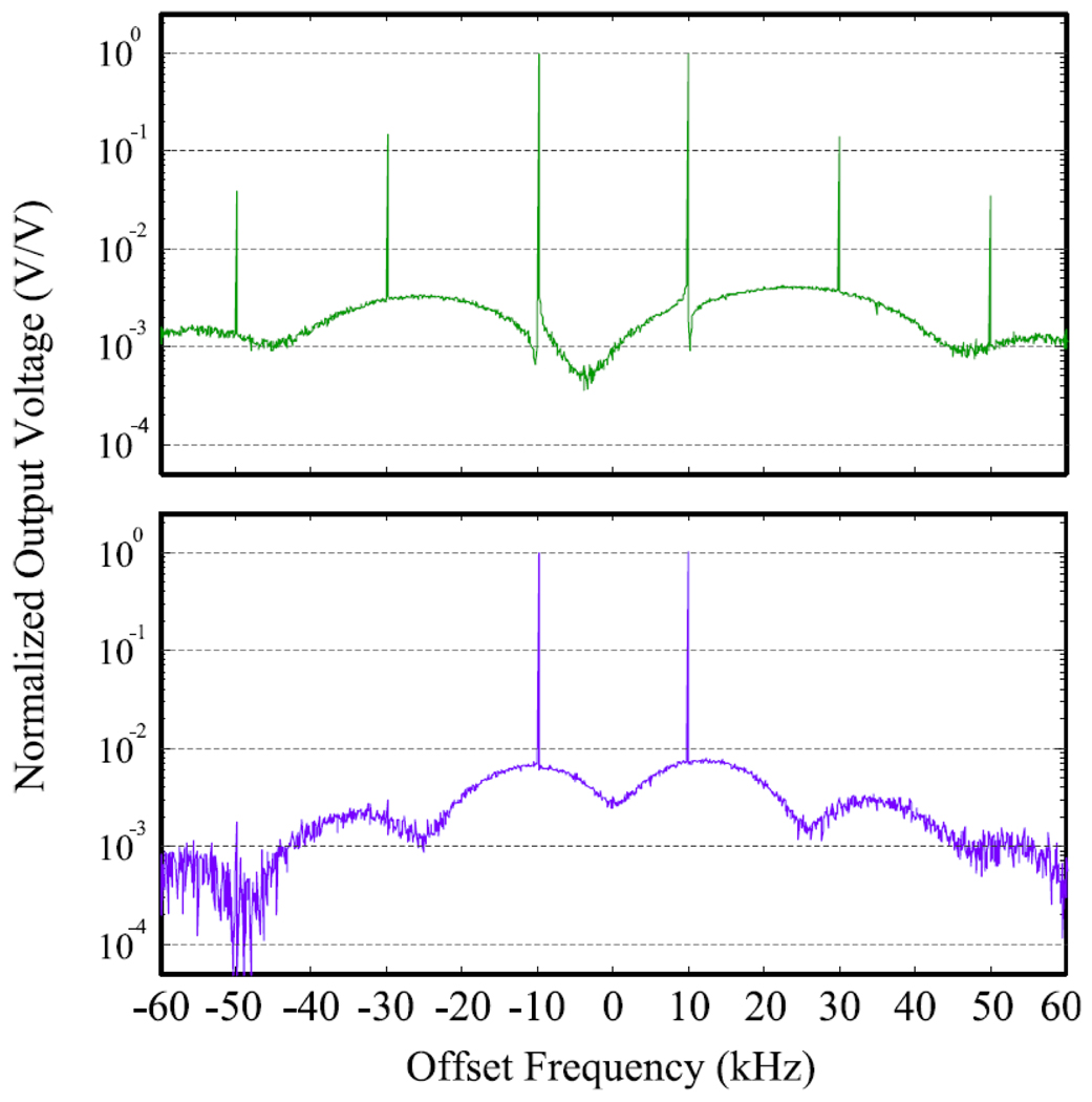
Fig. 13 (top) shows the power amplifier output spectrum when driven directly by two tones at 64.455 MHz and 64.475 MHz (these match the +10 kHz and −10 kHz offset from the FOCF RF control center frequency of 64.465 MHz). Fig. 13 (bottom) shows the power amplifier output spectrum after addition of the FOCF closed loop control. Here the distortion products are attenuated down to the noise level. Some increase in noise level is also apparent with closed-loop operation, especially near the main tones. This arose because of signal level and attenuation requirements for using the CMX998. Future designs of the FOCF transmitter will address this limitation, and optimization strategies are available since the noise analysis of a FOCF system should be equivalent to the noise analysis of a classic CF loop [1].
Fig. 13.
(Top:) Measured power amplifier output spectrum when directly driven by two tones offset +/−10 kHz from 64.465 MHz. (Bottom:) Measured two-tone output spectrum using the frequency-offset CF transmitter. The distortion products are attenuated down to the noise-level.
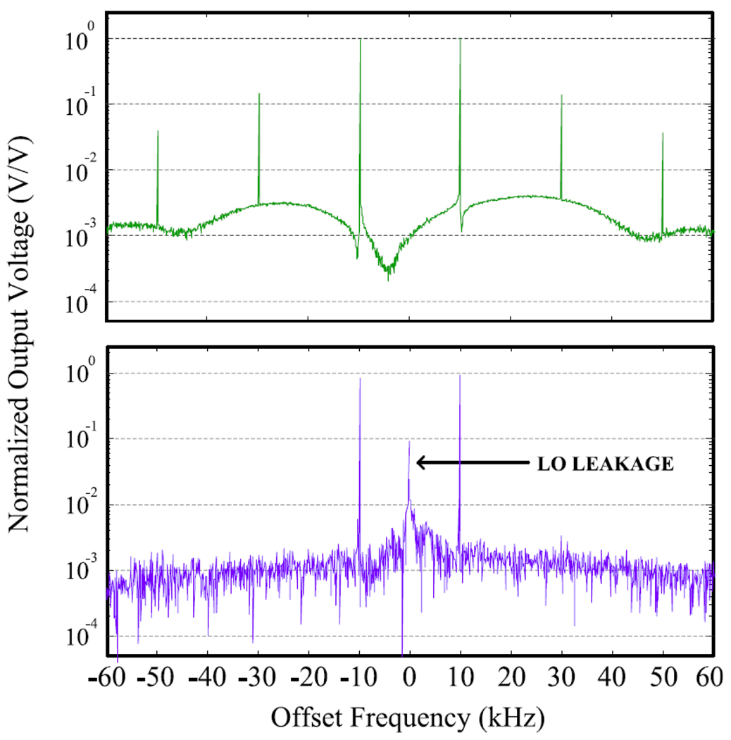
The two-tone distortion results are repeated in Fig. 14 for the classic CF configuration. Fig. 14 (top) shows the output spectrum of the power amplifier when directly driven by two tones at 64.01 MHz and 63.99 MHz (these tones are +10 kHz and −10 kHz offset from the classic CF LO and control center frequency of 64 MHz). Fig. 14 (bottom) shows the output spectrum of the power amplifier when controlled by the classic CF transmitter configuration. The classic CF system reduces the distortion products down to the noise level, just as the FOCF system does, but some LO-leakage and LO-noise is evident. More precise trimming of DC-offsets would have suppressed this effect. The FOCF system is immune to this effect, because the loop error amplification takes place at a low IF. Instead, the classic CF system is not: the loop error amplification band includes DC, where LO-leakage and DC-offset now create the undesirable “spike” at the center of the control bandwidth in Fig. 14.
Fig. 14.
(Top:) Measured power amplifier output spectrum when directly driven by two tones at 64 MHz +/−10 kHz. (Bottom:) Measured two-tone output spectrum using the classic CF-configured transmitter. The distortion products are attenuated down to the noise-level, but some LO-leakage and noise remain.
4) QAM Constellation
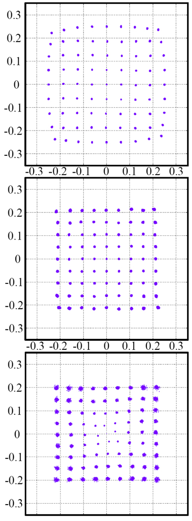
Fig. 15 (top) shows the QAM constellation of the directly-driven power amplifier with 64.5 MHz symbols, where gain compression effects are evident at the highest carrier amplitudes. This amplifier was then linearized by FOCF. The FOCF QAM grid is shown in Fig. 15 (middle), where gain compression effects have been removed. A second amplifier driven to similar gain compression levels (QAM grid not shown) was linearized by classic CF configuration. In Fig. 15 (bottom), the resulting QAM constellation of 64 MHz symbols (matching the CF LO) also shows linearization of high power symbols, but low power symbols suffer from DC/LO leakage and quadrature errors within the CF loop. Moreover, since the reference down-converter image reject filter was ineffective at DC, the down-converter quadrature and LO leakage errors also distort the baseband reference signals, prior to the CF loop. Higher noise levels at baseband are again evident.
Fig. 15.
Measured QAM constellation with: 200 W power amplifier only (top), closed loop FOCF (center), and closed loop classic CF (bottom).
VIII. DISCUSSION
In the FOCF system, quadrature errors result in different image frequency distributions compared to classic Cartesian feedback. Up(ω) and Vm(−ω) together form the ideal response of the polyphase amplifier, in this case, a positively shifted single pole system, as described by (5) and shown for ωc = 200 kHz in Fig. 5. In the ideal response, the input and output frequencies have the same sign.
Assume the positive-frequency input signals within some Δω of the pole frequency to be within the control passband. The negative-frequency response, Vm, is instead assumed to be well outside the control bandwidth, leading to an attenuation of −20 dB/decade for increasing negative input frequencies. Under Cartesian closed loop conditions, the passband gain will be set by the feedback factor and not Up, but negative input frequency gain will still be proportional to Vm. The relative closed loop gains at +/− ω define image rejection and will determine the ability of the Cartesian loop to reject image frequencies (in this case negative) generated elsewhere in the system. The closed loop image rejection will be less than the polyphase response ratio of Vm and Up.
Vp(ω) and Um(−ω) together describe the overall mirror response of the polyphase amplifier and are null in ideal polyphase architectures. In real architectures, they are undesired since they create an output frequency of opposite sign to the input frequency. While the Vp output frequencies are outside the control bandwidth, the Um output frequencies can fall within the control bandwidth where they are indistinguishable from the desired output signal Up. However, this latter case would require the deliberate injection of a large negative frequency signal, which is not assumed here.
The ability of the amplifiers to minimize the mirror response is thus an important figure of merit. The existence of any negative frequency, ω− at the quadrature up-converter input generates an undesired lower sideband output at ωo-ω−. We define sideband rejection of the polyphase amplifiers as the ratio Vp / Up. This ratio represents the negative frequency output amplitude per unit amplitude positive input frequency. Mismatches in the quadrature up-converter stage would likewise create a lower sideband response. Finally, negative (image) frequencies generated by an imperfect quadrature down-converter in the Cartesian loop, will be somewhat attenuated by the desired closed loop polyphase response, but yet again will lead to lower sideband generation.
In general higher frequency offsets should improve the image attenuation. Moreover, for some applications of the FOCF method, it may be desirable to move the mirror frequency band away from the LO frequency by a certain minimum. For example, in MRI, the complex baseband response of the FOCF system reduces the system requirements in terms of mismatches and DC-offsets necessary to obtain an artifact-free MR image when the baseband passband center frequency of the polyphase architecture is high enough so that the mirror frequency band is outside the MRI spin excitation bandwidth. There are, however, limits to the maximum value of the baseband passband center frequency that can be obtained. One of these limits is the finite gain-bandwidth product of the amplifiers implementing the loop driver polyphase amplifiers. The analysis of the effects that the gain-bandwidth product has on desired transfer function is presented in the Appendix to this paper, and it provides the designer of polyphase amplifiers a tool to select the fully differential amplifiers with the necessary performance in terms of gain and bandwidth. As a rule of thumb, a gain-bandwidth product higher than 500 times the desired passband (IF) center frequency is required.
A key consideration is stability and bandwidth. Since FOCF differs from classic CF only in the LO not overlapping the control band, gain K and bandwidth ωo selection criteria are otherwise identical. In both cases, the phase shift over the RF unity-gain open loop bandwidth must not reach +/−180 degrees. Any extra source of time or group delay inside the control loop will constrain the feasible bandwidth. Without extra phase compensation, the error amplifiers can contribute a total 180° degree phase variation; thus, instability will occur if an equal variation occurs elsewhere in the loop, making the sum of the two variations equal to 360°. Usually a 45° degree phase margin is desirable at each band edge, making only an additional 90° total variation acceptable. The group delay responsible for a phase variation of ΔΦ degrees in bandwidth B, in Hz, is simply τ=ΔΦ/360B. For example, for 5 MHz bandwidth and 45° degree phase margin, a group delay of only 50 ns can be tolerated. This is equivalent to the time delay of a 10 m RG58A/U coax cable. Clearly, the use of devices with high group delay within the loop is not advisable, as it would limit the achievable bandwidth significantly. A 150 MHz, 1.5 MHz bandwidth surface acoustic wave (SAW) filter can easily add 2.5 µs delay (e.g. model 819-IF150.0M-B, Oscilent Corporation). This filter would limit the achievable system bandwidth (with 45° degree phase margin) to 100 kHz, if all other group delay sources within the loop were negligible.
The relationship between the quadrature reference signals (ir, qr in Figure 1) is critical, since the polyphase loop error amplifier selectively amplifies the complex reference signal (ir, qr) characterized by a +90° phase relationship representing positive frequency signals.. The FOCF control system operates somewhat like single sideband (SSB) modulation. However, the FOCF approach still allows the same modulation bandwidth control as classic Cartesian feedback. The Frequency-Offset Cartesian feedback system has exactly the same loop error frequency response, only shifted to a positive (or, negative) frequency. In both scenarios, the information that can be sent to the antenna is the same.
IX. CONCLUSION
We have introduced a new frequency-offset Cartesian feedback method (based on polyphase difference amplifiers) to control RF power amplifiers that significantly reduces the requirements in terms of quadrature errors and DC-offset of the classic Cartesian feedback linearization method.
We have derived a mathematical model to separate and describe the desired and undesired response of the polyphase amplifiers to both positive and negative frequencies. We have validated the accuracy of our model with experimental testing of a printed-circuit board design based on fully-differential amplifiers and analog components, and demonstrated that polyphase difference amplifiers—even with discrete implementations—can achieve up to 70 dB rejection of the mirror frequencies created by quadrature errors of the down-mixers in Cartesian feedback loop.
Furthermore, we have demonstrated the feasibility of frequency-offset Cartesian feedback control of RF power amplifiers using a transmitter based on a printed circuit board design. In stable closed-loop conditions, the frequency-offset Cartesian feedback system shows up to 60 dB sideband rejection, in addition to the excellent power amplifier linearization properties of the classic Cartesian feedback architecture.
ACKNOWLEDGMENT
The authors would like to thank Prof. Thomas Lee at the Stanford Microwave Integrated Circuits Laboratory, Stanford University, CA for his valuable comments on our research.
This work was supported in part by the grants: NIH R01EB008108, R33CA118276, and R21EB007715.
Biographies

Marta G. Zanchi received the B.S. degree in biomedical engineering and the M.S. degree in electrical engineering from Politecnico Di Milano, Italy, in 2003 and 2005, respectively.
She received the Politecnico Di Milano highest student honor in 2006. She holds a certificate in entrepreneurship and an award from the Stanford Graduate School of Business, Stanford, CA.
Since May 2006, she is studying a Ph.D. in magnetic resonance imaging at Stanford University, Stanford, California, USA.

John M. Pauly received the PhD degrees in electrical engineering at Stanford University, California, USA in 1989. He is a Professor of electrical engineering at Stanford University. His main research interests are in MRI, and the use of MRI for guiding minimally invasive interventional procedures.
He teaches classes in image reconstruction for medical imaging, as well as RF pulse design for MRI at Stanford. He holds 42 U.S. patents and has authored and co-authored 110 journal articles.
Dr. Pauly is a Member of the IEEE and is Associate Editor of IEEE Transactions on Medical Imaging.

Greig C. Scott received the BASc (Honours) degree in electrical engineering from the University of Waterloo in 1986, and the MASc and PhD degrees in electrical engineering at the University of Toronto, Canada in 1989 and 1993 respectively.
He is a Sr. Research Engineer with the magnetic resonance systems research lab (MRSRL) in electrical engineering at Stanford University, and has served as a consultant to several interventional device companies. His main research interests are MRI instrumentation, and electromagnetic imaging techniques for RF safety and MR-guided therapy.
APPENDIX
A. Effect of the limited GBP of fully differential amplifiers to the effective transfer function of a polyphase architecture
To derive the effective transfer function He(ω) of the polyphase architecture employing fully-differential (FD) amplifiers with finite gain-bandwidth product (and perfectly matched components), we describe each FD amplifier with analog behavior characterized by finite DC gain, A, and finite bandwidth defined by the frequency of a single pole, ωp; the transfer function of this behavior is shown in (29). The gain-bandwidth product (GBP) is, by definition, given by the product of A and ωp.
| (29) |
We then solve the linear equation for the outputs Q, I as a function of the inputs q, i. Solving this equation, we define two new quantities, the magnitude factor M(ω) and shift factor S:
| (30) |
| (31) |
The effective transfer function He(ω) of the polyphase architecture employing FD amplifier with finite GBP is:
| (32) |
Where we introduce the effective passband center frequency ωec = ωc·S−1, effective half passband width ωeo = ωo·M·S−1, and effective peak gain Ke = K·M−1.
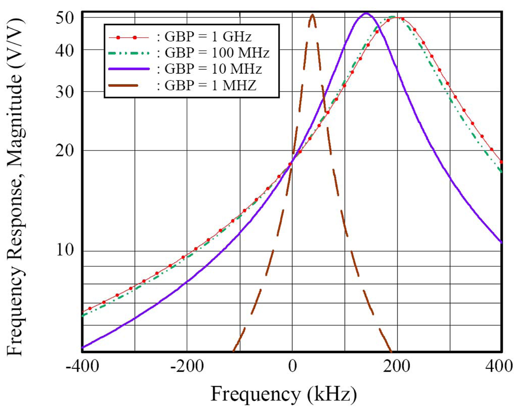
Fig. 15 shows the amplitude of the effective transfer function of a polyphase architecture of desired passband center frequency 200 kHz, desired half passband width 80 kHz, and desired peak gain 50, as a function of the GBP of the FD amplifiers. Here the finite bandwidth of the FD amplifiers is fixed at 10 Hz (ωp = 20π rad/s) while A varies from 108 to 105, a range of values typical of commercially available discrete FD amplifiers. He(ω) in the case of GBP = 108 approximates the ideal transfer function very well.
Fig. 15.
Amplitude of the Effective Transfer Function He(f) calculated in MatLab for several value of the GBP. In this plot, the pole frequency is kept constant (10 Hz), while the DC gain varies (from 0.1 M to 100 M). The same plot was obtained by varying, instead, the pole frequency (from 0.01 Hz o 10 Hz), while the DC gain was kept constant (100 M), and it is virtually identical in appearance to the plot shown here.
Almost identical plots can be obtained by varying the pole frequency of the FD amplifiers (from 10 to 0.01 Hz) while A is fixed (A equal to 108). This result illustrates one of the key findings of this analysis: given the desired transfer function and the chosen FD amplifiers, and considering that ωp is typically small (less than 500 Hz) compared to ωo and ωc, then the effective transfer function is almost entirely determined by the product GBP, not by A and ωp independently.
Contributor Information
Marta G. Zanchi, Electrical Engineering Department, Stanford University, Stanford, CA 94305 USA. (phone: 650-723-1904; fax: 650-723-8473; mgzanchi@stanford.edu)..
John M. Pauly, Electrical Engineering Department, Stanford University, Stanford, CA 94305 USA. (phone: 650-723-4569; fax: 650-723-8473; pauly@stanford.edu)..
Greig C. Scott, Electrical Engineering Department, Stanford University, Stanford, CA 94305 USA. (phone: 650-724-3639; fax: 650-723-8473; greig@mrsrl.stanford.edu)..
REFERENCES
- 1.Kenington P. High Linearity RF Amplifier Design. Norwood, MA: Artech House; 2000. [Google Scholar]
- 2.Crols J, Steyaert M. CMOS Wireless Transceiver Design. Norwell, MA: Kluwer Academic Publishers; 1997. [Google Scholar]
- 3.Zhu Y. Parallel excitation with an array of transmit coils. Magnetic Resonance in Medicine. 2004 Mar.vol. 51(issue 4):775–784. doi: 10.1002/mrm.20011. [DOI] [PubMed] [Google Scholar]
- 4.Hornak JP. The Basics of MRI: online technical book. 1996. http://www.cis.rit.edu/htbooks/mri/ [Google Scholar]
- 5.Petrovic V. VHF SSB Transmitter Employing Cartesian Feedback. Proceedings of the IEE Conference on Telecommunications, Radio and Information Technology; May 1984; Birmingham, UK. pp. 161–165. [Google Scholar]
- 6.Johansson M, Mattsson T. Transmitter linearization using Cartesian feedback for linear TDMA modulation. Proceedings of the 1991 IEEE 41st Vehicular Technology Conference; May 1991; St. Louis, Missouri (USA). pp. 439–444. [Google Scholar]
- 7.Johansson M, Mattsson T, Sundstrom L, Faulkner M. Linearization of multi-carrier power amplifiers. Proceedings of the 1993 IEEE 43rd Vehicular Technology Conference; May 1993; Seaucus, New Jersey (USA). pp. 684–687. [Google Scholar]
- 8.Johansson M, Sundstrom L. Linearisation of RF multicarrier amplifiers using Cartesian feedback. Electronics Letters. 1994 Jul.vol. 30-14:1110–1112. [Google Scholar]
- 9.Faulkner M, Contos D, Briffa M. Linearisation of power amplifiers using RF feedback. Electronics Letters. 1995 Nov.vol. 31(issue 23):2023–2024. [Google Scholar]
- 10.Boloorian M, McGeehan JP. Linearisation of frequency-hopped transmitters using Cartesian feedback. Proceedings of the 1995 IEEE 45th Vehicular Technology Conference; Jul. 1995; Chicago, Illinois (USA). pp. 520–524. [Google Scholar]
- 11.Boloorian M, McGeehan JP. Maximisation of Cartesian transmitter linearisation bandwidth. Electronics Letters. 1996 Sept.vol. 32(issue 19):1823–1824. [Google Scholar]
- 12.Briffa MA, Faulkner M. Stability analysis of Cartesian feedback linearisation for amplifiers with weak nonlinearities. IEEE Proceedings in Communications. 1996 Aug.vol. 143(issue 4):212–218. [Google Scholar]
- 13.Briffa MA, Faulkner M. Gain and Phase Margins of Cartesian Feedback RF Amplifier Linearisation. IREE Journal of Electrical and Electronics Engineering Australia. 1994 Dec.vol. 14(issue 4):283–283. [Google Scholar]
- 14.Briffa MA, Faulkner M. Stability considerations for dynamically biased Cartesian feedback linearization. Proceedings of the 1994 IEEE 44th Vehicular Technology Conference; Jun. 1994; Stockholm, Sweden. pp. 1321–1325. [Google Scholar]
- 15.Faulkner M, Contos D, Briffa M. Performance of automatic phase adjustment using supply current minimization in a RF feedback lineariser. Proceedings of the 1997 IEEE 8th International Symposium on Personal, Indoor and Mobile Radio Communications; Sept. 1997; Helsinki, Finland. pp. 858–862. [Google Scholar]
- 16.Faulkner M. Amplifier linearization using RF feedback and feed-forward techniques. IEEE Trans. Vehicular Technology. 1998 Feb.vol. 47(issue 1):209–215. [Google Scholar]
- 17.Dawson JL, Lee TH. Automatic phase alignment for a fully integrated Cartesian feedback power amplifier system. IEEE Journal of Solid-State Circuits. 2003 Dec.vol. 38(issue 12):2269–2279. [Google Scholar]
- 18.Dawson J, Lee TH. Feedback Linearization of RF Power Amplifiers. Norwell, MA: Kluwer Academic Publishers; 2004. [Google Scholar]
- 19.Hoult D, Foreman D, Kolansky G. Overcoming high-field RF problems with non-magnetic Cartesian feedback transceivers. Magnetic Resonance Materials in Physics, Biology and Medicine. 2008 Mar.vol. 21(issue 1–2):15–29. doi: 10.1007/s10334-007-0089-8. [DOI] [PubMed] [Google Scholar]
- 20.Hoult D, Kolansky G, Kripiakevich D. A 'Hi-Fi' Cartesian feedback spectrometer for precise quantitation and superior performance. Journal of Magnetic Resonance. 2004 Nov.vol. 171(issue 1):57–63. doi: 10.1016/j.jmr.2004.07.019. [DOI] [PubMed] [Google Scholar]
- 21.Hoult D, Kolansky G, Kripiakevich D, King SB. The NMR multi-transmit phased array: a Cartesian feedback approach. Journal of Magnetic Resonance. 2004 Nov.vol. 171(issue 1):64–70. doi: 10.1016/j.jmr.2004.07.020. [DOI] [PubMed] [Google Scholar]
- 22.Stang PP, Kerr A, Grisson W, Pauly JM, Scott GC. Vector Iteration Predistortion: an auto-calibration method for transmit arrays. presented at 17th International Society for Magnetic Resonance in medicine Scientific Meeting & Exhibition; Honolulu, Hawaii. 2009. [Google Scholar]
- 23.Marshall CB. Active Polyphase Filters. 4 723 318. U.S. Patent. 1988 Feb. 2
- 24.Crols J, Steyaert MSJ. Low-IF topologies for high-performance analog front ends of fully integrated receivers. IEEE Trans. on Circuits and Systems II: Analog and Digital Signal Processing. 1998 Mar.vol. 45(issue 3):269–282. [Google Scholar]
- 25.Linggajaya K, Seng JGYK. A new active polyphase filter for wideband image reject downconverter; Proceedings of the 2002 International Conference on Semiconductor Electronics; Penang, Malaysia: 2002. Dec., pp. 213–217. [Google Scholar]
- 26.Behbahani F, Kishigami Y, Leete J, Abidi AA. CMOS mixers and polyphase filters for large image rejection. IEEE Journal of Solid-State Circuits. 2001 Jun.vol. 36(issue 6):873–887. [Google Scholar]
- 27.Zanchi MG, Pauly JM, Scott GC. Frequency Offset Cartesian Feedback Control System for MRI Power Amplifier. presented at 17th International Society for Magnetic Resonance in medicine Scientific Meeting & Exhibition; Honolulu, Hawaii. 2009. [Google Scholar]


