Abstract
We demonstrate a technique in microscopy which extends the domain of atomic force microscopy to optical spectroscopy at the nanometer scale. We show that molecular resonance of feature sizes down to the single molecular level can be detected and imaged purely by mechanical detection of the force gradient between the interaction of the optically driven molecular dipole and its mirror image in a platinum coated scanning probe tip. This microscopy and spectroscopy technique is extendable to frequencies ranging from radio to infrared and the ultraviolet.
Atomic force microscopes (AFM) have been successfully applied to nanometer scale imaging of chemical,1 magnetic,2, 3 and electrostatic4, 5 properties of surfaces. These microscopes rely on probe tips (typically silicon) suitably modified to detect the specific property of interest and to translate it into a detectable force. However, except for the magnetic resonance force microscope6 which has been used to detect nuclear magnetic resonance at millikelvin temperatures, AFM based scanning force microscopes have been primarily used to study material properties on the nanometer scale and not for spectroscopic identification of the materials being investigated. The ability to apply AFM’s for nanometer scale spectroscopic analysis will open new opportunities in materials science and biology. In biology, it could be used to study molecular cell surface interactions or for next generation DNA sequencing technologies.
Our microscope is built around an attractive tapping mode AFM,7 where the cantilever is vibrated at its first mechanical resonance f0 (Fig. 1). We modulate the laser beam at a frequency, fm, which modulates the image force gradient between object features and their mirror images also at fm. This force gradient modulation in turn modulates the cantilever mechanical resonance frequency generating sidebands at f0+fm and f0−fm. The f0+fm sideband which is arranged to lie on top of the second mechanical resonance of the cantilever, is detected using a lock-in amplifier while the object is raster scanned to record the optical image. The reference for the lock-in is derived by mixing the f0 and fm drive signals in a double balanced mixer followed by a bandpass filter centered at f0+fm.
Figure 1.
Schematic of the image force microscopy experiment.
A 10 nm radius platinum coated silicon tip is illuminated by a laser beam using an oil immersion objective (NA=1.45) focused via a glass microscope cover slide. The focused laser excites an optical dipole moment within the object. As the tip approaches the object on the glass surface, this excited dipole sees its mirror image within the tip resulting in an attractive force and force gradient. To further enhance this dipole-dipole interaction, we use a radial polarizer (ARCoptix) at the entrance pupil of the objective. The optics is arranged so that we could independently couple up to four lasers (λ=633, 594, 543, 475 nm) into the objective. The optical power at the entrance pupil of the objective was adjusted to be 100 μW. We used a cantilever with stiffness constant k=3 n∕m and first mechanical resonance f0=65 kHz. We chose a laser modulation frequency fm=360 kHz and the frequency at the upper sideband f0+fm was detected at 425 kHz.
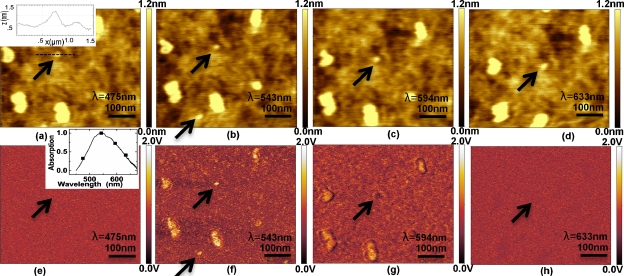
In the first experiment, we pipetted a 100 μL drop of 4×10⁻⁷ mM 6-tamra dye dissolved in water onto a clean glass microscope cover slide. The dye aggregated into tiny islands with an average dimension of approximately 50 nm while the smallest features (designated by arrows in Fig. 2) were on the order of 10 nm. We simultaneously recorded the topography (Fig. 2 top row) and the optical image force gradient (Fig. 2 bottom row) at a series of wavelengths around the optical resonance peak at 543 nm. As expected, aside form a slight thermal drift in the images, the topography signal shows no contrast variation with wavelength. The image force signal on the other hand shows a clear contrast variation as we scan through the optical resonance at 543 nm where the maximum contrast is observed. Virtually no contrast is visible in the optical image force micrographs at 475 and 633 nm. The optical image force micrographs were normalized so that the background signal was the same at all recorded wavelengths. The smallest optical image force feature recorded showing spectroscopic contrast was 10 nm in lateral dimensions and had a feature height of 0.5 nm [Fig. 2a inset], comparable to the height of a single 6-tamra molecule. Since the tip diameter was also approximately 10 nm, we infer that the smallest object feature must have a lateral dimension much smaller than 10 nm and is most probably a single molecule.
Figure 2.
6-tamra dye molecule images on glass as a function of wavelength: topography images [(a)–(d)]. Simultaneously recorded image force gradient images [(e)–(h)]. Inset in (a) line scan across a molecular feature. Inset in (e) spectral data points from image force microscope compared with bulk measurements from spectrometer.
To further validate our imaging concept, we spread a thick layer of 6-tamra dye onto a glass microscope cover slide and recorded an absorption spectrum using a Perkin Elmer Lambda 40 spectrophotometer. Figure 2e inset shows the optical image force gradient signal recorded on an island of 6-tamra as a function of wavelength superimposed on the recorded Perkin–Elmer spectrum (solid line); the agreement is excellent.
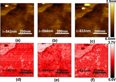
In a second series of experiments, we performed similar experiments to the 6-tamra experiments but using YOYO 3 dye (peak absorption near λ=594 nm). In this series of experiments, we were fortunate to trap a piece of debris within a YOYO 3 island. Figure 3 (first row) shows a series of topography images recorded at 543, 594, and 633 nm where the piece of debris in the center of the island is clearly visible. Figure 3 (second row) shows the simultaneously recorded optical image force gradient micrographs. The highest spectroscopic contrast is observed at λ=594 nm and as expected the debris particle shows no spectroscopic contrast.
Figure 3.
YOYO-3 dye molecule images on glass as a function of wavelength: topography images [(a)–(c)]. Simultaneously recorded image force gradient images [(d)–(f)].
There are four possible candidates for the observed optical contrast. The first two candidates derive from photodisplacement microscopy.8 In the first case, the tip enhanced optical field can lead to a highly localized light absorption within the molecules beneath the tip at their resonance frequency resulting in a temperature increase and a corresponding periodic dilation of the glass substrate at the chopping frequency fm. However, if this were the case, one would expect a dilation amplitude ΔL given by9 ΔL=Pabsα∕κ, where Pabs is the local absorbed power beneath the tip, α is the thermal expansion coefficient and κ is the thermal conductivity of the glass substrate. If we assume a single molecule under the tip with an absorption cross section σ=10−16 cm2 we get ΔL=6×10⁻¹⁸ m—too small to be detected using our setup. In the second case, the optical field can result in light absorption within the tip causing it to periodically dilate. We have both calculated and simulated this situation for our specific geometry of a platinum coated silicon tip with backside illumination and find that the resulting periodic dilation amplitude is less than 2.1×10⁻⁶ nm—too small to be detected by our system (see Ref. 10). The third candidate possibility results from the direct dilation of a molecule caused by the absorbed optical power. If we assume a rather high temperature increase of 10 K due to the molecular absorbed power and α=10−6∕K we estimate the dilation of a molecule to be on the order of 2×10⁻⁶ nm—again too small to be detected in our setup. The fourth contrast mechanism is the one proposed in this article, namely, the image force gradient between the object and its image dipole in the scanning probe tip.
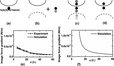
To get an estimate of the image force gradients involved, we performed a finite element (COMSOL) analysis of the tip sample interaction. The salient features of the physics can be understood by referring to Fig. 4a showing a tip interacting with a particle on a substrate. We can include the effect of the glass substrate by replacing it with the mirror image of the tip in the glass plus the mirror image of the particle in the glass—Fig. 4b; the complex reflectivity, R, of the glass mirror being given by the Fresnel equations R=(1−n)∕(1+n), n being the complex refractive index of glass. We then approximate the situation in Fig. 4b with Fig. 4c, where the particle∕image pair in Fig. 4b makes multiple reflections in the tip and in the (weak) tip mirror image. If we neglect the weak reflections, we can approximate the situation in Fig. 4c to first order with Fig. 4d where the particle is essentially interacting with its mirror image in the tip. Figure 4e—dotted line—shows the optical image force gradient versus tip—substrate spacing calculated using a full electromagnetic simulation of the situation in Fig. 4a (without the particle) compared with experimental approach curves obtained with the control loop momentarily opened; the detected signal was normalized with respect to the measured tip vibration amplitude at the first harmonic. The vibration amplitude of the cantilever with the tip retracted far from the sample surface was 40 nm. Figure 4f shows the calculated force gradient versus tip—particle spacing for the case of Fig. 4a with the particle in place. As expected, we see a rapid decay of the signal (over a distance of a nanometer) due to the highly localized image force dipole coupling. We also experimentally observe this rapid decay; the image contrast completely disappears when the tip is retracted just 1 nm from the surface (much like in a tunneling microscope) although so far it has been difficult to record this decay curve due to the thermal drift in the scanning system. A full electromagnetic field calculation and a simplified dipole theory calculation for the case of Figs. 4e, 4f is provided in Ref. 10.
Figure 4.
Experimental image force gradient approach curves compared with finite element (FE) simulations: simplified representation of dipole-tip-sample interactions [(a)–(d)]. Image force gradient on Pt tip approaching a glass substrate compared with FE simulations (solid line) (e). FE simulation of image force gradient on Pt tip approaching a 1 nm particle on a glass substrate (f).
We can estimate the image force and force gradient from the measured data. The S∕N ratio at the second resonance of 425 kHz was 30 dB in a bandwidth of 10 Hz. The Q at the second resonance Q1 was 115 and the Q at the fundamental Q2 was also 115. From this we calculate that the detected force was 2.7×10⁻¹² N and the force gradient was 2.1×10⁻⁵ N∕m (see Ref. 10). The detectable force can be reduced down to 10−18 N range by operating in vacuum and increasing Q to 10 000, by going to lower temperatures, by increasing cantilever resonance frequencies or by using lower stiffness cantilevers.6, 7
In conclusion, we introduced a new technique of scanning microscopy based on detecting the image force gradient between an object and its mirror image in a scanning probe tip. While apertureless near-field microscopes11, 12 based on light scattering from tips have had great success in imaging nanoscopic objects from the visible to the infrared, the signals are very weak because they are based on far-field detection of a near-field interaction. We believe that our approach can be extended from the rf though the visible and infrared wavelengths and we see no impediment to achieving atomic resolution at visible wavelengths with this technique. Furthermore, electronic and magnetic oscillations could also be imaged using the same technique.
Acknowledgments
This work was supported by NIH Grant Nos. HG-04431 and HG-04549 and NSF (Grant No. 0328162) sub award from UIUC Nano CEMMS Center. The Perkin-Elmer spectrum was recorded by Susana Sanchez at the Laboratory for Fluorescence Dynamics at the University of California, Irvine. Author contributions: H.K.W. came up with the idea and oversaw the entire project. I.R. set up and performed the experiments including the COMSOL simulations. K.U. provided help with the AFM image acquisition. H.K.W. wrote the paper.
References
- Frisbie C. D., Rozsynai L. F., Noy A., Wrighton M. S., and Lieber C. M., Science 265, 2071 (1994). 10.1126/science.265.5181.2071 [DOI] [PubMed] [Google Scholar]
- Martin Y. and Wickramasinghe H. K., Appl. Phys. Lett. 50, 1455 (1987). 10.1063/1.97800 [DOI] [Google Scholar]
- Rugar D., Mamin H. J., Guethner P., Lambert S. E., Stern J. E., McFadyen I., and Yogi T., J. Appl. Phys. 68, 1169 (1990). 10.1063/1.346713 [DOI] [Google Scholar]
- Martin Y., Abraham D. W., and Wickramasinghe H. K., Appl. Phys. Lett. 52, 1103 (1988). 10.1063/1.99224 [DOI] [Google Scholar]
- Nonnenmacher M., O’Boyle M. P., and Wickramasinghe H. K., Appl. Phys. Lett. 58, 2921 (1991). 10.1063/1.105227 [DOI] [Google Scholar]
- Rugar D., Yannoni C. S., and Sidles J. A., Nature (London) 360, 563 (1992). 10.1038/360563a0 [DOI] [Google Scholar]
- Martin Y., Williams C. C., and Wickramasinghe H. K., J. Appl. Phys. 61, 4723 (1987). 10.1063/1.338807 [DOI] [Google Scholar]
- Ameri S., Ash E. A., Neuman V., and Petts C. R., Electron. Lett. 17, 337 (1981). 10.1049/el:19810238 [DOI] [Google Scholar]
- Black E. D., Grudinin I. S., Rao S. R., and Libbrecht K. G., J. Appl. Phys. 95, 7655 (2004). 10.1063/1.1728312 [DOI] [Google Scholar]
- See supplementary material at http://dx.doi.org/10.1063/1.3480608 for full finite element electromagnetic and thermal simulations.
- Zenhausern F., Martin Y., and Wickramasinghe H. K., Science 269, 1083 (1995). 10.1126/science.269.5227.1083 [DOI] [PubMed] [Google Scholar]
- Knoll B. and Keilmann F., Nature (London) 399, 134 (1999). 10.1038/20154 [DOI] [Google Scholar]


