

Abstract
We present benchtop and in vivo experimental results from an integrated circuit designed for wireless implantable neural recording applications. The chip, which was fabricated in a commercially available 0.6-μm 2P3M BiCMOS process, contains 100 amplifiers, a 10-bit analog-to-digital converter (ADC), 100 threshold-based spike detectors, and a 902–928 MHz frequency-shift-keying (FSK) transmitter. Neural signals from a selected amplifier are sampled by the ADC at 15.7 kSps and telemetered over the FSK wireless data link. Power, clock, and command signals are sent to the chip wirelessly over a 2.765-MHz inductive (coil-to-coil) link. The chip is capable of operating with only two off-chip components: a power/command receiving coil and a 100-nF capacitor.
Index Terms: Brain–machine interface (BMI), low power, neural prosthetics, telemetry, wireless
I. Introduction
Progress in modern systems neuroscience relies on the ability to monitor and record electrical signals produced by neurons in the brain or peripheral nervous system. Despite advances in miniaturizing the electrodes used to detect neural activity, most modern electrophysiological studies require a wired connection to external amplifiers and recorders. The presence of a physical connection between electrodes and monitoring equipment limits the mobility of the subject under study and necessitates transcutaneous wires that present a risk of infection. As today’s scientific instruments become tomorrow’s medical devices to assist humans with disabilities (e.g., [1]), the need for completely wireless neural recording systems becomes more important.
Advances in circuit integration have led to the development of biopotential recording systems with wireless data telemetry (see [2] and references therein). Recent work at the University of Utah has produced an integrated circuit called the integrated neural interface (INI) [3], that can be flip-chip bonded directly to a 100-channel MEMS Utah Electrode Array (UEA) [4]. The goal of this project is to create a small (less than 1 cm), implantable neural recording system with low power dissipation (approximately 10 mW) so that surrounding tissues are not damaged by chronic heating [5]. The earlier versions of the INI chip (designated INI1 and INI2) could not be used as standalone devices; they required a number of external components for operation and had to be powered from a battery. For long-term implantable use, batteries present a problem due to their size, mass, potentially toxic composition, and finite lifetime. Even rechargeable batteries would have to be replaced too often to be practical. (Modern pacemakers use nonrechargeable batteries that last for seven years before they are surgically replaced, but the power requirements for pacemakers are 2–3 orders of magnitude less than the ~10 mW needed for our 100-channel neural recording application.)
In this paper, we present experimental results from a newly-fabricated neural recording chip, designated INI3. Unlike its predecessors, INI3 is capable of complete wireless operation: power and commands are sent to the chip via an inductive (coil-to-coil) wireless link, and data is transmitted from the chip via a radio-frequency (RF) telemetry link. The chip requires only two off-chip components: a coil to receive the power and command signals inductively, and a single off-chip 100-nF capacitor to assist in power supply regulation. While similar in structure to the INI1/2 chips presented in [3], significant changes have been made to the RF transmitter circuits. These developments, along with experimental results from benchtop and in vivo cortical recording sessions, are presented here. A companion paper [6] presents data obtained from freely behaving rhesus macaques using this integrated circuit. Portions of this work have been previously presented in conference form [7], [8].
II. Integrated Circuit Design
Fig. 1 shows a die photograph of the 5.4 × 4.7 mm2 INI3 chip, which was fabricated in a commercially available 0.6-μm 2P3M BiCMOS process (X-FAB Semiconductor). The bulk of the layout area is consumed by a 10 × 10 array of neural signal amplifiers with bond pads that match the 400-μm pitch of a UEA, allowing nontoxic AuSn flip-chip assembly to the back of the array. A 5-mm gold coil can be attached to the back of the chip and used for receiving power and command signals [9]. Fig. 2 shows a prototype of the assembled Integrated Neural Interface consisting of a UEA, a microchip, and a power/command receiving coil. Up to three 0402-size (1.0 ×0.5 × 0.5 mm3) passive surface-mount components (e.g., capacitors) can also be bonded to the back of the UEA and connected to the chip via backside metallization. We report here the operation of the INI3 microchip alone, without integration with the UEA, and include the photograph of the fully-integrated version in Fig. 2 to convey our conception of how it can be fully implanted.
Fig. 1.
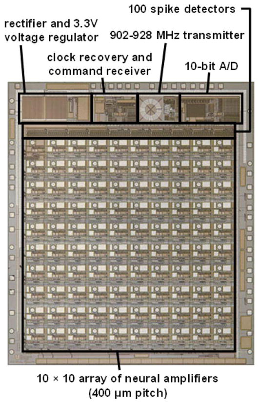
Microphotograph of 5.4 × 4.7 mm2 INI3 wireless neural recording chip, fabricated in a commercially available 0.6-μm 2P3M BiCMOS process.
Fig. 2.
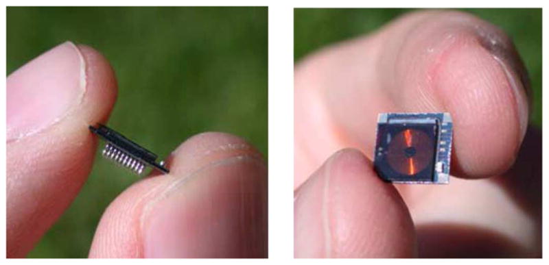
Photograph of prototype INI assembly (side view and top view). The integrated circuit is bonded to the back of a UEA, and a gold 5-mm power/command receive coil is placed over the back of the chip. A surface-mount 100 nF capacitor is visible in the lower right side of the assembly.
Each on-chip amplifier has a gain of 60 dB with globally-programmable high- and low-frequency cutoffs that typically pass signals between 250 Hz and 5 kHz. One of the 100 amplifier channels has a low-frequency cutoff below 0.1 Hz to allow for the recording of local field potentials (LFPs). One user-selected amplifier is digitized at 15.7 kSps by a 10-bit successive-approximation analog-to-digital converter (ADC). A resolution of 10 bits allows for an electrode-referred quantization step of 2.0μV—less than half the rms noise level of the amplifier—with a full-scale range of ±1.0 mV, which is larger than most spikes. Digitizing all 100 channels in parallel would produce prohibitively high data rates given the power constraints of our RF transmitter.
Instead, we limit the telemetry data rate to practical levels by connecting 100 “spike detector” circuits to the amplifier array (see Fig. 3). These spike detectors use comparators to detect neural action potentials (spikes) that exceed a user-programmable threshold either in the positive or negative direction. The 6-bit DACs used to set individual thresholds for each channel are incorporated into the 100 neural amplifier blocks. The programmable threshold levels also accommodate small offsets (on the order of 20μV, input referred) that vary across the amplifier array. The 100 latched comparators used for threshold crossing detection are grouped above the amplifier array to separate noisy digital circuits from sensitive analog amplifiers. The design strategies used to minimize amplifier power dissipation and reduce data rate have previously been described in [10]. The use of simple, single-threshold-based spike detectors greatly reduces the required telemetry data rate but does not permit spike sorting if multiple neurons are observed on the same electrode. By simultaneously transmitting the fully-digitized waveform from one user-selectable amplifier, the spike detection thresholds may be easily set to the desired levels.
Fig. 3.

Functional block diagram of INI3 microchip.
As shown in Fig. 3, additional on-chip circuits rectify the ac voltage on the power receiving coil and produce a regulated 3.3 V dc supply for the chip. (The chip can function properly with a supply voltage from 3 to 4 V.) A 2.765-MHz inductive link supplies power to the chip; additional circuits recover this frequency and divide it by eight to produce a 345.6 kHz on-chip system clock with 50% duty cycle. Commands are sent to the chip by modulating the amplitude of the power signal. An on-chip command receiver detects amplitude changes in the unregulated voltage, waits for a specific 8-bit header signal, then reads in 852 control bits at a rate of 16 kbps. The control bits are used to set spike detection threshold levels and polarities, select a channel for the ADC, power down amplifiers that are not being used, set amplifier bandwidths, and configure the RF transmitter (see [3] for more circuit details).
To relay ADC and spike detector telemetry data to an external station, we implement a frequency-shift keying (FSK) RF transmitter operating in the FCC-approved 902–928 MHz ISM (Industrial, Scientific, Medical) band. Prior versions of the INI chip employed a power-optimized CMOS LC voltage-controlled oscillator (VCO) as a wireless transmitter [3]. This configuration required a high-resolution DAC to set the carrier frequency through the analog VCO control voltage. This approach was highly susceptible to frequency drift due to supply noise and temperature and power supply variations because the VCO was operated on a high-gain portion of its tuning curve.
To combat the problem of temperature and supply dependence, the transmitter core has been redesigned as a digitally-controlled oscillator (DCO), shown in Fig. 4. The architecture of a DCO is identical to a VCO, but rather than relying on the output voltage of a DAC to control the varactor capacitance, the capacitance in a DCO is directly controlled by an 8-bit digital control word (see also [11]–[14]). The measured tuning characteristic, shown in Fig. 5, is nearly linear and exhibits a temperature dependence of −96 ppm/°C from 35 C° –39 °C (four times better than previous INI VCOs).
Fig. 4.
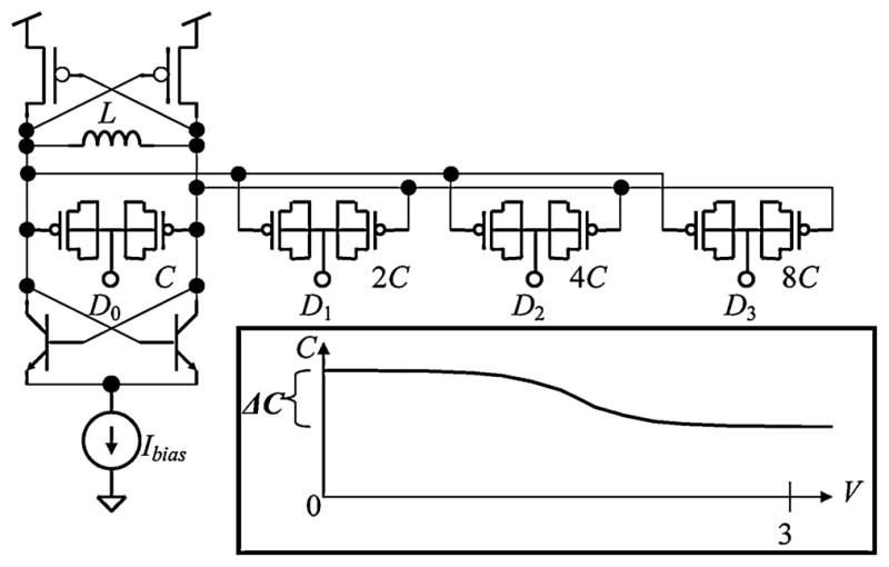
DCO schematic without FSK varactors (only four bits shown for simplicity) and accumulation-mode MOS varactor C-V characteristic (inset).
Fig. 5.
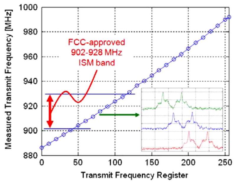
DCO tuning characteristic with measured output spectra for adjacent tuning codes 78, 79, and 80 (green, blue, red) from a range of 0–255.
Direct digital control of the capacitance is accomplished by taking advantage of the sigmoidal C-V curve of an accumulation-mode MOS varactor (see Fig. 4 inset). The small, unit-sized varactors are divided into eight binary-weighted groups (only four bits are shown in Fig. 4 for simplicity), and the control terminal of each group is connected to one of the bits of the control word. When the ith control bit is switched from 0 to 3 V, the total tank capacitance is decreased by 2i Δ C, corresponding to an increase in frequency. Though the relationship between frequency and capacitance is nonlinear, over the frequency range of interest the nonlinearity is mild and acceptable as illustrated in Fig. 5. This technique has no impact on the power dissipation of the oscillator. Furthermore, it is more compact than an approach employing switches and fixed capacitors, and it does not degrade the tank Q. This DCO design reduces temperature and supply dependence as compared to a traditional VCO because all of the varactors are operated at the extremes of the C-V characteristic where the capacitance is far less sensitive to small changes in the control voltage (see Fig. 4 inset).
This digital tuning technique is also used to implement FSK modulation (see Fig. 5 inset). The varactors used for modulation (not shown in Fig. 4) are approximately half the size of the unit varactor in the tuning array. With two additional control bits, the FSK frequency spacing is programmable from 165 to 660 kHz. The overall power dissipation of the RF transmitter is 500μW, a 10× improvement over previous INI VCO designs. This large improvement is due to the shift in process technology from 0.5-μm CMOS to a 0.6-μm BiCMOS process with a thick top metal layer. The minimum power dissipation of LC oscillators required to sustain oscillation is a function of inductor losses [15]. Using this low-resistance metal, it was possible to design a 26-nH inductor with quality factor of Q = 11 at 900 MHz, dramatically decreasing the power dissipation of the circuit. Additionally, the use of bipolar npn transistors in the −gm cell improves power dissipation by maximizing the design’s gm/Ibias ratio and reducing device-related parasitic capacitances.
To complete the wireless interface to the INI3 chip, custom printed circuit boards were designed to send power and commands and receive telemetry data (see Fig. 6). The power board uses a class E power amplifier to create a ~60 V pk 2.765-MHz waveform from a 5 V supply and drive a 5.8-cm-diameter, 28-turn printed-circuit coil. The resulting ac magnetic field powers the INI3 chip. Techniques described in [16] were used to optimize the power link. A USB link to a laptop PC allows the user to send command strings that modulate the amplitude of the coil voltage; the INI3 chip can be completely reprogrammed in less than 100 ms.
Fig. 6.
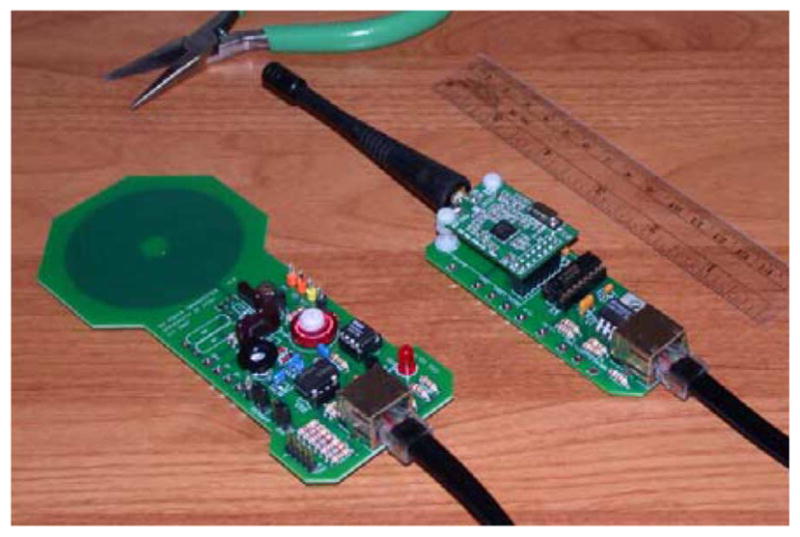
Custom circuit boards supporting wireless power and data link to INI3 chip. Left: 2.765-MHz inductive power/command unit with 5.8-cm printed-circuit coil. Right: 902–928 MHz RF telemetry receiver unit.
The telemetry receiver board implements a 900-MHz FSK demodulator with programmable center frequency and USB interface. Demodulated data are streamed to the PC at the INI3 transmission rate of 345.6 kb/s. PC software locates frame markers generated by the chip, checks parity bits, and decodes the data. A software interface displays the waveform digitized by the ADC at two time scales: a 100 ms window showing a continuously streaming waveform and a 2 ms window showing the most recent time-aligned spikes (see Fig. 7). A third window plots a running graph of bit error rate (BER), which is calculated by checking the parity bits generated by the INI3 chip. If an ADC sample contains a parity error, its value may be interpolated from the previous and following samples to reduce glitches in the waveform. The bottom window displays spike rasters from all 100 spike detectors on the chip.
Fig. 7.
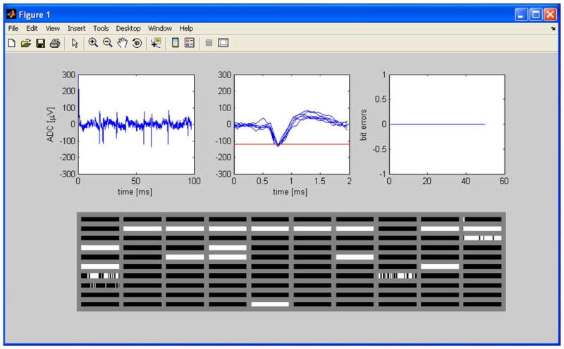
Screenshot of telemetry receive software. Upper left windows show amplifier/ADC waveform at different time scales. Upper right window shows running plot of telemetry bit errors, and the bottom plot shows 100 spike rasters from on-chip spike detectors. Only one amplifier was connected during this experiment, so spike detector data is invalid.
To facilitate chip testing before complete integration to a UEA, we packaged several bare chip die in plastic quad flat pack (QFP) packages and soldered some of these to small circuit boards (see Fig. 8). Due to space limitations around the periphery of the chip, only 20 of the 100 on-chip amplifiers are available in the packaged chips. Fig. 8 shows the general configuration used for benchtop and in vivo experiments described in the remainder of this paper.
Fig. 8.
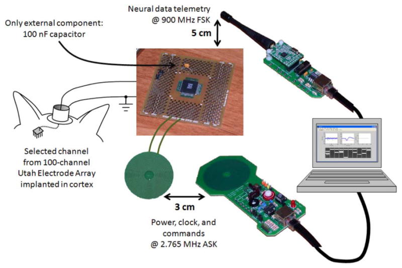
Wireless testing configuration for in vivo experiments using INI3 chip with one external capacitor. Power and commands are delivered wirelessly via inductive link; telemetry is received via 900 MHz antenna.
III. Experimental Results
A. Initial Benchtop Tests
We first tested the INI3 chip by providing a 700 μV, 20 Hz sine wave to the amplifier capable of low-frequency LFP recording. The chip was powered and configured wirelessly as shown in Fig. 8, and telemetry data were obtained via the wireless receiver. Fig. 9 shows a waveform reconstructed from the ADC data from the chip, as well as the spike detector data from that channel. This experiment validated the basic operation of the amplifier, ADC, spike detector, and RF transmitter.
Fig. 9.
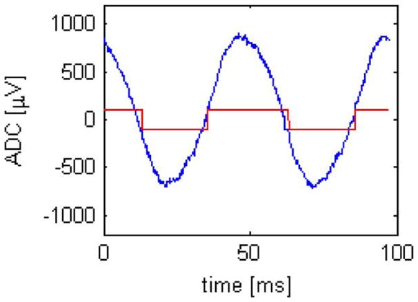
Wirelessly received amplifier/ADC waveform (blue) and spike detector output (red) for a 700 μV, 20 Hz sine wave on wideband channel.
B. Battery-Powered in vivo Operation
Due to a design error in an on-chip bias generator, the neural amplifiers on INI3 exhibited very poor power-supply rejection. When an isolated amplifier was powered from a clean benchtop supply, its input-referred noise was 4.8 μV rms, near the design specification of 5 μV rms. However, when the complete INI3 chip was powered from batteries using the on-chip voltage regulator, the input-referred noise increased to 20–30 μV rms. With wireless inductive power, the input-referred noise increased to 30–40 μV rms. For this reason, some initial experiments were performed using battery power to bypass the on-chip regulator and reduce amplifier noise.
For these experiments, we recorded signals from a 100-channel Utah-style microelectrode array (Cyberkinetics, Inc.) implanted in motor cortex of a cat. Recordings were performed approximately six months after implantation. One amplifier from a packaged INI3 chip was connected to an electrode via a head-mounted connector (see Fig. 8). The cat was awake and resting comfortably during all recordings. The chip was powered from a 3 V battery to reduce power supply noise, but clock and command signals were sent wirelessly over an inductive link. A 5.8-cm receiving coil was connected to the INI3 chip and positioned 3 cm below the transmit coil. The 902–928 MHz telemetry receiver was positioned approximately 5 cm from the INI3 chip to receive data.
Fig. 10 shows time-aligned spikes recorded from six different electrodes during six recording sessions on the same day. (As discussed in Section II, the chip can only transmit the fully-digitized waveform from one amplifier at a time.) Spikes from at least two distinct neurons can be observed in the top two traces.
Fig. 10.
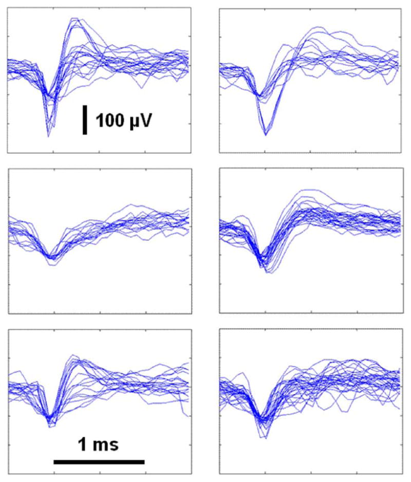
Peak-aligned neural spikes recorded in cat motor cortex from six different electrodes on the same day. The scale in all six graphs is identical. Data were recovered wirelessly using INI3 chip powered with a 3 V battery to reduce power supply noise; clock and command signals were sent wirelessly via an inductive link.
C. Complete Wireless In Vivo Operation
We also obtained neural data using a completely wireless system with no battery. In this experiment, the chip received power, clock, and command signals from the inductive power link. As before, neural data telemetry was transmitted wirelessly approximately 5 cm to a receive antenna. The only off-chip components connected to the INI3 chip were a power receive coil and a 100 nF capacitor (see Fig. 8).
For this experiment, we monitored neural signals from a 100-channel Utah-style microelectrode array (Cyberkinetics, Inc.) implanted in the premotor cortex of a rhesus macaque (Monkey D). Recordings were performed more than 22 months after implantation. As before, one channel of the INI3 chip was wired to an existing head-mounted connector. The chip was positioned near the head during recordings, and the boards in Fig. 6 were used for all power and communication.
Fig. 11 shows several time-aligned spikes recorded with this completely wireless system. Due to the low signal-to-noise ratio, we conducted a simple experiment to confirm that the signals we observed were in fact neural spikes. We recorded neural data in 5-s trials and counted the number of spikes that exceeded a fixed threshold in this time. In some trials, the monkey was resting. In others, the monkey was actively reaching for a target. Fig. 12 shows the number of spikes in ten such trials, extracted in software after receiving the digitized waveform from one selected amplifier channel. Clearly, the neural signal is being modulated by reaching activity.
Fig. 11.

Spikes recorded from monkey premotor cortex during completely wireless operation: no battery was used; power, clock, and command signals were sent using a coil, and telemetry was received using an antenna.
Fig. 12.
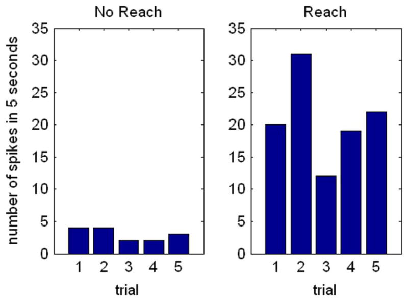
Spike counts recorded from monkey premotor cortex during completely wireless operation as in Fig. 11.
IV. Conclusion
We have demonstrated wireless, inductively-powered neural recording from a cat and a nonhuman primate using a single-chip system with a minimal number of off-chip components. The INI3 chip is sufficiently small and low-power to permit implantation in future systems. The total power consumed by the INI3 chip is 8 mW. Of this, the 100 neural signal amplifiers consume 44% of the total power, the 100 spike detectors consume 22%, the voltage regulator consumes 13%, the RF transmitter consumes 9%, the ADC consumes 6%, and the command and clock recovery circuitry consumes 6%. The dramatic improvement in the RF transmitter power dissipation opens up the possibility of including a complete PLL frequency synthesizer in future INI chips to lock the transmission frequency to a multiple of the clock frequency.
Since the INI3 transmitter does not use an off-chip antenna, its transmission range is limited to a few centimeters. While this is sufficient for transcutaneous links in medical devices, there are many scientific applications where additional range would be useful. To this end, we included an on-chip differential class A output stage capable of driving an external antenna. Additional power may be allocated to this output stage, resulting in a transmission range of several meters, as described in the companion paper [6].
A new version of the INI3 chip has been designed to correct the poor power supply rejection observed here. Initial tests of an improved system show noise levels of 5 μV rms under wireless power. This chip will be integrated with a Utah Electrode Array to create a fully implantable Integrated Neural Interface (see Fig. 2) that should have applications in both neuroscience and medicine.
Acknowledgments
We authors would like to thank Dr. P. House and M. Risch for expert surgical assistance, and D. Haven for technical consultation.
The work of R. R. Harrison was supported in part by the NSF CAREER award ECS-0134336 and in part by the NIH/NINDS Contract N01-NS-4-2362. The work of F. Solzbacher was supported by the NIH/NINDS under Contract N01-NS-4-2362. The work of K. V. Shenoy was supported by the NIH/NINDS under Contract N01-NS-4-2362, in part by the Burroughs Wellcome Fund Career Award in the Biomedical Sciences, in part by The Christopher Reeve Paralysis Foundation, in part by the McKnight Endowment Fund for Neuroscience, in part by the Stanford Center for Integrated Systems, in part by the NSF Center for Neuromorphic Systems Engineering at Caltech, in part by the ONR, and in part by the Sloan Foundation. The work of C. A. Chestek was supported in part by the Johns Hopkins Applied Physics Laboratory under the DARPA Revolutionizing Prosthetics program under Contract N66001-06-C-8005, in part by the NSF Graduate Research Fellowships, and in part by the William R. Hewlett Stanford Graduate Fellowship. The work of V. Gilja was supported in part by the NSF Graduate Research Fellowship and in part by NDSEG Fellowship. The work of P. Nuyujukian was supported by the Stanford Medical Scholars Program. The work of S. Ryu was supported by The Christopher Reeve Paralysis Foundation.
Biographies
Reid R. Harrison (S’98–M’00) was born in De-Funiak Springs, FL. He received the B.S. degree in electrical engineering from the University of Florida, Gainesville, in 1994 and the Ph.D. degree from the California Institute of Technology, Pasadena, in 2000.
He joined the University of Utah, Salt Lake City, in 2000, where he is now an Associate Professor of Electrical and Computer Engineering and an Adjunct Associate Professor of Bioengineering. His research interests include low-power analog and mixed-signal CMOS circuit design, integrated electronics for neural interfaces and other biomedical devices, and biologically inspired computation.
Dr. Harrison received the National Science Foundation CAREER Award in 2002, and in 2006 he received the Jack Raper Award for Outstanding Technology Directions Paper from the International Solid-State Circuits Conference (ISSCC). He has served on the technical program committees of ISSCC and the IEEE International Symposium on Circuits and Systems (ISCAS).

Ryan J. Kier (S’03) received the B.S. and M.S. degrees in electrical engineering from the University of Utah, Salt Lake City, in 2004. His thesis work involved the implementation of neurally-inspired circuits in analog VLSI. He is currently working toward the Ph.D. degree at the University of Utah, where his research interests include low-power VCO design and integrated inductor optimization.
Cynthia A. Chestek (S’04) received the B.S. and M.S. degrees in electrical engineering from Case Western Reserve University, Cleveland, OH, in 2003 and 2005. She is currently working toward the Ph.D. degree in electrical engineering at Stanford University, Stanford, CA.
Her research is focused on neural prosthetic systems.
Ms. Chestek was awarded the National Science Foundation Fellowship and the William R. Hewlett Stanford Graduate Fellowship.

Vikash Gilja received S.B. degrees in electrical engineering and computer science and brain and cognitive sciences in 2003 and the M.Eng. degree in electrical engineering and computer science in 2004 from the Massachusetts Institute of Technology, Cambridge. He is currently working toward the Ph.D. degree in computer science at Stanford University, Stanford, CA.
At Stanford, he joined the Neural Prosthetics Laboratory. His research interests center around the design of practical and robust neural prosthetics systems.
Mr. Gilja is the recipient of awards and honors including the National Defense Science and Engineering Graduate Fellowship and the National Science Foundation Graduate Fellowship.

Paul Nuyujukian (S’03) received the B.S. degree in cybernetics from the University of California, Los Angeles, in 2006. He is currently a third year M.D./Ph.D. candidate studying bioengineering at Stanford University, Stanford, CA.

Stephen I. Ryu received the B.S. and M.S. degree in electrical engineering from Stanford University, Stanford, CA, in 1994 and 1995, respectively, and the M.D. degree from the University of California at San Diego, La Jolla, in 1999. He completed neurosurgical residency and fellowship training at Stanford University in 2006.
He was on faculty as an Assistant Professor of Neurosurgery at Stanford University until 2009. He now practices at the Palo Alto Medical Foundation in Palo Alto, CA. His research interests include brain–machine interfaces, neural prosthetics, minimally invasive neurosurgery, and stereotactic radiosurgery.
Bradley Greger (M’06) was born in Los Angeles, CA. He received the B.A. degree in philosophy and the B.S. degree in biology from Washington State University, Pullman, in 1994 and 1995, respectively. He received the Ph.D. degree in neuroscience from Washington University, St. Louis, in 2001. He was a Postdoctoral Fellow at the California Institute of Technology, Pasadena, until 2006.
He joined the University of Utah, Salt Lake City, in 2006 and is an Assistant Professor of Bioengineering and an Adjunct Assistant Professor of Ophthalmology. He has 14 refereed publications, 20 review papers and abstracts, and two patents since 1995 in the fields of neuroscience and bioengineering.

Florian Solzbacher (M’04) received the M.Sc.EE from the Technical University Berlin in 1997 and the Ph.D. degree from the Technical University Ilmenau in 2003.
He is Director of the Microsystems Laboratory at the University of Utah, Co-Director of the Utah Nanotechnology Institute, President of Blackrock Microsystems and holds faculty appointments in Electrical and Computer Engineering, Materials Science and Bioengineering. His research focuses on harsh environment microsystems and materials, including implantable, wireless microsystems for biomedical and healthcare applications, but also high temperature and harsh environment compatible micro sensors. He is co-founder of several companies such as Blackrock Microsystems, First Sensor Technology and NFocus. He is Chairman of the German Association for Sensor Technology AMA, and serves on a number of company and public private partnership advisory boards. He is author of over 100 journal and conference publications, five book chapters, and 16 pending patents.
Krishna V. Shenoy (S’87–M’01–SM’06) received the B.S. degree in electrical engineering from the University of California, Irvine, in 1990, and the S.M. and Ph.D. degrees in electrical engineering from the Massachusetts Institute of Technology, Cambridge, in 1992 and 1995.
He was a neurobiology postdoctoral fellow at Caltech from 1995 to 2001 and then joined the Stanford University faculty where he is an Associate Professor in the Departments of Electrical Engineering and Bioengineering, and in the Neurosciences Program. His research interests include computational motor neurophysiology and neural prosthetic system design.
Dr. Shenoy received the 1996 Hertz Foundation Doctoral Thesis Prize, a Burroughs Wellcome Fund Career Award in the Biomedical Sciences, an Alfred P. Sloan Research Fellowship, and a McKnight Endowment Fund in Neuroscience Technological Innovations in Neurosciences Award.
Contributor Information
Reid R. Harrison, Email: harrison@ece.utah.edu, Department of Electrical and Computer Engineering and the Department of Bioengineering, University of Utah, Salt Lake City, UT 84112 USA.
Ryan J. Kier, Department of Electrical and Computer Engineering, University of Utah, Salt Lake City, UT 84112 USA.
Cynthia A. Chestek, Department of Electrical Engineering, Stanford University, Stanford, CA 94305 USA.
Vikash Gilja, Department of Computer Science, Stanford University, Stanford, CA 94305 USA.
Paul Nuyujukian, School of Medicine, Stanford University, Stanford, CA 94305 USA.
Stephen Ryu, Department of Neurosurgery, Stanford University, Stanford, CA 94305 USA.
Bradley Greger, Department of Bioengineering, University of Utah, Salt Lake City, UT 84112 USA.
Florian Solzbacher, Department of Electrical and Computer Engineering and the Department of Bioengineering, University of Utah, Salt Lake City, UT 84112 USA.
Krishna V. Shenoy, Department of Electrical Engineering and the Neurosciences Program, Stanford University, Stanford, CA 94305 USA.
References
- 1.Hochberg LR, Serruya MD, Friehs GM, Mukand JA, Saleh M, Caplan AH, Branner A, Chen D, Penn RD, Donoghue JP. Neuronal ensemble control of prosthetic devices by a human with tetraplegia. Nature. 2006;442:164–171. doi: 10.1038/nature04970. [DOI] [PubMed] [Google Scholar]
- 2.Mohseni P, Najafi K, Eliades SJ, Wang X. Wireless multichannel biopotential recording using an integrated FM telemetry circuit. IEEE Trans Neural Syst Rehabil Eng. 2005 Sep;13(3):263–271. doi: 10.1109/TNSRE.2005.853625. [DOI] [PubMed] [Google Scholar]
- 3.Harrison RR, Watkins PT, Kier RJ, Lovejoy RO, Black DJ, Greger B, Solzbacher F. A low-power integrated circuit for a wireless 100-electrode neural recording system. IEEE J Solid-State Circuits. 2007 Jan;42(1):123–133. [Google Scholar]
- 4.Töpper M, Klein M, Wilke M, Oppermann H, Kim S, Tathireddy P, Solzbacher F, Reichl H. Packaging concepts for neuroprosthetic implants. Proc. Eur. Microelectron. Packag. Conf. (EMPC 2007); Oulu, Finland. Jun. 17–20, 2007. [Google Scholar]
- 5.Kim S, Tathireddy P, Normann RA, Solzbacher F. Thermal impact of an active 3-D microelectrode array implanted in the brain. IEEE Trans Neural Syst Rehabil Eng. 2007 Dec;15(4):493–501. doi: 10.1109/TNSRE.2007.908429. [DOI] [PubMed] [Google Scholar]
- 6.Chestek CA, Gilja V, Nuyujukian P, Kier RJ, Solzbacher F, Ryu SI, Harrison RR, Shenoy KV. HermesC: RF wireless low-power neural recording system for freely behaving primates. IEEE Trans Neural Syst Rehabil Eng. 2009 Aug;17(4):321–347. doi: 10.1109/TNSRE.2009.2023293. [DOI] [PubMed] [Google Scholar]
- 7.Harrison RR, Kier RJ, Chestek CA, Gilja V, Nuyujukian P, Ryu SI, Greger B, Solzbacher F, Shenoy KV. Wireless neural signal acquisition with single low-power integrated circuit. Proc. 2008 IEEE Int. Symp. Circuits Syst. (ISCAS 2008); Seattle, WA. 2008; pp. 1748–1751. [Google Scholar]
- 8.Chestek CA, Gilja V, Nuyujukian P, Kier RJ, Solzbacher F, Ryu SI, Harrison RR, Shenoy KV. HermesC: RF wireless low-power neural recording for freely behaving primates. Proc. 2008 IEEE Int. Symp. Circuits Syst. (ISCAS 2008); Seattle, WA. 2008; pp. 1752–1755. [Google Scholar]
- 9.Kim S, Zoschke K, Klein M, Black D, Buschick K, Toepper M, Tathireddy P, Harrison R, Oppermann H, Solzbacher F. Switchable polymer-based thin film coils as a power module for wireless neural interfaces. Sensors Actuators A. 2007;136:467–474. doi: 10.1016/j.sna.2006.10.048. [DOI] [PMC free article] [PubMed] [Google Scholar]
- 10.Harrison RR. The design of integrated circuits to observe brain activity. Proc IEEE. 2008 Jul;96(7):1203–1216. [Google Scholar]
- 11.Da Dalt N, Thaller E, Gregorius P, Gazsi L. A compact triple-band low-jitter digital LC PLL with programmable coil in 130-nm CMOS. IEEE J Solid-State Circuits. 2005 Jul;40:1482–1490. [Google Scholar]
- 12.Staszewski RB, Hung C, Barton N, Lee M, Leipold D. A digitally controlled oscillator in a 90 nm digital CMOS process for mobile phones. IEEE J Solid-State Circuits. 2005 Nov;40:2203–2211. [Google Scholar]
- 13.Roham M, Halpern JM, Martin HB, Chiel HJ, Mohseni P. Wireless amperometric neurochemical monitoring using an integrated telemetry circuit. IEEE Trans Biomed Eng. 2008 Nov;55(11):2628–2634. doi: 10.1109/TBME.2008.2001264. [DOI] [PMC free article] [PubMed] [Google Scholar]
- 14.Yin M, Ghovanloo M. Wideband flexible transmitter and receiver pair for implantable wireless neural recording applications. Proc. IEEE Northeast Workshop Circuits Syst. (NEWCAS); 2007. pp. 85–88. [Google Scholar]
- 15.Kier RJ, Harrison RR. Power minimization of a 433-MHz LC VCO for an implantable neural recording system. Proc. 2006 IEEE Int. Symp. Circuits Syst.(ISCAS 2006); Kos, Greece. 2006. pp. 3225–3228. [Google Scholar]
- 16.Harrison RR. Designing efficient inductive power links for implantable devices. Proc. 2007 IEEE Int. Symp. Circuits Syst. (ISCAS 2007); New Orleans, LA. 2007. pp. 2080–2083. [Google Scholar]