Abstract
We demonstrate porous silica surface modification, combined with microcontact printing, as an effective method for enhanced protein patterning and adsorption on arbitrary surfaces. Compared to conventional chemical treatments, this approach offers scalability and long-term device stability without requiring complex chemical activation. Two chemical surface treatments using functionalization with 3-aminopropyltriethoxysilane (APTES) and glutaraldehyde (GA) were compared with the nanoporous silica surface on the basis of protein adsorption. The deposited thickness and uniformity of the porous silica films were evaluated for fluorescein isothiocyanate (FITC)-labeled rabbit immunoglobulin G (R-IgG) protein printed onto the substrates via patterned polydimethlysiloxane (PDMS) stamps. A more complete transfer of proteins was observed on porous silica substrates compared to chemically functionalized substrates. A comparison of different pore sizes (2–6 nm), and porous silica thicknesses (30–200 nm) indicates that porous silica with 4 nm diameter, 57% porosity and a thickness of 96 nm provided a suitable environment for complete transfer of R-IgG proteins. Both fluorescence microscopy and atomic force microscopy (AFM) were used for protein layers characterizations. A porous silica layer is biocompatible, providing a favorable transfer medium with minimal damage to the proteins. A patterned immunoassay microchip was developed to demonstrate the retained protein function after printing on nanoporous surfaces, which enables printable and robust immunoassay detection for point-of-care applications.
Keywords: Porous sílica, microcontact printing, Polydimethylsiloxane (PDMS), Proteins, IgG
I. Introduction
Microcontact printing (µCP) is a stamping based method for the dry transfer of molecules onto a surface[1–3]. The method, introduced by Whitesides in 1993[4, 5] and extended to the transfer of protein molecules by Bernard et al. in 2000[6], has received much scientific attention as a means to immobilize proteins in controlled patterns for biomedical applications such as biosensors and immunoassays[7–13]. Patterning of biomolecules onto a solid substrates is relevant to providing controlled biocompatible surfaces[14, 15]. Microcontact printing may be used to pattern multiple proteins on the same substrate, thus allowing for biological assays with greater diagnostic power[16–19]. A number of possible applications would be enabled if the same surface could be patterned with proteins of different types[20, 21]. In this paper, we compared the efficiency of protein transfer via µCP onto porous silica coated, 3-aminopropyltriethoxysilane (APTES) treated, glutaraldehyde (GA) treated, and untreated glass substrates.
Substrate surfaces are often functionalized to increase their affinity for specific proteins [13, 22]. Common functionalization procedures for preparing surfaces for protein binding utilize silane compounds with terminal functional groups that interact electrostatically or covalently with protein surface groups to increase protein adsorption. Two common chemicals used for surface functionalization are APTES, chemical formula (NH2-(CH2)3-Si(OC2H5)3, and GA, chemical formula (CHO-(CH2)3-CHO)[23–28]. The silane end of the APTES molecule binds covalently to surface silicon atoms, and the amino end of the molecule increases protein adsorption to the surface through electrostatic interactions. The linear glutaraldehyde molecule is terminated on both ends by aldehyde groups and thus may be used to transform surface amino groups to surface aldehyde groups. These aldehyde groups covalently bind proteins through the Schiff base reaction[22]. While the use of chemical treatments is often effective at increasing adsorption of protein, it requires complex chemical activation and introduces problems such as stresses around the silane-substrate interface that can occur during temperature cycling, or atmospheric water hydrolyzing either the oxane bonds between silane and substrate or the bonds between the organo-functional group of the silane and the organic molecule[8].
Previously, porous silica thin films have been used for the size-selective trapping proteins from a biological complex, such as human serum[29],[30, 31]. We have designed and characterized a large set of porous silica thin films with various pore nanotextures to enhance the capacity and efficiency of specific protein enrichment[29]. Here we show that a thin layer of porous silica can be used to improve the efficiency of protein transfer to a surface via µCP. Porous silica can be deposited in an inexpensive procedure based on spin coating that requires no specialized techniques such as sputtering or chemical vapor deposition. The porous silica here is created on solid substrates by using tri-block copolymers as structural direction agents mixed with silica solution and deposited over the surface. Once the porous silica was created subsequent deposition of proteins was performed using microcontact printing. The study reported herein has potential applications such as patterned integrated micro-devices, for immunoassay detection, micro-total analysis systems and other biomedical point of care applications. Porous silica has long term stability and is compatible with mainstream microfabrication processes in the semiconductor industry.
II. Preparation of Porous Silica
1. Fabrication of mesoporous silica thin films
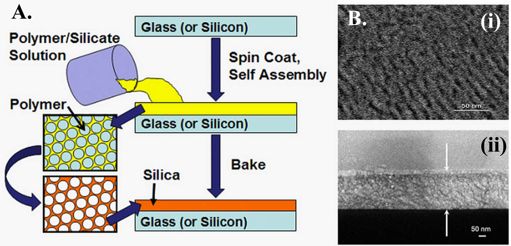
A typical preparation of the porous silica thin film was carried out as follows (Figure 1).
Figure 1.
(a). Schematic of porous silica preparation. (b) Scanning electron micrograph (SEM) of porous silica (i) Top view (ii) Side View. Arrows indicate the thickness of the porous silica on Silicon, 223 nm.
Tetraethyl orthosilicate (TEOS) (14ml) was dissolved in a mixture of 15 ml of ethanol, 6.5 ml of distilled water, and 0.3 ml of 6M HCl and stirred for 2 hours at 75°C to form a clear silicate sol. Separately, 1.8 g of F127, a di-functional block copolymer surfactant, was dissolved in 60 ml of ethanol by stirring at room temperature. Triblock copolymer PEO106-PPO70-PEO106 (Pluronic F127) was selected as the synthetic template in this study. F127 with its high molecular weight, versus other copolymers studied herein, possesses a higher degree of structural periodicity and more uniformed pore size distribution in their nanoporous thin film product, which facilitate the enrichment of targeted protein harvesting.
The coating solution was prepared by mixing 7.5 ml of the silicate sol into the triblock copolymer solution followed by stirring of the resulting sol for 2 hours at room temperature. The pH of the mixture solution remained around 1.5. The coating sol was deposited on a silicon (1 0 0) wafer by spin-coating at a spin rate of 1500 rpm for 20 seconds. To increase the degree of polymerization of the silica framework in the films and to further improve their thermal stability, the as-deposited films were heated at 80 °C for 12 hours. The films were calcinated at 425°C to remove the organic surfactant. The temperature was raised at a heating rate of 1°C per min, and the furnace was heated at 425°C for 5 hours. The films produced were transparent and without cracks. Oxygen plasma ashing was performed in a Plasma Asher (March Plasma System) to pre-treat the chip surface. The treatment was carried out with an O2 flow rate at 80 sccm and a power of 300 W for 10 minutes. The thickness of the thin film could be controlled by adjusting the concentration of polymer in the precursor solution, while the porosity mainly depends on the molar ratio of polymer and silicate in the starting material.
2. Characterization Techniques
We utilized several characterization techniques to study the spin-coated mesoporous silica thin films. Through the use of a variable angle spectroscopic ellipsometer (J. A. Woollam Co. M-2000DI) and WVASE32 modeling software, the thickness of thin films and their porosities were measured in the Cauchy model and the Effective Medium Approximation (EMA) model, respectively. Ellipsometric optical quantities, the phase (Δ), and amplitude (ψ) were carried by requiring spectra for 65°, 70°, and 75° incidence angels using wavelengths from 300 to 1600 nm. In the Cauchy model, the top layer’s thickness and reflective index were determined by fitting experimental data with the model and minimizing the mean square error. Using the EMA model, the films’ porosities were calculated by assuming a certain volume of void in the pure silica and setting the top layer’s thickness obtained by the Cauchy model as the constant. X-ray diffraction (XRD) patterns were obtained on Philips X’Pert-MPD system with Cu Kα ray (45 kV, 40mA). θ–2θ scans were recorded from all spin-coated films at 1s/0.001° steps over the angle range from 0.2° to 6°. Transmission electron microscopy (TEM; FEI Technai; FEI Co.) was used to obtain micrographs of the plane view of the porous silica thin films at a high tension of 200 kV. Scanning electron microscopy (SEM; Ziess SEM Neon 40) was used to acquire top and side vies of the films; Figure 1b shows one variety of film which is 223 nm thick with 53% porosity and 4.0 nm pore diameter.
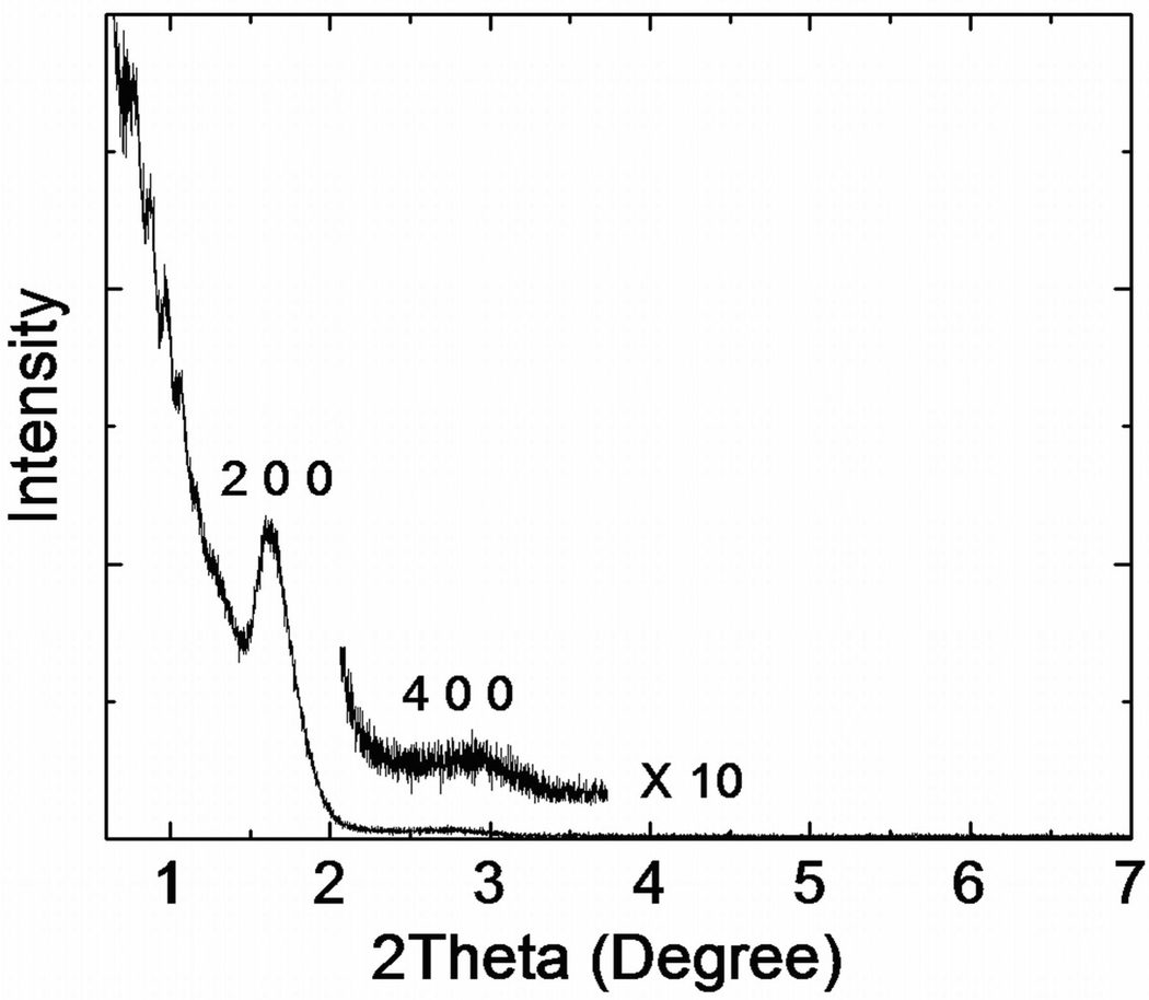
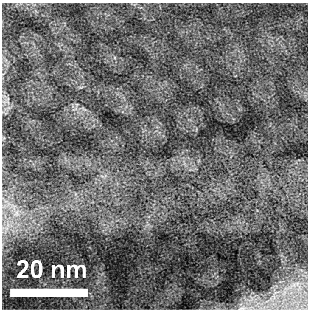
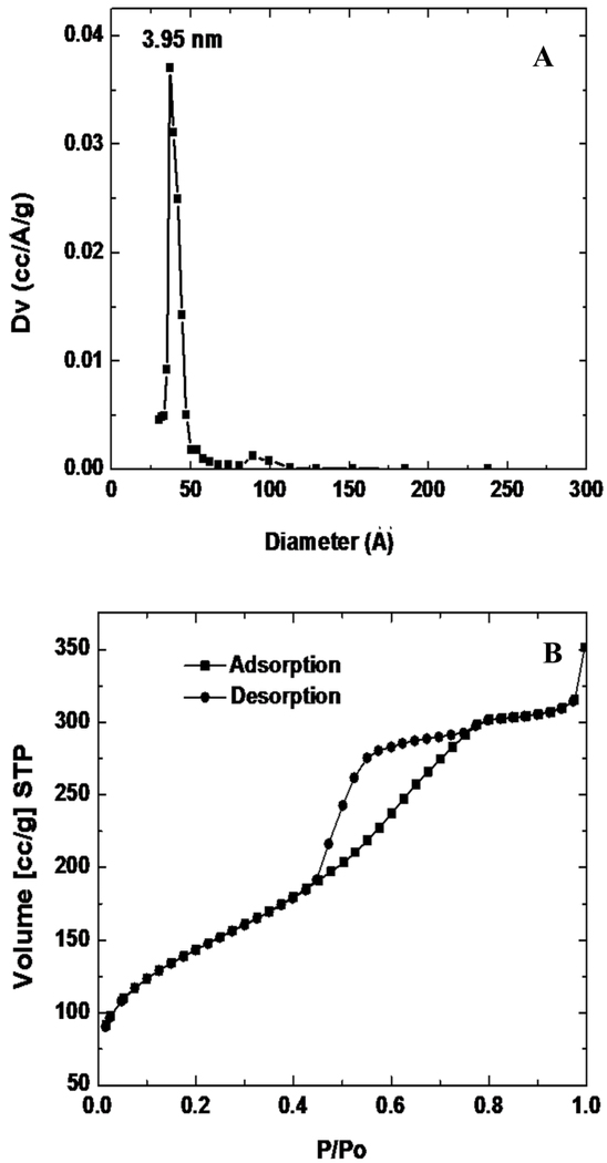
N2 adsorption/desorption analysis was used to measure surface area and pore size distribution. Quantachrome was used to record the N2 adsorption/desorption isotherm at 77 K on the full range of relative P/P0 pressures. Brunauer-Emmett-Teller (BET) surface areas were determined over a relative pressure range of 0.05 to 0.4. Nanopore size distributions were calculated from the desorption branch of the isotherms using the Barrett-Joyner-Halenda (BJH) method. XPS spectra were recorded using a X-ray photoelectron spectrometer (Kratos Axis Ultra), utilizing a monochromated Al-Kα X-ray source (hν = 1486.5 eV), hybrid optics (employing a magnetic and electrostatic lens simultaneously) and a multi-channel plate and delay line detector coupled to a hemispherical analyzer. The take-off angle of the photoelectrons was 90°. All spectra were recorded using an aperture slot of 300 × 700 microns, and high-resolution spectra were collected with a pass energy of 20 eV. The pressure in the analysis chamber was typically 2×10⁻⁹ Torr during data acquisition. Kratos XPS analysis software was used to determine the stoichiometry of samples from corrected peak areas and employing Kratos sensitivity factors for each element of interest. The XRD pattern shown in Figure 2 illustrates a 3D honeycomb like nanostructure hexagonally arranged on the substrate, as confirmed by XRD, with peaks at (200) and (400), and further verified through TEM imaging in Figure 3. N2 adsorption/desorption curves were generated using a Quantachrome Autosorb-3b BET Surface Analyzer (inset of Figure 4) and the pore size distribution was calculated using the Barrett-Joyner-Halenda (BJH) method (Figure 4)[32]. The adsorption/desorption isotherms describe a Type IV isotherm with a H2 hysteresis loop (sloping adsorption branch and nearly vertical desorption branch), indicating a nanoporous silica structure with interconnecting channels. Inflection points appearing at 0.40 < P/P0 < 0.75 in Figure 4 indicated the formation of ink-bottle shape nanopores.
Figure 2.
The XRD pattern of porous silica thin film prepared by F127.
Figure 3.
The TEM image of porous silica thin films prepared using Pluronic F127.
Figure 4.
N2 adsorption/desorption analysis (A. pore size distribution and B. isotherms) of the porous silica thin films prepared using Pluronic F127.
III. Experimental
1. Preparation of Substrates
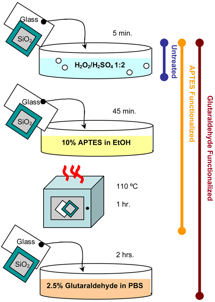
The chemical surface modification procedure can be seen in Figure 5. Control substrates and those to be functionalized with APTES underwent piranha cleaning (H2O2/ 2H2SO4 v/v) for 5 minutes followed by a triple alcohol rinse before being dried in a 110°C oven for 10 minutes. Excluding the control, the samples were then placed in a 10 % (v/v) 3-aminopropyltriethoxysilane/ethanol solution for 45 minutes and subsequently rinsed thoroughly with ethanol and removed to a 110°C oven for 1 hour. Substrates to be functionalized with glutaraldehyde were first cleaned and functionalized with APTES as detailed above. Immediately after being removed from the oven, these substrates were placed in a 2.5% (v/v) glutaraldehyde/phosphate buffered saline (PBS) solution for two hours. The substrates were then rinsed thoroughly with PBS and kept in PBS until just prior to stamping when they were rinsed thoroughly with de-ionized water and dried under a N2 stream.
Figure 5.
Procedure for chemical surface modification of glass and silicon substrates.
The contact angle of functionalized substrates was measured with a goniometer to confirm functionalization. Values shown in Table 1 are consistent with the literature[22, 27, 28, 33, 34]. It was observed that porous silica and untreated glass slides had smaller contact angles than chemically treated substrates.
Table 1.
Contact angles of experimental substrates measured within 12 hours of functionalization with goniometer (First Ten Angrstroms).
| Substrate | Measured Contact Angle (°) |
|---|---|
| Untreated Glass | 13 ± 3° |
| APTES-functionalized Glass (Amine [-NH2] Groups) | 69 ± 7° |
| Glutaraldehyde-functionalized Glass (Aldehyde [-CHO] Groups) | 59 ± 4° |
| Porous Silica* | 13 ± 5° |
Porous silica layer for this measurement has 96 nm thickness, 57% porosity, and 4.0 nm pore diameter.
2. Microcontact Printing Procedure
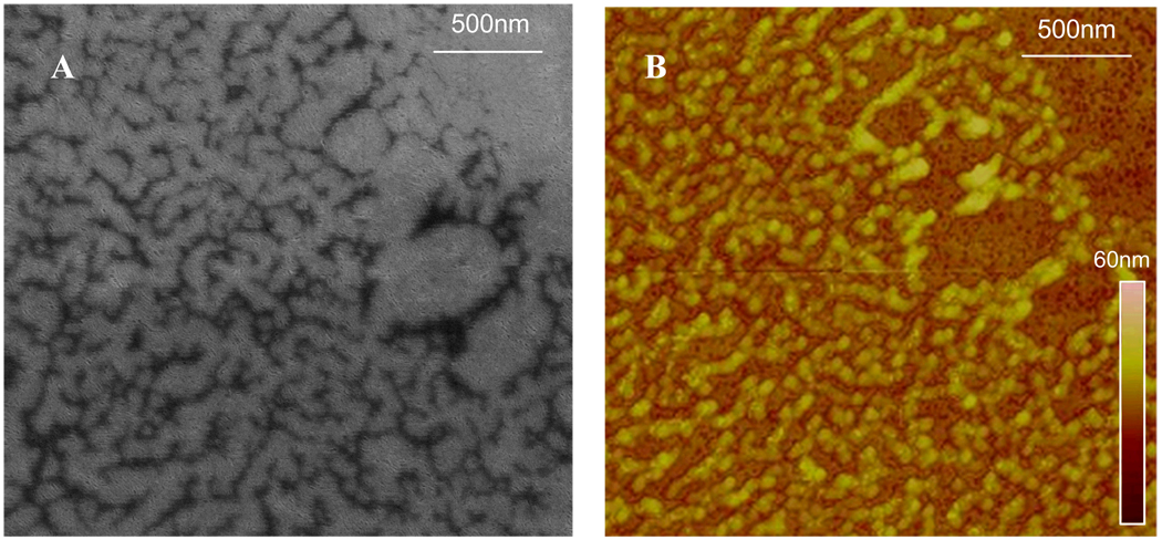
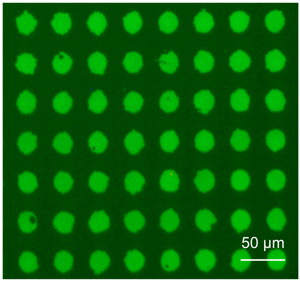
PDMS stamps were fabricated from hard silicon masters[35] to have 20 µm diameter by 20µm high circular features. These stamps were “inked” for 20 minutes with a 5µg/ml solution of FITC-labeled R-IgG (Sigma Aldrich), rinsed sequentially with (0.01 Molar) phosphate buffered saline and deionized water, dried under N2 gas, and finally brought into conformal contact with the target substrate for 60 seconds. A home-built stamping apparatus was used to ensure proper alignment of the polymer stamp and the substrate and to allow for the application of consistent stamping pressures, generally in the range of 40mg/0.5cm2. Transferred protein layers were analyzed by fluorescence (Olympus BX51) and atomic force microscopy (AFM; Digital Instruments Series IV, Veeco). Protein layers deposited on porous silica coated silicon were also analyzed using SEM (Ziess SEM Neon 40), as seen in Figure 6. A fluorescence image of an array of the printed protein can be seen in Figure 7.
Figure 6.
(A) SEM and (B) AFM images of patterned proteins on porous silica on silicon.
Figure 7.
Array of FITC-labeled R-IgG protein microcontact printed (diameter 20 µm) onto porous silica deposited on glass.
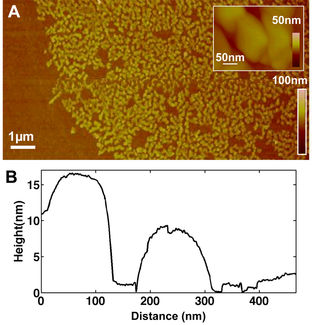
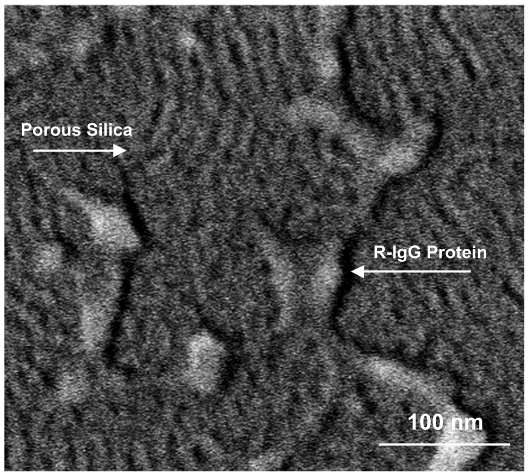
Rabbit IgG protein as imaged by AFM (Figure 8), and SEM (Figure 9) displays the microstructure of the patterned protein. The dimensions of IgG as reported by Lee et al. are 8.5 nm × 14.4 nm × 4 nm[36]. The height dimensions observed for the printed protein molecules are consistent with these accepted dimensions for the R-IgG, supporting the conclusion that the protein has retained its basic shape after stamping[36, 37].
Figure 8.
(A) Atomic Force Microscopy (AFM) of rabbit immunoglobin G (R-IgG) protein on porous silica, indicating a height of (Left peak) 16 nm (Right peak) 8nm. Accepted dimensions of R-IgG are 14.5 nm × 8.5 nm × 4.8 nm (B) Plot of height data for inset image.
Figure 9.
SEM of R-IgG proteins on porous silica on silicon after micro-contact printing.
IV. Results and Discussion
1. Porous Silica Characterization
The coating precursor was prepared starting with self-assembly between polymer units to form the surfactant micelle and mixing it with soluble silicates in homogeneous, hydroalcoholic solutions. The evaporation of solvent during spin coating results in an increase of concentration of polymer in the solution to exceed the critical micelle concentration and drives silica/copolymer self-assembly into a uniform thin-film nanophase. The average pore size and nanostructure throughout the thin film can be precisely tuned by varying such as selection of polymer templates, molar ratio of silicate to polymer, deposition rate and calcination condition.
2. Protein Deposition Uniformity
2.1 Porous Silica Substrate
First, we tested several porous silica conditions to determine the most suitable set of parameters for µCP. Samples shown in Table 2 were used. It was found that porous silica exhibiting 4 nm pores at 57% porosity and with a layer thickness in the range of 30–100 nm provides for the most effective protein transfer in terms of consistency of the full transfer of the stamping pattern, and stamped protein layer thickness and roughness. Protein layers stamped on the porous silica layers with parameters as listed in Table 2 were analyzed with AFM microscopy. As porosity and pore size decrease, the porous silica layer approaches nonporous silica and the advantages of the pores are lost.
Table 2.
Thickness and roughness of multiple porous silica layers measured with AFM (Digital Instruments Series IV). Layer parameters in bolded cells were found to result in the most successful protein transfer.
| Porosity | Thickness | Pore Size |
Contact Angle |
Protein Layer Thickness |
Protein Layer Roughness |
|---|---|---|---|---|---|
| 63% | 547 nm | 6.3 nm | 11.1 ± 0.2° | 3 ± 2 nm | 3 ± 1 nm |
| 39% | 611 nm | 4.0 nm | 13.3 ± 0.7° | 8 ± 5 nm | 3 ± 2 nm |
| 57% | 673 nm | 4.0 nm | 12.8 ± 0.8° | 8 ± 4 nm | 5 ± 2 nm |
| 32% | 561 nm | 2.0 nm | 23 ± 2° | 3 ± 2 nm | 1.5 ± 0.4 nm |
| 57% | 30 nm | 4.0 nm | 30 ± 3° | 5 ± 1 nm | 1.1 ± 0.6 nm |
| 57% | 96 nm | 4.0 nm | 13 ± 6° | 3 ± 1 nm | 3.4 ± 0.4 nm |
| 53% | 223 nm | 4.0 nm | 15 ± 2° | 5 ± 3 nm | 5.0 ± 0.5 nm |
For proteins deposited onto porous silica substrates the resulting height data was divided into regions of protein coverage and regions of background. Eight 1µm2 areas from the area where the regions bordered each other were taken and the height data was averaged over these. The background height was subtracted from the protein layer height to give the data in Table 2. A similar procedure was repeated for roughness measurements. For example, to calculate the protein thickness for the sample shown in Figure 8, the 1µm2 areas had an average height of 4.7 nm, from which the background height of −3.2 nm was subtracted to give a protein layer height of 7.9 nm. From analysis under a bright field microscope, it was concluded that porous silica layers with large pore sizes trap particles of the PDMS stamp, contaminating the transferred protein. Also, as the porous silica layer thickness increases, the surface of the layer develops wide undulations that disrupt conformal contact of the stamp and decrease protein transfer. For these reasons, porous silica layers with pore sizes at or above 6 nm and with layer thicknesses greater than ~200 nm were found to be unfavorable to protein transfer.
Porous silica substrates have an advantage that they can be uniformly processed compared to chemically functionalized substrates. In order to print various proteins onto porous silica substrates, the hole dimensions of the porous layer should be similar or smaller to the smallest dimension of the protein (i.e. In this study we used 4nm holes, and the smallest dimension of the IgG protein was 4nm. Larger pore sizes indicated the diffusion of proteins into the pores with a thickness smaller than that of the protein size as reported in solution based experiments [ref]). The porosity and thickness of the porous silica can be maintained constant by varying the processing conditions.
2.2 Chemically Modified Substrates
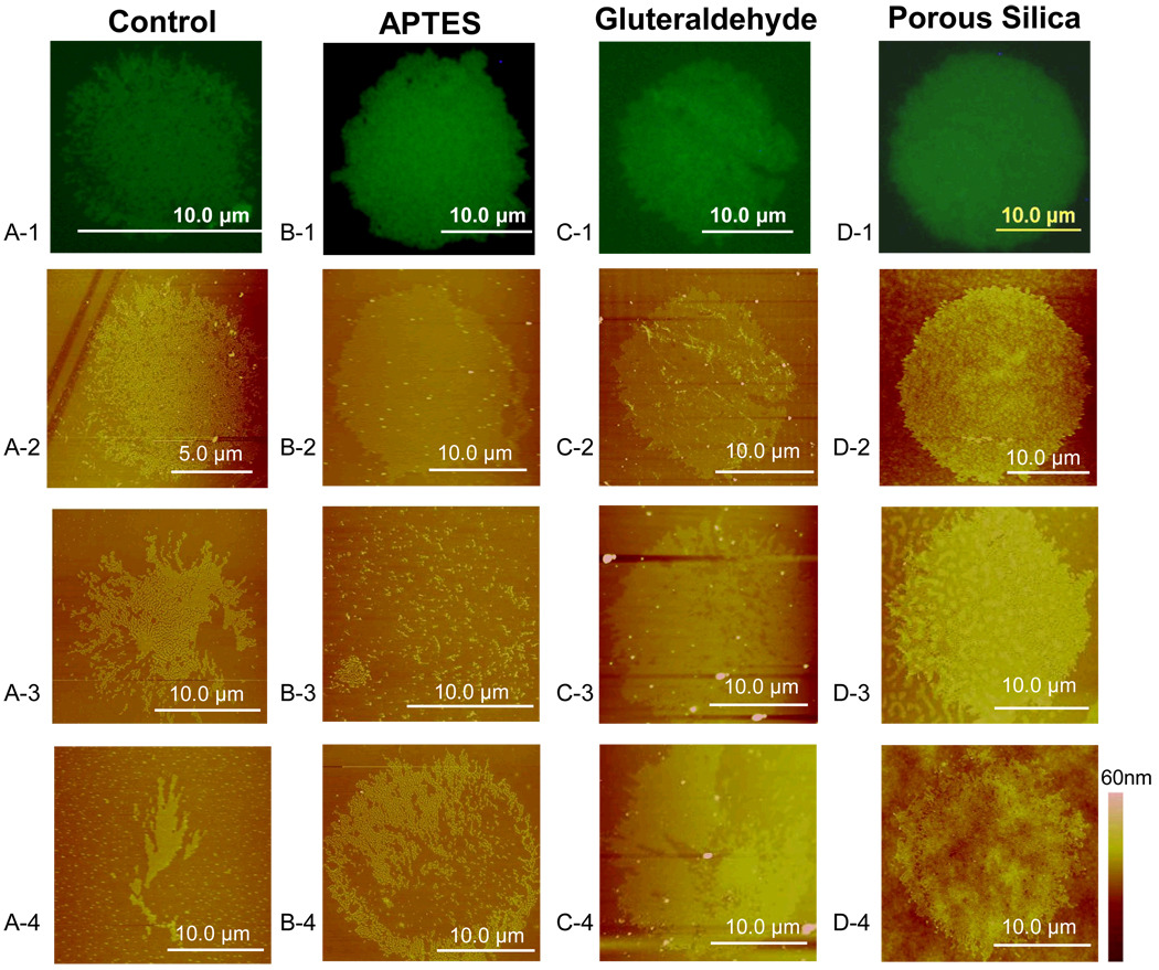
Here we compare µCP on porous silica and chemically-treated surfaces. The porous silica layer used has parameters as found in the previous section; 4 nm pores at 57% porosity and with a layer thickness in the range of 30–100 nm. Results are shown in Figure 10.
Figure 10.
Fluorescence images of 15µm diameter circles of FITC-labeled R-IgG protein deposited with micro-contact printing onto (a) Untreated glass substrate (b) APTES (c) Gluteraldehyde (d) Porous silica treated glass slides. AFM images of corresponding fluorescence images were performed as well as other portions of patterned substrate.
It was observed that completeness of transfer is the highest for porous silica, Figure 10 D-2, and APTES-functionalized surfaces, Figure 10 B-2, partial for the untreated surface, Figure 10 A-3, and low for the glutaraldehyde-functionalized surface, Figure 10 C-3. Relative to the chemically modified and untreated substrates, the porous silica coated substrates provided for thicker and more uniform protein layers. The layers on glutaraldehyde-functionalized surfaces are thin, Figure 10 C-2, as are those on APTES, Figure 10 B-2, averaging 3 and 2 nm thick, respectively, compared to the 5 nm thickness of the layers on porous silica, as seen in Table 3. The average 5 nm protein layer on porous silica is consistent with protein monolayers.
Table 3.
Thickness and roughness of R-IgG protein layers deposited on various substrates. (Measurements taken with Digital Instruments Series IV AFM)
| Substrate | Protein Layer Thickness |
Protein Layer Roughness |
Number of Circles |
Number Points per Circle |
|---|---|---|---|---|
| Porous Silica | 5 ± 2 nm | 0.6 ± 0.3 nm | 4 | 8 |
| Untreated Glass | 4 ± 1 nm | 1.0 ± 0.9 nm | 4 | 8 |
| APTES Treated Glass | 3 ± 2 nm | 1.0 ± 1.0 nm | 4 | 8 |
| Glutaraldehyde Treated | 2 ± 1 nm | 0.5 ± 0.7 nm | 4 | 8 |
Proteins were transferred, onto PoSi and chemically functionalized substrates that were prepared 3 months in advance, using micro-contact printing. The results for PoSi substrate remained consistent with previous results, indicating complete transfer of proteins. The transfer of proteins onto chemically modified substrates was similar to the control slides with non-uniform deposition of proteins onto the substrate.
Protein layers observed on the chemically treated substrates were thinner, 2 to 3 nm thick, than the smallest dimension of the R-IgG protein, 4 nm. This indicates that the R-IgG protein, which is known to bind with surfaces through hydrophobic interactions[38], unfolding to maximize favorable interactions with the APTES (71° contact angle) and Glutaraldehyde (56° contact angle) coated surfaces, as shown in Table 1[37]. The roughness of the protein film deposited on untreated and APTES-modified substrates is 1 nm on average, while the layer on glutaraldehyde-modified substrates averages half of a nanometer, though its maximum value is 1.2 nm. The layer on porous silica is smoother on average at 0.6 nm, with a range of 0.3 to 0.9 nm. Protein layers on untreated glass and APTES-treated glass both exhibited incomplete coverage, while protein circles on glutaraldehyde-treated glass and porous silica were both filled. Arrays of 20 µm diameter circles printed on porous silica were observed to be fully printed while the complete pattern was rarely transferred to the other chemically treated substrates.
Chemical modifications of porous silica substrates have been demonstrated previously for solution based experiment indicating better adsorption of protiens [29]. Chemical modification of porous silica might increase the adsorption of proteins, since the effect of both chemical and physical forces are prominent in attracting the proteins.
3. Integrated Patterned Immunoassay System
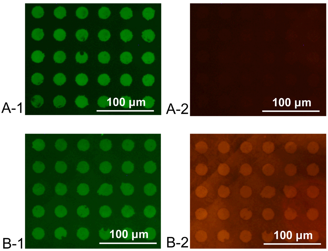
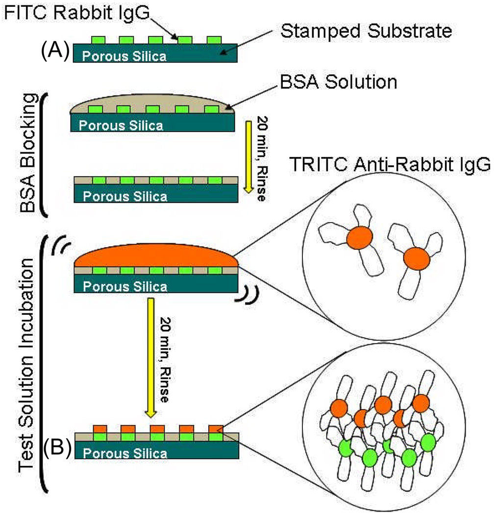
To demonstrate that protein function is retained after immobilization, porous silica was used as the basis for a patterned immunoassay. FITC-labeled R-IgG proteins were stamped onto a porous silica surface with 57% porosity, 4 nm pore size, and 30 nm layer thickness, as described above (Table 2). As exhibited by Figure 12, the surface was then blocked with bovine serum albumin (BSA) and incubated with TRITC-labeled anti-R-IgG protein suspended in phosphate buffered saline for 20mins. Fluorescence of the TRITC-labeled secondary protein is observed in the areas where the primary protein was stamped, as seen in Figure 12.
Figure 12.
(A) Stamped FITC labeled R-IgG on porous silica viewed under FITC (1) and TRITC (2) filters of fluorescence microscope. (B) Substrate as viewed under FITC (1) and TRITC (2) filters of fluorescence microscope after after 20 minute blocking with BSA followed by 20 minute incubation with 10 µg/ml solution of TRITC labeled Anti R-IgG.
This method will be useful for patterned integrated micro-devices, for example, it could be used to pattern multiple biomolecules on a single substrate for the creation of parallel assays utilizing different biomolecules, or layered with light emitting diodes to create self-illuminating sensors for simpler analysis of analyte binding. Porous silica has long term stability and is easy to work with; it is thus compatible with subsequent manufacturing processes, such as the addition of a microchannel.
V. Conclusions
In this work, we describe nanoporous silica surface functionalization as an alternative method other than chemical treatment for enhanced protein adsorption suitable for protein detection device application.. Microcontact printing technique was developed for protein deposition and patterning on porous silica as well as on surfaces with chemical modification, entailing, silanization with APTES and glutaraldehyde. Comparing to the chemically modified and untreated substrates, the porous silica coated substrates provided for thicker and more uniform protein layers. An average 5 nm protein monolayers were consistently developed on porous silica. Protein layers observed on the chemically treated substrates that were thinner than the smallest dimension of the stamped protein were observed, indicating possible de-naturation. A patterned two-antibody immunoassay was developed to demonstrate the significant potential of porous silica in the printable and robust biological sensors.
Figure 11.
Steps for creation of patterned immunoassay. Labels A and B correspond to the fluorescence images in Figure 13.
Acknowledgements
We gratefully acknowledge the support of the National Science Foundation (CAREER 0846313), the Department of Defense (DODW81XWH-09-1-0212), NASA (NNJ06HE06A), the National Institute of Health (RO1CA128797), the University Cooperative Society (URF 2009A31247), and the State of Texas Emerging Technology Fund, as well as the Microelectronics Research Center located on the University of Texas’s J.J. Pickle research campus.
References
- 1.Singhvi R, Kumar A, Lopez GP, Stephanopoulos GN, Wang DI, Whitesides GM, Ingber DE. Science. 1994;264:696. doi: 10.1126/science.8171320. [DOI] [PubMed] [Google Scholar]
- 2.Branch DW, Corey JM, Weyhenmeyer JA, Brewer GJ, Wheeler BC. Medical and Biological Engineering and Computing. 1998;36:135–141. doi: 10.1007/BF02522871. [DOI] [PubMed] [Google Scholar]
- 3.Visconti D. Synthetic Metals. 2003;137 [Google Scholar]
- 4.Xia YN, Whitesides GM. Angewandte Chemie-International Edition. 1998;37:551–575. [Google Scholar]
- 5.Kumar A, Whitesides GM. Applied Physics Letters. 1993;63:2002. [Google Scholar]
- 6.Bernard A, Renault JP, Michel B, Bosshard HR, Delamarche E. Advanced Materials. 2000;12:1067–1070. [Google Scholar]
- 7.Delamarche E. CHIMIA International Journal for Chemistry. 2007;61:126–132. [Google Scholar]
- 8.Ramrus DA, Berg JC. Colloids and Surfaces a-Physicochemical and Engineering Aspects. 2006;273:84–89. [Google Scholar]
- 9.Gad M, Sugiyama S, Ohtani T. Journal of Biomolecular Structure & Dynamics. 2003;21:387–393. doi: 10.1080/07391102.2003.10506934. [DOI] [PubMed] [Google Scholar]
- 10.Godula K, Rabuka D, Nam KT, Bertozzi CR. Angewandte Chemie-International Edition. 2009;48:4973–4976. doi: 10.1002/anie.200805756. [DOI] [PMC free article] [PubMed] [Google Scholar]
- 11.Jung A, Wolters B, Berlin P. Thin Solid Films. 2007;515:6867–6877. [Google Scholar]
- 12.Wigenius JA, Fransson S, von Post F, Inganas O. Biointerphases. 2008;3:75–82. doi: 10.1116/1.2988771. [DOI] [PubMed] [Google Scholar]
- 13.Pattani VP, Li CF, Desai TA, Vu TQ. Biomedical Microdevices. 2008;10:367–374. doi: 10.1007/s10544-007-9144-5. [DOI] [PubMed] [Google Scholar]
- 14.Chen CS, Mrksich M, Huang S, Whitesides GM, Ingber DE. Science. 1997;276:1425. doi: 10.1126/science.276.5317.1425. [DOI] [PubMed] [Google Scholar]
- 15.Théry M, Racine V, Pépin A, Piel M, Chen Y, Sibarita JB, Bornens M. Nature cell biology. 2005;7:947–953. doi: 10.1038/ncb1307. [DOI] [PubMed] [Google Scholar]
- 16.Inerowicz HD, Howell S, Regnier FE, Reifenberger R. Langmuir. 2002;18:5263–5268. [Google Scholar]
- 17.Ghosh M, Alves C, Tong Z, Tettey K, Konstantopoulos K, Stebe KJ. Langmuir. 2008;24:8134–8142. doi: 10.1021/la8006525. [DOI] [PMC free article] [PubMed] [Google Scholar]
- 18.Park JP, Lee SJ, Park TJ, Lee KB, Choi IS, Lee SY, Kim MG, Chung BH. Biotechnology and Bioprocess Engineering. 2004;9:137–142. [Google Scholar]
- 19.Folch A, Toner M. Biotechnology progress. 1998;14:388–392. doi: 10.1021/bp980037b. [DOI] [PubMed] [Google Scholar]
- 20.MacBeath G, Schreiber SL. Science. 2000;289:1760. doi: 10.1126/science.289.5485.1760. [DOI] [PubMed] [Google Scholar]
- 21.Blawas AS, Reichert WM. Biomaterials. 1998;19:595–609. doi: 10.1016/s0142-9612(97)00218-4. [DOI] [PubMed] [Google Scholar]
- 22.Qin M, Hou S, Wang LK, Feng XZ, Wang R, Yang YB, Wang C, Yu L, Shao B, Qiao MQ. Colloids and Surfaces B-Biointerfaces. 2007;60:243–249. doi: 10.1016/j.colsurfb.2007.06.018. [DOI] [PubMed] [Google Scholar]
- 23.Gan SH, Yang P, Yang WT. Biomacromolecules. 2009;10:1238–1243. doi: 10.1021/bm900011h. [DOI] [PubMed] [Google Scholar]
- 24.Aebersold RH, Teplow DB, Hood LE, Kent SB. Journal of Biological Chemistry. 1986;261:4229. [PubMed] [Google Scholar]
- 25.Graf N, Yegen E, Lippitz A, Treu D, Wirth T, Unger WES. Surface and Interface Analysis. 2008;40:180–183. [Google Scholar]
- 26.Liu T, Wang S, Chen G. Talanta. 2009;77:1767–1773. doi: 10.1016/j.talanta.2008.10.009. [DOI] [PubMed] [Google Scholar]
- 27.Jang LS, Liu HJ. Biomedical Microdevices. 2009;11:331–338. doi: 10.1007/s10544-008-9239-7. [DOI] [PubMed] [Google Scholar]
- 28.Libertino S, Giannazzo F, Aiello V, Scandurra A, Sinatra F, Renis M, Fichera M. Langmuir. 2008;24:1965–1972. doi: 10.1021/la7029664. [DOI] [PubMed] [Google Scholar]
- 29.Hu Y, Bouamrani A, Tasciotti E, Li L, Liu X, Ferrari M. ACS Nano. 2009 doi: 10.1021/nn901322d. [DOI] [PMC free article] [PubMed] [Google Scholar]
- 30.Desai TA, Hansford DJ, Leoni L, Essenpreis M, Ferrari M. Biosensors and Bioelectronics. 2000;15:453–462. doi: 10.1016/s0956-5663(00)00088-9. [DOI] [PubMed] [Google Scholar]
- 31.Desai TA, Hansford DJ, Kulinsky L, Nashat AH, Rasi G, Tu J, Wang Y, Zhang M, Ferrari M. Biomedical Microdevices. 1999;2:11–40. [Google Scholar]
- 32.Barrett EP, Joyner LG, Halenda PP. Journal of the American Chemical Society. 1951;73:373–380. [Google Scholar]
- 33.Han Y, Mayer D, Offenhausser A, Ingebrandt S. Thin Solid Films. 2006;510:175–180. [Google Scholar]
- 34.Dong H, Li CM, Zhou Q, Sun JB, Miao JM. Biosensors & Bioelectronics. 2006;22:621–626. doi: 10.1016/j.bios.2006.01.034. [DOI] [PubMed] [Google Scholar]
- 35.Schmid H, Michel B. Macromolecules. 2000;33:3042–3049. [Google Scholar]
- 36.Lee KB, Park SJ, Mirkin CA. Abstracts of Papers of the American Chemical Society. 2002;223 506-PHYS. [Google Scholar]
- 37.Jeyachandran YL, Mielczarski E, Rai B, Mielczarski JA. Langmuir: the ACS journal of surfaces and colloids. 2009;25:11614. doi: 10.1021/la901453a. [DOI] [PubMed] [Google Scholar]
- 38.Sun XH, Yu DQ, Ghosh R. Journal of Membrane Science. 2009;344:165–171. [Google Scholar]


