

Abstract
A key challenge for organic electronics research is to develop device models that correctly account for the structural and energetic disorder typically present in such materials. In this paper we report an approach to analyze the electrical performance of an organic electronic device based upon charge extraction measurements of charge densities and transient optoelectronic measurements of charge carrier dynamics. This approach is applied to a poly(3-hexyl thiophene) (P3HT)/6,6 phenyl C61 butyric acid methyl ester (PCBM) blend photovoltaic device. These measurements are employed to determine the empirical rate law for bimolecular recombination losses, with the energetic disorder present in the materials being accounted for by a charge-density-dependent recombination coefficient. This rate law is then employed to simulate the current/voltage curve. This simulation assumes the only mechanism for the loss of photogenerated charges is bimolecular recombination and employs no fitting parameters. Remarkably the simulation is in good agreement with the experimental current/voltage data over a wide range of operating conditions of the solar cell. We thus demonstrate that the primary determinant of both the open-circuit voltage and fill factor of P3HT∶PCBM devices is bimolecular recombination. We go on to discuss the applicability of this analysis approach to other materials systems, and particularly to emphasize the effectiveness of this approach where the presence of disorder complicates the implementation of more conventional, voltage-based analyses such as the Shockley diode equation.
Organic semiconductor materials are attracting huge interest on account of their application to low-cost microelectronic and optoelectronic devices. However, the detailed physical understanding of organic semiconductor devices still lags behind their application, on account of fundamental differences in the optoelectronic properties of these materials compared to conventional semiconductors, and this lack of understanding limits the scope of material and device design. Among those features that distinguish organic semiconductor devices from inorganic semiconductor based devices are (i) the fact that charges and excited states are localized on individual molecules or molecular segments, with the result that charge and energy transport processes are relatively slow; (ii) the dielectric permittivity is low, leading to stronger space charge effects; (iii) the organic semiconductor materials are electronically disordered, dispersing the rates of charge transfer and transport processes; (iv) the active layers are often heterogeneous, either as multicomponent films or because of nonuniform molecular ordering; and (v) the organic semiconductor is usually not doped, thus precluding the conditions that allow charge dynamics to be linearized in the description of device physics (1).
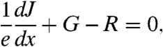
The need for appropriate device physics for organic semiconductor materials is of particular relevance to the organic bulk heterojunction solar cell (Fig. 1). In these devices, photogenerated charge pairs at the interface between donor and acceptor phases must separate and be transported to opposite electrodes in order to generate a photocurrent (2, 3). Devices made from poly(3-hexyl thiophene) (P3HT) and 6,6 phenyl C61 butyric acid methyl ester (PCBM) have achieved power conversion efficiencies of ∼5% (4) but efficiencies up to 10% are considered possible if appropriate materials and device designs can be developed (5–7). Such improvements in performance have so far been hindered by a lack of proven device design principles. Until now, drift-diffusion models based on classical semiconductor physics (8, 9) have generally been used for device simulation. However, such models fail to explain several features of the observed J-V performance, in particular the relatively strong dependence of photocurrent on bias in the operating regime, which leads to a low device fill factor. This effect has been attributed variously to an electric-field-dependent charge pair generation rate (10–12), to a light dependent parallel resistance (13), and to the effect of a superlinear dependence of recombination rate on charge density (14). In addition, in most models to date disorder has largely been ignored. However, we have previously shown that due to energetic disorder in P3HT both the bimolecular recombination coefficient and the charge carrier mobility for P3HT∶PCBM devices are carrier density dependent (15, 16), which emphasizes the importance of treating disorder when considering these and other similarly disordered devices (17).
Fig. 1.

Schematic of structure and function of P3HT∶PCBM solar cells. Light absorption results in the generation of excitons, which dissociate into electron–hole pairs at the polymer: PCBM interface. Photocurrent generation requires the transport of electrons through the PCBM phase to the cathode and of holes through the donor phase to the anode. During this transport process, photogenerated charges may approach each other and undergo bimolecular recombination to ground. The competition between charge transport and bimolecular recombination is a key consideration in this paper. TCO refers to transparent conducting oxide and PEDOT:PSS to poly(3,4-ethylene dioxythiophene):poly(styrene sulfonate).
In this paper we present an experimental methodology for determination of the empirical relationship between charge density and applied light and electrical bias in a working organic device, and we show how analysis of the data so produced reveals the nature of the optoelectronic processes that control device performance. We further show how this analysis allows the J-V curve of an organic solar cell to be predicted from experimental observation of the bias dependence of charge density and the empirical determination of a rate law for bimolecular recombination with a charge-density-dependent recombination coefficient k(n), without any fitting parameters. The analysis shows, moreover, that bimolecular recombination is sufficient to explain the observed device J-V behavior over the entire photovoltaic operational regime.
Background
In the design of organic semiconductor materials and devices, we want to be able to predict the current density–voltage (J-V) behavior of a device from details of the device structure and material parameters. The current density J in a semiconductor optoelectronic device in the steady state is controlled by the continuity equation, which relates J for electrons or holes to the volume photogeneration rate G and the volume recombination rate R. For electrons,
 |
[1] |
where e is the electronic charge and x is position. For conventional semiconductor devices, it is usual to solve Eq. 1 given functional forms for G in terms of light bias and position and for J and R in terms of charge carrier density n. The J-V response is then obtained from given relationships between the charge density at the electrodes and the potential difference V between them. In organic semiconductor devices, the functional forms for G, R, and J are, in general, not known. In particular, G is the product of photon absorption, which is influenced by optical interference on typical device length scales, and charge separation efficiency, which is a function of local phase microstructure and interfacial energetics (18). R is generally nonlinear in charge density, because of disorder in energy levels and because the organic material is not normally doped, and it is also influenced by the phase microstructure (16, 19). The current density J is again a nonlinear function of n, as a result of the charge carrier density dependence of mobility, again attributable to energetic disorder (14). Thus for organic semiconductor devices, the n dependence of the terms in Eq. 1 is, in general, not well understood and is moreover a function of the specific electronic structure and microstructure of the materials.
Determining the origin of the J-V behavior is clearly a prerequisite for improving material and device design, but requires determination of J(n), R(n), and n(V) for a given device. In this paper we present a strategy for measuring these relationships from in situ transient optoelectronic analyses of an operating organic photovoltaic device. Despite these data providing clear evidence for the presence of nonlinear effects of disorder on the electronic properties, we demonstrate that this analysis can be successfully related to a simple device model.
Results and Discussion
For the results we report herein, we employ a typical organic solar cell based upon a P3HT∶PCBM blend film, this being the most widely studied materials combination for organic photovoltaic devices, although we have already found our analysis procedure to be equally successful when applied to a range of other organic photovoltaic devices, as we discuss further below.
We have previously used charge extraction (CE) and transient photovoltage techniques to show that the open-circuit voltage of P3HT∶PCBM photovoltaic devices is primarily controlled by trap-limited bimolecular recombination of free charge carriers at the polymer: PCBM interface (15, 16). Herein, we extend our CE studies across the full range of device operating conditions between short and open circuit to determine the spatially averaged excess polaron (or electron) charge density  present in the device for a range of applied biases and different light intensities relative to dark, short circuit conditions (see Methods). Fig. 2 shows plots of
  as a function of cell voltage, V = Vapp - IRS (using a series resistance Rs = 10 Ω) (20) from V = 0 to open circuit (Fig. 2A) and as a function of light intensity over a range of 0–3 suns (Fig. 2B). The observed charge densities are too large to be assigned to electrode capacitive charge (21) and instead can be assigned to charge density in the polymer: fullerene photoactive layer generated by charge photogeneration and injection from the electrodes. This charge density will include both mobile and trapped charge in the active layer (15).
Fig. 2.

Average charge density in the device,  , as a function of (A) cell voltage at different light intensities and (B) light intensity in the range 0–3 suns for different cell voltages, where
 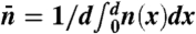 and d is the active layer thickness. In A we have also plotted the charge density present in the device under the Shockley limit, which shows that for cell voltages well below VOC the charge density is independent of voltage contrary to our observations for P3HT∶PCBM devices.
It is apparent that  is strongly dependent not only on light intensity, but also cell voltage. We note that even in the dark, the charge density in the photoactive layer increases rapidly with cell voltage, assigned, as we have discussed previously (15), to electron injection from the device electrodes. For a given light intensity, as the cell voltage is increased toward open circuit the charge density increases. As the light intensity is increased, the dependence of
  on V reduces, indicated by the reducing slope of
  against V. The continual increase of
  with V is in stark contrast to the limit of conventional, doped semiconductor devices (which we refer to as the Shockley limit) where
  remains independent of V up to within a few kBT of the open-circuit voltage VOC and then increases with a Boltzmann-like form (also shown in Fig. 2A). A dependence of
  on V at low V could result from a strong drift component to the photocurrent, or from an exponential tail in the density of states (DoS) due to intraband trap states in an energetically disordered medium that reduces the dependence of the charge carrier density at the electrodes on V (see SI Text) or both. However, the reducing slope of
  against V as light intensity increases cannot be explained by a drift current component alone and suggests a tail in the DoS, which in turn indicates energetic disorder. It is also apparent that the charge density in the dark follows a greatly reduced dependence on cell voltage when compared to a Boltzmann-like form of ndark(V), which is a further indication of strong disorder. This behavior is consistent with our previous observations that both the bimolecular rate coefficient, k, and polaron mobility measured in P3HT∶PCBM devices are strongly dependent upon charge density (15, 16, 18, 22–24) and that these dependencies can be understood in terms of trapping/detrapping dynamics in the presence of energetic disorder (25).
Consideration of the measured  data is thus clearly useful in analyzing the internal mechanisms within the device, and in particular the role of energetic disorder. Although the measurements are straightforward, no such information or analysis has previously been presented. The data immediately show that the Shockley model with linearized recombination and a Boltzmann-like dependence of n on V is not appropriate. Unlike the Shockley limit, it is clear that it is not possible to express n as the sum of light intensity and bias dependent parts. This implies that linear superposition of dark current and photocurrent is not expected to apply (see SI Text) and instead will overestimate J(V) and the fill factor. This could explain why fill factors greater than 70% are yet to be achieved for P3HT∶PCBM devices.
Now we explore whether the observed dependence of  on V and light intensity is consistent with bimolecular recombination being the dominant loss process in the device. To do this we use CE to measure
  at open circuit,
  , for each light intensity, and we use the transient photovoltage method previously reported (15, 24) to measure the bimolecular recombination rate constant k at that point. We find, as previously, a power-law dependence of k on
  of the form
 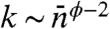 (where ϕ = 2.55 for the device studied herein). We note that our observation of a nonlinear rate law for charge carrier decay in P3HT/PCBM solar cells has recently been reproduced by two other groups, employing different experimental techniques (26, 27). Comparison with transient absorption data collected in the presence and absence of a top metal electrode has allowed us to assign the nonlinear rate law behavior to bimolecular recombination with a charge-density-dependent bimolecular recombination coefficient, k(n) (16). The power-law behavior can be explained in terms of a tail in the DoS of the polymer (25), and in P3HT∶PCBM blends, in particular, the exponent of k(n) depends upon the crystallinity of the P3HT in the photoactive layer (15, 28). Although the dependence of k on the average charge density
  does not necessarily reflect the local dependence of R on n, at open circuit the spatial variation in n can be reasonably neglected. Making this approximation, the recombination current density Jrecom becomes
| [2] |
where d is the active layer thickness and  represents the spatially averaged recombination rate. As both the charge density and recombination coefficient are influenced by charge trapping, then treating Jrecom in this manner allows the effects of disorder to also be included. In Fig. 3 we plot Jrecom as a function of
  in comparison with the measured short circuit current density at that light intensity. It is apparent that for all light intensities Jrecom ∼ Jsc (15). Given that dJ/dx = 0 at open circuit and assuming that Jsc = -eGd (i.e., all photogenerated charges are collected at short circuit), then it is apparent that
 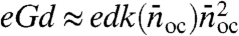 , and thus, as we have argued previously (15), that the loss of photogenerated charge carriers at open-circuit can be accounted for completely by bimolecular recombination. This result suggests that no electric field dependence of G is necessary. This observation is consistent with the observation that the polaron photogeneration yield, determined from transient absorption studies of similar devices, is independent of applied voltage (≤ 10% between 0 V and VOC) (15).
Fig. 3.

Recombination current density, Jrecom, determined from the measured charge density at open circuit and measured recombination rate at open circuit, at different bias light intensities (filled circles) and the corresponding short-circuit current (open circles) determined at the same intensities.
Now we reconstruct J(V), from short circuit to open circuit, from the measured  and knowledge of the bimolecular recombination law. Integrating Eq. 1 and assuming an electron blocking contact at the anode we have
| [3] |
Here we again apply the approximation that  (where p is the hole charge density). Although this approximation is not expected to be valid as V tends toward 0 due to spatial gradients in n under current flow, the value of the recombination term becomes negligible relative to Jsc in this limit, so the approximation can be used. The treatment implies that R depends only on
  , irrespective of the origin of the charges. This simplification is justified by our observation of the same empirical rate law under forward bias in the dark and under illumination at VOC (15, 24). We emphasize that the key assumptions of this analysis are that charge photogeneration is voltage independent and that the bimolecular recombination flux depends only upon the total charge density in the active layer of the device, independent of whether this charge is light generated or electrically injected. As we show below, the success of our analysis indicates that both assumptions are correct.
Using Eq. 3 and the  data in Fig. 2, we reconstruct the J-V curve for several different light intensities and compare with measured J(V) data in Fig. 4. The reconstructed J-V curves neglect possible contributions from alternative loss processes such as shunts and electric-field-dependent charge generation. Considering the simplicity of the model, and lack of fitting parameters, the agreement between the simulations and the experimental data is remarkable. The model gives fill factors that are within 5% of experimental values and reproduces the negative dependence of the fill factor on light intensity. In contrast to many previous analyses of such J-V curves (8, 29, 30), this analysis involves no fitting parameters but is based on independent measurements of the charge densities and recombination rates. The same procedure was applied to a range of P3HT∶PCBM-based devices, all exhibiting rate laws for bimolecular recombination, and led to excellent agreement between reconstructed and measured J-V data in each case. This agreement indicates that, at least for the annealed P3HT∶PCBM devices studied here, the shape of the J-V curve, and therefore both the device open-circuit voltage and fill factor, are primarily determined by bimolecular recombination.
Fig. 4.

Reconstruction of the J-V curve based on trap-limited bimolecular recombination. (A) Experimental J-V curves for an annealed P3HT/PCBM device under different light intensities (bold lines) compared with J-V curves reconstructed from the measured charge density data and measured bimolecular recombination law, using Eq. 3 (open circles) and (B) a comparison between the fill factors determined from both the experimental J-V curves and the reconstructed J-V curves for light intensities in the range 0.25–3.5 suns. No fitting parameters are used.
The measured and reconstructed J-V data reflect the dependence of  on V and I remarked upon in Fig. 2 above. The continual increase in
  with V leads to a steady increase in Jrecom as V increases from zero toward open circuit and thus to a subideal fill factor. The analysis thus provides a physical basis for the observed nonideal fill factor, which had previously been assigned without any detailed mechanism to a photoshunt (31, 32) or electric-field-dependent generation (29, 33). Likewise, the intensity dependence of
  leads to different fill factors at different light intensities and so to the failure of superposition as well as the elimination of a field-dependent generation term. We thus conclude that the fill factor of the J-V curve for P3HT∶PCBM devices primarily results from the direct competition between the transport of charges to the electrodes and the bimolecular recombination of opposite charge carriers during transit, and that at open circuit the charge density is sufficiently large that the recombination current completely cancels the photocurrent. For devices that have good selectivity for charge collection at the electrodes (efficient blocking layers) and do not exhibit an electric-field-dependent charge generation process, bimolecular recombination is likely to provide the fundamental limitation to the current–voltage response. Our conclusion that the fill factor for the annealed P3HT∶PCBM devices studied herein is controlled by bimolecular recombination could explain the high efficiencies that are obtainable for optimized P3HT∶PCBM solar cells (4).
We further note the bimolecular recombination coefficient k for such P3HT∶PCBM devices has been determined to be orders of magnitude lower than that expected for Langevin recombination, leading to suggestions that bimolecular recombination does not limit device performance for such devices (19). The work presented herein clearly indicates that despite the relatively low value for k, the charge densities present in the device while under operation are sufficiently large for bimolecular recombination to be the dominating loss pathway in these devices. We also highlight that contrary to current device models, our analyses do not require knowledge of the charge carrier mobilities, with our measure of charge density in effect encompassing the effect of carrier mobility. This is advantageous due to the difficulty in undertaking in situ measurements of mobility in functioning optoelectronic devices.
We have shown that bimolecular recombination losses are the primary determinant of the shape of the J-V curve for P3HT∶PCBM devices over the operating range of the device. They do not, however, have a significant impact upon device JSC. Our simulations indicate that, due to the relatively low charge densities present in the photoactive layer at short circuit, the bimolecular recombination flux is negligible under these conditions, with rather geminate (or monomolecular) recombination being the dominate loss pathway at short circuit. This conclusion is also consistent with the observation that JSC increases linearily with light intensity in such devices. Indeed, as we and others have discussed elsewhere, geminate recombination losses can be the primary determinant of charge photogeneration efficiency, and therefore JSC, in such devices (18). We conclude only that such geminate recombination losses, if present in P3HT∶PCBM devices, are not strongly dependent upon voltage or light intensity over the device operating range studied herein. It is furthermore apparent that, even for the device studied herein, the simulated J-V data slightly underestimate the loss in device current as the voltage is increased. This suggests that another voltage/light intensity-dependent loss mechanism(s) is also present. These deviations could result from a minor electric field dependence of charge generation or from light dependent leakage resulting from a photoconductive shunt pathway between partially selective device contacts. However, we emphasize that over the device operating range considered, these deviations constitute less than 10% of JSC, and thus that these additional loss pathways are not the primary determinants of the device fill factor and VOC for well optimized (annealed) P3HT∶PCBM cells.
The results shown herein were obtained from a single P3HT∶PCBM device. However, our analysis and specifically the reconstruction of the J-V curve were successfully repeated for other P3HT∶PCBM devices, including both those made in-house and externally. Moreover, we have extended these studies to other polymer/PCBM blend solar cells, including those employing the donor polymers poly(3-hexylselenophene) and the low band gap copolymer, PCPDTBT. In all cases, reconstructed J/V curves determined from the analysis reported herein were found to be in remarkably good agreement with the experimental J/V curve, suggesting that our analysis and conclusions may find applicability to a broad range of organic photovoltaic devices. Furthermore, this work may also be extendable to photovoltaic devices based on disordered inorganic semiconductors.
In this paper, we have demonstrated a previously undescribed approach to analyze the performance of organic optoelectronic devices in the presence of disorder. By focusing on empirical measurements as a function of charge density, we are able to elucidate the key features of the underlying device physics even in the presence of significant disorder, and without the use of any fitting parameters.
Methods
To determine the charge densities present in the active layer of the device we employ a simple charge extraction measurement, following procedures we have detailed previously (15). The solar cell is initially held at a fixed point on the device J-V curve, either in the dark or under illumination, and then is switched to short circuit (zero bias) while at the same time the light (if any) is switched off (24). The switch to short circuit creates a current transient as the cell discharges. When recombination losses during this charge extraction are small enough (see below), the integral of this current transient is a measurement of the excess charge in the cell under the J-V condition specified before the switching. The charge extracted will also include the charge resident on the electrodes. Thus, all CE data presented herein have been corrected for this capacitive charge using an estimate for the geometric capacitance (C = 3 nF, using ε = 3.8, d = 230 nm, and A = 0.2 cm2). Because of incurred charge carrier losses during the charge extraction transit time, the CE data provide an underestimate for the charge present in the active layer, and thus we employ an algorithm based on our studies of the charge carrier dynamics at VOC to make a correction for these charge carrier losses. Previously, we have demonstrated that the charge densities determined using charge extraction for annealed P3HT∶PCBM devices under light bias conditions are in excellent agreement with an analogous differential charging procedure (24). This provides strong support that the charge densities are correctly determined using this simple charge extraction technique. We have also previously shown that, for such devices, the charge extraction collection times are an order of magnitude faster than the corresponding carrier lifetimes (15), which indicates any charge losses due to recombination are expected to be small.
For the charge extraction studies reported herein, illumination was provided by ten 1-W white LEDs (Lumileds) with focusing optics. The lights were switched off and the device short circuited using typical metal–oxide–semiconductor field-effect transistors (on time ≤ 100 ns, Ropen ∼ 3 MΩ; Rclosed ∼ 0.5 Ω). The LEDs had intrinsic turn-off times ≤ 200 ns. Current was measured across a 13-Ω resistor in series with the cell and switch. When measuring charge at VOC, the voltage was varied by varying the light intensity. Illumination time before switching was typically 100 ms, which was enough to achieve steady state conditions while minimizing heating. When measuring charge at points on the light and dark J-V curves, the voltage was controlled using a Keithley 2400 sourcemeter. Transient photovoltage measurements were undertaken as detailed previously on the same devices employed for the CE measurements, held at open circuit as a function of bias light intensity (24).
The P3HT∶PCBM cells employed herein were prepared according to the procedure outlined elsewhere (34). The active layer, consisting of a P3HT∶PCBM-blended composite in a ratio of 1∶0.8, was blade coated from xylene solution on indium tin oxide-coated PET substrates. The active layer is sandwiched between two interface layers for blocking electrons and holes, respectively, and finished with more than 100 nm of Ag. The active layer was annealed under nitrogen at 140 °C for several minutes prior to thermal evaporation of the top electrode. Analogous data were obtained from P3HT/PCBM devices fabricated in-house, employing procedures detailed in ref. 35. Experimental measurements were performed at room temperature, illuminating through the ITO. Devices were either encapsulated or held under vacuum; device current/voltage analyses undertaken before and after data collection confirmed negligible device degradation during the course of these experiments.
Supplementary Material
Acknowledgments.
We are very grateful to Pavel Schilinsky for device fabrication and to Andrea Maurano, Christoph Brabec, and John de Mello for their valuable thoughts and discussions. We gratefully acknowledge BP Solar, the Engineering and Physical Sciences Research Council, and Konarka Technology for funding.
Footnotes
The authors declare no conflict of interest.
This article is a PNAS Direct Submission.
This article contains supporting information online at www.pnas.org/lookup/suppl/doi:10.1073/pnas.1004363107/-/DCSupplemental.
References
- 1.Borsenberger PM, Weiss DS. Organic Photoreceptors for Xerography. Boca Raton, FL: CRC Press; 1998. [Google Scholar]
- 2.McGehee MD. Overcoming recombination. Nat Photonics. 2009;3:250–252. [Google Scholar]
- 3.Campoy-Quiles M, et al. Morphology evolution via self-organization and lateral and vertical diffusion in polymer: Fullerene solar cell blends. Nat Mater. 2008;7:158–164. doi: 10.1038/nmat2102. [DOI] [PubMed] [Google Scholar]
- 4.Irwin MD, Buchholz B, Hains AW, Chang RPH, Marks TJ. p-Type semiconducting nickel oxide as an efficiency-enhancing anode interfacial layer in polymer bulk-heterojunction solar cells. Proc Natl Acad Sci USA. 2008;105:2783–2787. [Google Scholar]
- 5.Park SH, et al. Bulk heterojunction solar cells with internal quantum efficiency approaching 100% Nat Photonics. 2009;3:297–302. [Google Scholar]
- 6.Scharber MC, et al. Design rules for donors in bulk-heterojunction solar cells—Towards 10% energy-conversion efficiency. Adv Mater. 2006;18:789–794. [Google Scholar]
- 7.Ross RB, et al. Endohedral fullerenes for organic photovoltaic devices. Nat Mater. 2009;8:208–212. doi: 10.1038/nmat2379. [DOI] [PubMed] [Google Scholar]
- 8.Koster LJA, Smits ECP, Mihailetchi VD, Blom PWM. Device model for the operation of polymer/fullerene bulk heterojunction solar cells. Phys Rev B. 2005;72:085205. [Google Scholar]
- 9.Lacic S, Inganas O. Modeling electrical transport in blend heterojunction organic solar cells. J Appl Phys. 2005;97:124901. [Google Scholar]
- 10.Ooi ZE, Tam TL, Sellinger A, deMello JC. Field-dependent carrier generation in bulk heterojunction solar cells. Energ Environ Sci. 2008;1:300–309. [Google Scholar]
- 11.Blom PWM, Mihailetchi VD, Koster LJA, Markov DE. Device physics of polymer: Fullerene bulk heterojunction solar cells. Adv Mater. 2007;19:1551–1566. [Google Scholar]
- 12.Morteani AC, Sreearunothai P, Herz LM, Friend RH, Silva C. Exciton regeneration at polymeric semiconductor heterojunctions. Phys Rev Lett. 2004;92:247402. doi: 10.1103/PhysRevLett.92.247402. [DOI] [PubMed] [Google Scholar]
- 13.Riedel I, et al. Effect of temperature and illumination on the electrical characteristics of polymer-fullerene bulk-heterojunction solar cells. Adv Funct Mater. 2004;14:38–44. [Google Scholar]
- 14.Shuttle CG, Hamilton R, O’Regan B, Nelson J, Durrant JR. Measurement of charge density dependence of carrier mobility in an organic semiconductor blend. Adv Funct Mater. 2010;20:698–702. [Google Scholar]
- 15.Shuttle CG, et al. Charge extraction analysis of charge carrier densities in a polythiophene/fullerene solar cell: Analysis of the origin of the device dark current. Appl Phys Lett. 2008;93:183501. [Google Scholar]
- 16.Shuttle CG, et al. Bimolecular recombination losses in polythiophene: Fullerene solar cells. Phys Rev B. 2008;78:113201. [Google Scholar]
- 17.Novikov SV, Dunlap DH, Kenkre VM, Parris PE, Vannikov AV. Essential role of correlations in governing charge transport in disordered organic materials. Phys Rev Lett. 1998;81:4472–4475. [Google Scholar]
- 18.Clarke TM, Ballantyne AM, Nelson J, Bradley DDC, Durrant JR. Free energy control of charge photogeneration in polythiophene/fullerene solar cells: The influence of thermal annealing on P3HT/PCBM blends. Adv Funct Mater. 2008;18:4029–4035. [Google Scholar]
- 19.Pivrikas A, et al. Bimolecular recombination coefficient as a sensitive testing parameter for low-mobility solar-cell materials. Phys Rev Lett. 2005;94:176806. doi: 10.1103/PhysRevLett.94.176806. [DOI] [PubMed] [Google Scholar]
- 20. The series resistance value is determined from dark current at high applied voltages.
- 21. Using an effective dielectric constant ε = 3.8, we estimate an electrode capacitance of ∼3 nF, corresponding to a charge density at V = 0.6 V (∼VOC under 1 sun) of 2.4 × 1015 cm-3, an order of magnitude less than that observed.
- 22.Clarke T, et al. Transient absorption spectroscopy of charge photogeneration yields and lifetimes in a low bandgap polymer/fullerene film. Chem Commun. 2009:89–91. doi: 10.1039/b813815j. [DOI] [PubMed] [Google Scholar]
- 23.Ohkita H, et al. Charge carrier formation in polythiophene/fullerene blend films studied by transient absorption spectroscopy. J Am Chem Soc. 2008;130:3030–3042. doi: 10.1021/ja076568q. [DOI] [PubMed] [Google Scholar]
- 24.Shuttle CG, et al. Experimental determination of the rate law for charge carrier decay in a polythiophene: Fullerene solar cell. Appl Phys Lett. 2008;92:093311. [Google Scholar]
- 25.Nelson J. Diffusion-limited recombination in polymer-fullerene blends and its influence on photocurrent collection. Phys Rev B. 2003;67:155209. [Google Scholar]
- 26.Deibel C, Baumann A, Dyakonov V. Polaron recombination in pristine and annealed bulk heterojunction solar cells. Appl Phys Lett. 2008;93:163303. [Google Scholar]
- 27.Juska G, Genevicius K, Nekrasas N, Sliauzys G, Dennler G. Trimolecular recombination in polythiophene: Fullerene bulk heterojunction solar cells. Appl Phys Lett. 2008;93:143303. [Google Scholar]
- 28.Kim Y, et al. A strong regioregularity effect in self-organizing conjugated polymer films and high-efficiency polythiophene: fullerene solar cells. Nat Mater. 2006;5:197–203. [Google Scholar]
- 29.Lenes M, Morana M, Brabec CJ, Blom PWM. Recombination-limited photocurrents in low bandgap polymer/fullerene solar cells. Adv Funct Mater. 2009;19:1106–1111. [Google Scholar]
- 30.Waldauf C, Schilinsky P, Hauch J, Brabec CJ. Material and device concepts for organic photovoltaics: Towards competitive efficiencies. Thin Solid Films. 2004;451–452:503–507. [Google Scholar]
- 31.Schilinsky P, Waldauf C, Hauch J, Brabec CJ. Simulation of light intensity dependent current characteristics of polymer solar cells. J Appl Phys. 2004;95:2816–2819. [Google Scholar]
- 32.Waldauf C, Scharber MC, Schilinsky P, Hauch JA, Brabec CJ. Physics of organic bulk heterojunction devices for photovoltaic applications. J Appl Phys. 2006;99:104503. [Google Scholar]
- 33.Mihailetchi VD, Koster LJA, Hummelen JC, Blom PWM. Photocurrent generation in polymer-fullerene bulk heterojunctions. Phys Rev Lett. 2004;93:216601. doi: 10.1103/PhysRevLett.93.216601. [DOI] [PubMed] [Google Scholar]
- 34.Schilinsky P, Waldauf C, Brabec CJ. Performance analysis of printed bulk heterojunction solar cells. Adv Funct Mater. 2006;16:1669–1672. [Google Scholar]
- 35.Ballantyne AM, et al. The effect of poly(3-hexylthiophene) molecular weight on charge transport and the performance of polymer: Fullerene solar cells. Adv Funct Mater. 2008;18:2373–2380. [Google Scholar]
Associated Data
This section collects any data citations, data availability statements, or supplementary materials included in this article.