Abstract
A low voltage, two-level-metal, and multi-layer insulator electrowetting-on-dielectric (EWD) platform is presented. Dispensing 300pl droplets from 140nl closed on-chip reservoirs was accomplished with as little as 11.4V solely through EWD forces, and the actuation threshold voltage was 7.2V with a 1Hz voltage switching rate between electrodes. EWD devices were fabricated with a multilayer insulator consisting of 135nm sputtered tantalum pentoxide (Ta2O5) and 180nm parylene C coated with 70nm of CYTOP. Furthermore, the minimum actuation threshold voltage followed a previously published scaling model for the threshold voltage, VT, which is proportional to (t/εr)1/2, where t and εr are the insulator thickness and dielectric constant respectively. Device threshold voltages are compared for several insulator thicknesses (200nm, 500nm, and 1µm), different dielectric materials (parylene C and tantalum pentoxide), and homogeneous versus heterogeneous compositions. Additionally, we used a two-level-metal fabrication process, which enables the fabrication of smaller and denser electrodes with high interconnect routing flexibility. We also have achieved low dispensing and actuation voltages for scaled devices with 30pl droplets.
Keywords: Electrowetting, Digital microfluidics, Tantalum pentoxide, Dimensional scaling
1. Introduction
In recent years, microfluidic manipulation of liquid droplets has been widely investigated as a platform for the transport of chemical or biomedical liquids on biochips. Electrowetting-on-dielectric (EWD) is an actuator based on controlling charge at the interface of liquids and insulators over buried electrodes [1, 2]. EWD is believed to be the most feasible and efficient microfluidic actuator for lab-on-a-chip applications, as the droplets can be promptly driven to a precise position, which is not achievable by continuous flow microfluidics [3]. EWD actuators can split, mix, and dispense droplets from on-chip reservoirs, which gives more flexibility and better choices for multiple applications performed on a common platform [4–7].
EWD is a principle extended from electrocapillarity, where an electric field changes the effective surface energy between a solid insulator and a liquid interface to induce a driving force [8, 9]. EWD creates an electric field by applying a voltage at the interface between the dielectric material and a polarizable or conductive liquid droplet [7]. The electric field induces interfacial electrical charge in the liquid, which then exerts a force relative to the surface of the dielectric. Since a liquid interface is deformable, this force distorts the interface [10]. The interfacial force creates a variation in the local interfacial tension, which changes the effective contact angle [4–8, 11]. The effective contact angle changes from θ0 to θV for the applied voltage, V, and follows the Lippmann-Young equation [12]:
| (1) |
where εr is the dielectric constant of the insulator layer, ε0 is the permittivity of vacuum, γ LG is the surface tension between liquid and the filler medium surrounding to the droplet, and t is the thickness of the insulator. When actuating a droplet, opposing sets of forces act upon the droplet: an electrowetting force induced by the electric field and resistant forces that include drag forces caused by interactions with the filler medium and contact line friction [13]. At the moment the droplet is actuated, the electrowetting force is balanced with the sum of all drag forces. The minimum voltage applied to achieve this effect is defined as the threshold voltage, VT [1]:
| (2) |
where α is the contact hysteresis angle. Since the surface tension and the contact hysteresis angle are influenced by the filler medium and the hydrophobic material, the threshold voltage is variably determined by the dielectric-thickness-to-dielectric-constant ratio, (t/εr)1/2. Thus, to reduce the actuation threshold voltage, it is required to reduce t/εr.
In order to reduce the actuation threshold voltage of EWD devices, sub-micrometer thin films and high dielectric constant materials were used in the fabrication process. In the past EWD devices were fabricated with thick, low dielectric constant fluoropolymer insulators, such as 800nm of parylene C [8], for which actuation voltages were higher than 60V. For reduced threshold voltage operation, high dielectric constant materials, such as barium strontium titanate ( (Ba,Sr)TiO3, BST) [14], tantalum pentoxide (Ta2O5) [15], and aluminum oxide (Al2O3) [16] have been tested as insulators on EWD devices. Al2O3 was claimed to actuate droplets at 3V but with a velocity below 1µm/s. However, 9V was acquired to move droplets to a neighboring electrode within 1s (1Hz switching rate). Both previously reported BST and Ta2O5 EWD devices demonstrated a 1Hz switching actuation threshold of 15V. However, the BST and Al2O3 devices only demonstrated droplet transport, and the Ta2O5 device was only able to dispense with a syringe providing pressure. The most difficult operation for EWD devices is dispensing droplets from a closed, on-chip reservoir without external pressure assistance, which requires more force and hence higher voltage than transporting droplets. It is also required that dielectric breakdown and insulator charging at these higher voltages not occur to avoid major reliability problems.
In this work, the lowest dispensing voltage achieved was 11.4V to split a 300pl droplet from a 140nl reservoir with 100µm electrodes and a 20µm gasket layer. The actuation threshold voltage of EWD devices made with a multilayer insulator was 7.2V at 1Hz switching rate. A threshold voltage scaling model [1] is verified with single layers of different thicknesses of parylene C and Ta2O5. In addition, multilayer insulator devices were fabricated with stacked parylene C and Ta2O5 films for improved reliability. The multilayer insulators were also found follow the scaling model. Scaling of the physical dimensions is also demonstrated with a two-level-metal structure in a device capable of dispensing 30pl droplets onto 35µm electrodes with a 10µm thick gasket.
2. Material and Methods
2.1 High dielectric constant material
Parylene C (εr ≅ 3) and silicon dioxide (SiO2, εr ≅ 3.7) have been the most frequently used materials for EWD actuators [4, 5]. The actuation threshold voltages have been reported to be 60~80V for 800nm parylene C and a 60nm Teflon hydrophobic layer [7, 8] and 25V for 100nm silicon dioxide and 20nm Teflon [5]. The higher voltages needed for operations such as dispensing and splitting have previously prohibited the use of ultra-thin insulators, as they are more susceptible to electrical breakdown and poor reliability. Thus, the use of high dielectric constant materials becomes another solution to reduce EWD applied voltage. The gate oxide in MOSFETs presents similar issues with regard to insulator breakdown and reliability, so those materials used in CMOS devices are potential solutions for EWD devices. Silicon nitride, Si3N4 (ε r ≅ 8), barium strontium titanate, (Ba,Sr)TiO3 (BST, εr ≅ 180), aluminum oxide, Al2O3 (εr ≅ 10), and tantalum pentoxide, Ta2O5 (εr ≅ 20 ~ 25), have been tested as insulator layers on EWD devices. Since the dielectric constant of Si3N4 and Al2O3 is two to three times that of SiO2, the threshold voltage reduction is by a factor , which was not considered to be a significant enough improvement. On the other hand, devices with 1mm × 1mm electrodes coated with 70nm BST films deposited by metal-oxide chemical vapor deposition (MOCVD) [14] and 95nm anodic Ta2O5 films [15] both reached the relatively low threshold voltage of 15V. Both materials were coated with a thin fluoropolymer film.
For example, since BST has a very high dielectric constant with a thin 100nm film (t/εr=100nm/180), the ratio of effective insulator thickness to dielectric constant is much smaller than a 70nm hydrophobic layer (t/εr=70nm/2), and can be neglected. This is also the reason why the actuation voltage of Moon et al. [14] is the same as Li et al. [15], but using the thinner and higher dielectric constant material. I.e. even in the same structure, the higher dielectric constant material may not result in lower actuation voltage, and it depends on the film thickness and the hydrophobic layer’s properties.
The onset of charge trapping has been proposed to occur when the effective dielectric strength of the fluoropolymer layer, DFP, is exceeded [17]. Thus the threshold voltage for the onset of charge trapping in a two-layer film is given by the expression:
| (3) |
where ε and t are the dielectric constant and thickness of each material, and FP, 1, and 2 represent the fluoropolymer layer and insulators beneath. When the applied voltage is higher than the voltage limit of Eq. (3), trapping of charges at the surface occurs and higher voltages are then required to achieve similar droplet actuation due to a shift in the threshold voltage. As a result, when the high dielectric constant insulator is relatively thin, the hydrophobic layer, for which the dielectric constant is relatively low, dominates the factor t/εr. Most of the voltage drop is across the hydrophobic layer, and higher voltage applied with this thin film would cause it to breakdown more easily. Even though the previously reported threshold voltage values were as low as 15V, the reliability of these EWD devices was limited by factors such as leakage current and time-dependent dielectric breakdown [14].
Among the materials tested, the dielectric constants of Al2O3 and Si3N4 are too low for practical use. For BST, the dielectric constant is so high for thin films that this layer’s effective t/εr ratio is negligible compared to the hydrophobic layer, which becomes the major contributor to the insulator stack. This results in most of the voltage drop occurring across the hydrophobic layer, and causes devices to break down more easily. Thus, one would expect that BST devices could not easily dispense droplets, due to the higher voltage required for dispensing operations. Therefore, the final choice was Ta2O5, which has been widely evaluated as the gate oxide in the semiconductor industry because of its high dielectric constant and dielectric strength (~8MV/cm) [18]. Multiple techniques are available to deposit this material, such as evaporation, sputtering, anodic oxidation of tantalum, pulsed laser deposition, and chemical vapor deposition (CVD) [19]. In this study, Ta2O5 was deposited by a RF dielectric sputtering system with a 99.99% Ta2O5 target. The deposition power was set at 200W and the deposition pressure was set at 13mTorr with 10% oxygen in the chamber, producing a deposition rate of 0.9nm/min. Testing was performed with a sandwich electrode-insulator-electrode structure, from which the dielectric constant for the 200nm Ta2O5 film was determined to be approximately 23. Numerous reports have shown that post deposition treatment with an annealing process improves the electrical properties of tantalum pentoxide films prepared by the sputtering method [18–21]. These reports describe various annealing procedures which were performed after deposition, resulting in variations in surface structure, dielectric constant, dielectric strength, and leakage current. Here, EWD chips were annealed by a rapid thermal anneal system (RTA, Jipelec JetFirst 100), a photonic heating system, at 400°C in a N2 atmosphere (200sccm) for 10 minutes. We found that annealing only slightly influenced the dielectric constant and dielectric strength, but notably EWD devices appeared to function with the same reliability with or without the annealing procedure.
2.2 Device Fabrication
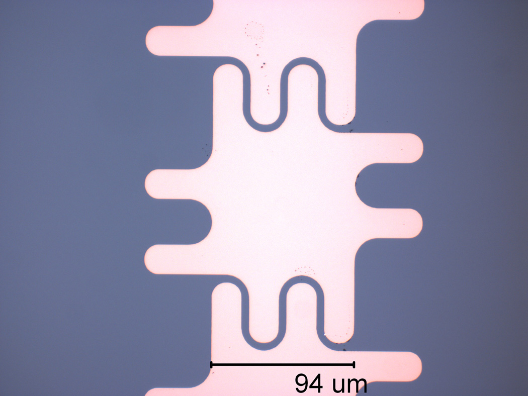
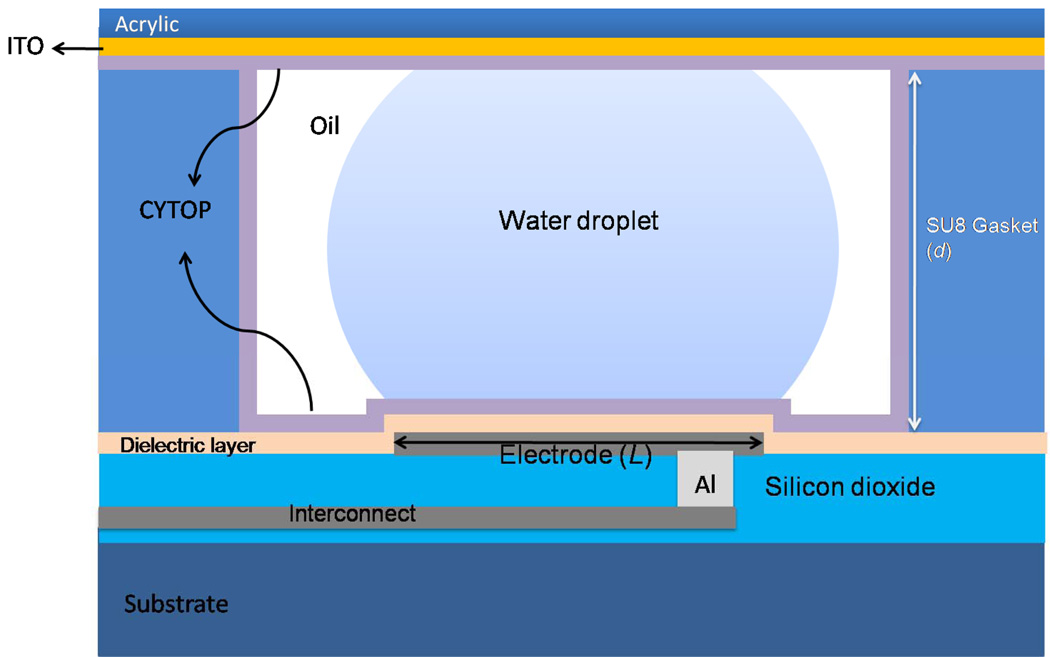
A two-level-metal device design was developed to provide the capability of fabricating smaller and denser electrodes with interconnect routing flexibility. The electrodes were designed with a pitch (L) of 100µm with 20µm round interlocking shapes (shown in Fig. 1), and spacing between electrodes of 5µm. Interlocking fingers facilitate droplet electrowetting by adjacent electrodes. A second device was designed with dimensionally-scaled electrodes having a pitch of 35µm and spacing between electrodes of 3µm. The EWD device cross-section is illustrated in Fig. 2. The devices were fabricated on 2cm ×3cm silicon wafer pieces coated with 150nm of SiO2 as a bulk insulation layer. Then, the first layer of 100 nm Cr for the electrode connections was applied and patterned by wet etching, followed by deposition of a 1µm layer of PECVD SiO2. Via holes were next etched with a buffered oxide etch and filled with patterned sputtered aluminum. The second layer of 100nm Cr for the electrodes and pads was applied and patterned. Varying thicknesses of Ta2O5 were sputtered, after which an SU-8 gasket was spun on the wafer and developed. When using parylene C as the dielectric layer, different thicknesses were coated after the gasket was formed. The SU-8 gasket thickness (d) was dependant on the electrode pitch, and was determined by the desired d/L ratio of approximately 0.2 [1, 7, 8]. For some devices the gasket was 20µm thick with L = 100µm, while other devices were fabricated with 10µm thick gaskets and L = 35µm. Finally, the hydrophobic layer, composed of 70nm CYTOP, was spun on the wafers at 3000rpm, then annealed on a hot plate at 110°C for 1min, after which the devices were placed in a vacuum desiccator for 24hr. Holes of approximately 500µm in diameter were drilled in an acrylic top plate at the location of the reservoir inlets to inject liquid into the reservoirs. This top plate was sputtered with 100nm indium-tin-oxide (ITO) to ground the droplets, and a similar 70nm CYTOP layer was applied over the ITO. The devices were tested with DI water with red food dye or with a standard buffer. The chips used a filler medium of 1.5cSt silicone oil with 2% surfactant.
Figure 1.
Electrode design with symmetric interlocking fingers, which are 35µm long and 20µm wide, rounded at the edges and corners.
Figure 2.
Cross sectional view of a two-level-metal EWD device. (Not to scale.)
2.3 Control and Detection
EWD chips were tested with a 32-channel relay controller board (National Control Devices, LLC) connected to an USB port on a computer, and controlled by a custom program with which we can either manually or programmatically actuate droplets. The input voltage to the electrodes was applied by either a DC or an AC voltage source. AC power (1k Hz sine waves) was produced with a function generator (Agilent 33250A) connected to a 10× voltage amplifier (FLC F10A). A CCD camera (Basler avA1000-120kc) was mounted on a viewing microscope to capture videos of droplet motion on the device.
3. Results and Discussion
3.1 Voltage Scaling
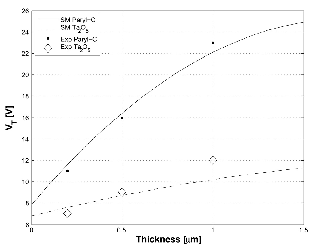
Because the contact hysteresis angle (α) and surface tension (γ LG) in Eq. (2) of water droplets in a silicone oil medium are lower than those in an air medium, the EWD device threshold voltage in silicone oil is smaller than in air, thereby allowing for a larger operating voltage range in oil [1]. The scaling model curves, according to Eq. (2), for parylene C and Ta2O5 in silicone oil with different thicknesses are plotted in Fig. 3. Threshold voltage model parameters used in these calculations are α = 4°, γLG= 47mN/m, θVT = 104°, θ0 = 125° [22], and εr ≅ 3 for parylene C or εr ≅ 23 for Ta2O5.
Figure 3.
Threshold voltages for different dielectric thickness. Scaling models results for CYTOP on parylene C and CYTOP on Ta2O5 in silicone oil are plotted according to Eq. (2).
Different thicknesses (0.2, 0.5, and 1µm) of each material were deposited on the electrode arrays followed by formation of a 70nm layer of CYTOP, and the resulting threshold voltages were measured. The measured data are in reasonable agreement with the square root of thickness dependence in Eq. (2), considering that the relative influence of the 70nm CYTOP layer as a variable. However, since εr ≅ 3 for parylene C and the dielectric constant of CYTOP is approximately 2, the CYTOP has little influence on the overall dielectric behavior of this insulator. On the other hand, for Ta2O5, the dielectric constant is 23, and CYTOP is no longer only a hydrophobic layer, but also an insulator which dominates the t/εr term. As a result, the threshold voltage improvement from the use of Ta2O5 is not as effective as parylene C for the same thickness decrease. Whereas the magnitude of the threshold voltage data agree reasonably well with scaling model calculations, the data do not exactly follow the (t/εr)1/2 dependence predicted by the scaling model.
3.2 Multi Layer Insulators
Tantalum pentoxide films can significantly decrease the actuation threshold voltage, but experimental work has shown reduced reliability in these devices. When the devices are operated over the course of 100 cycles, the droplet motion often slows or even stops. Increased voltage is required to actuate the droplet at the same rate, continually decreasing the device’s useful lifetime. This phenomenon is believed to be caused by the insulator accumulating charges at the surface after several operations. The thicker the dielectric layer, especially with Ta2O5, the more obvious the effect. As the required actuation voltage increases due to charging, the dielectric layer eventually experiences catastrophic breakdown. The most probable explanation is that pin-holes at the dielectric, may allow the liquid to come in contact with the electrode, causing electrolysis. Although annealing may reduce this problem, breakdown was still observed for 200nm Ta2O5 devices at 18V. Parylene C is a polymer material commonly used as a moisture barrier [23], and the dielectric strength is 2MV/cm for films thicker than 2µm [24]. However, for the 200nm film, the pin-holes problem is more serious than for films in the micron range, and the parylene C breaks down at approximately 35V.
Multiple layer insulators can combine the benefits from the two material layers and reduce their disadvantages. In one set of experiments, a 135nm film of Ta2O5 was deposited on a device wafer followed by a 450nm film of parylene C and 70nm of CYTOP. By applying Ta2O5 layer first, the parylene C acts to cover any pinholes in that layer for more complete coverage, while retaining a portion of the high dielectric constant and strength of the Ta2O5. Testing of the finished devices showed the threshold voltage to be 18V and the breakdown voltage greater than 50V. The actuator could dispense 300pl droplets from the 140nl reservoirs with as low as 20V, which was much lower than the breakdown voltage. Dispensing sequence images are shown in Fig. 4. Further reducing the insulator thickness to 135nm Ta2O5 and 180nm parylene C decreased the threshold voltage to 7.2V and the dispensing voltage to 11.4V. These are the lowest operating voltages in a usable system reported to date, and the breakdown voltage for this structure was 55V. The comparison of actuation voltages and breakdown voltages for each structure is presented in Table 1. When the thickness of parylene C was lower than 100nm, the coverage of this film would be inadequate. With high dielectric constant Ta2O5, the ratio of effective insulator thickness to dielectric constant is lower than parylene C, so we deposited Ta2O5 underneath parylene C to improve the breakdown voltage but did not significantly increase the actuation voltage.
Figure 4.
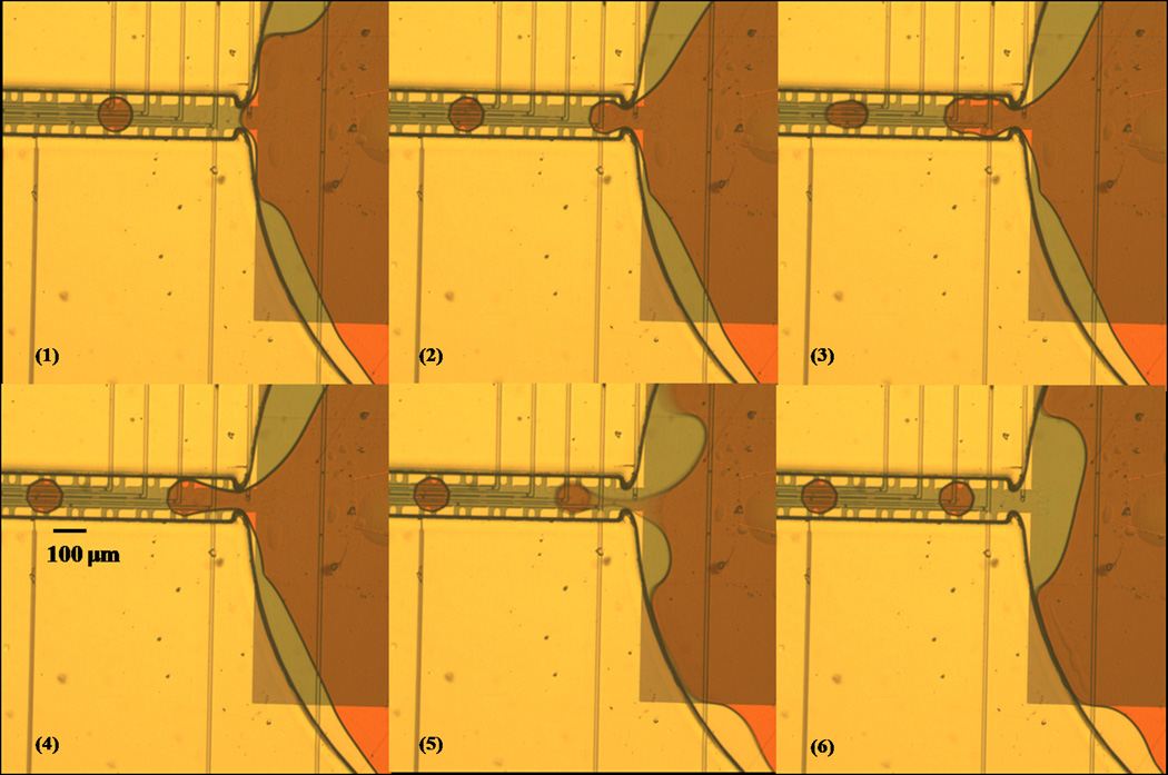
Image sequence of droplet dispensing. 300pl droplets were dispensed from a 140nl reservoir on 100µm electrodes. The channel is 150µm in width and 20µm in height with a 100µm wide curved neck which fit the liquid protrusion and helped to pull out the liquid. The electrodes in the channel were turned on in sequences to pull the liquid out from the reservoir, shown from (1) to (4). The reservoir electrode was turned on to split the droplet in (5) and all electrodes were then turned off after dispensing was completed.
Table 1.
Comparison of different structure combination. Multi layer structure with Ta2O5underneath parylene C could severely improve the breakdown voltage and did not significantly increase the actuation voltage.
| Device Structure | Effective Capacitance (t/εr)1/2 |
Actuation Threshold Voltage |
Breakdown Voltage |
|---|---|---|---|
| 200nm Parylene C/70nm CYTOP | 0.316 (µm)1/2 | 11V | 35V |
| 200nm Ta2O5/200nm Parylene C/70nm CYTOP | 0.330 (µm)1/2 | 10V | 70V |
| 120nm Ta2O5/200nm Parylene C/70nm CYTOP | 0.325 (µm)1/2 | 10V | 60V |
| 200nm Ta2O5/100nm Parylene C/70nm CYTOP | 0.275 (µm)1/2 | 8V | 26V |
| 200nm Ta2O5/70nm CYTOP | 0.205 (µm)1/2 | 6V | 18V |
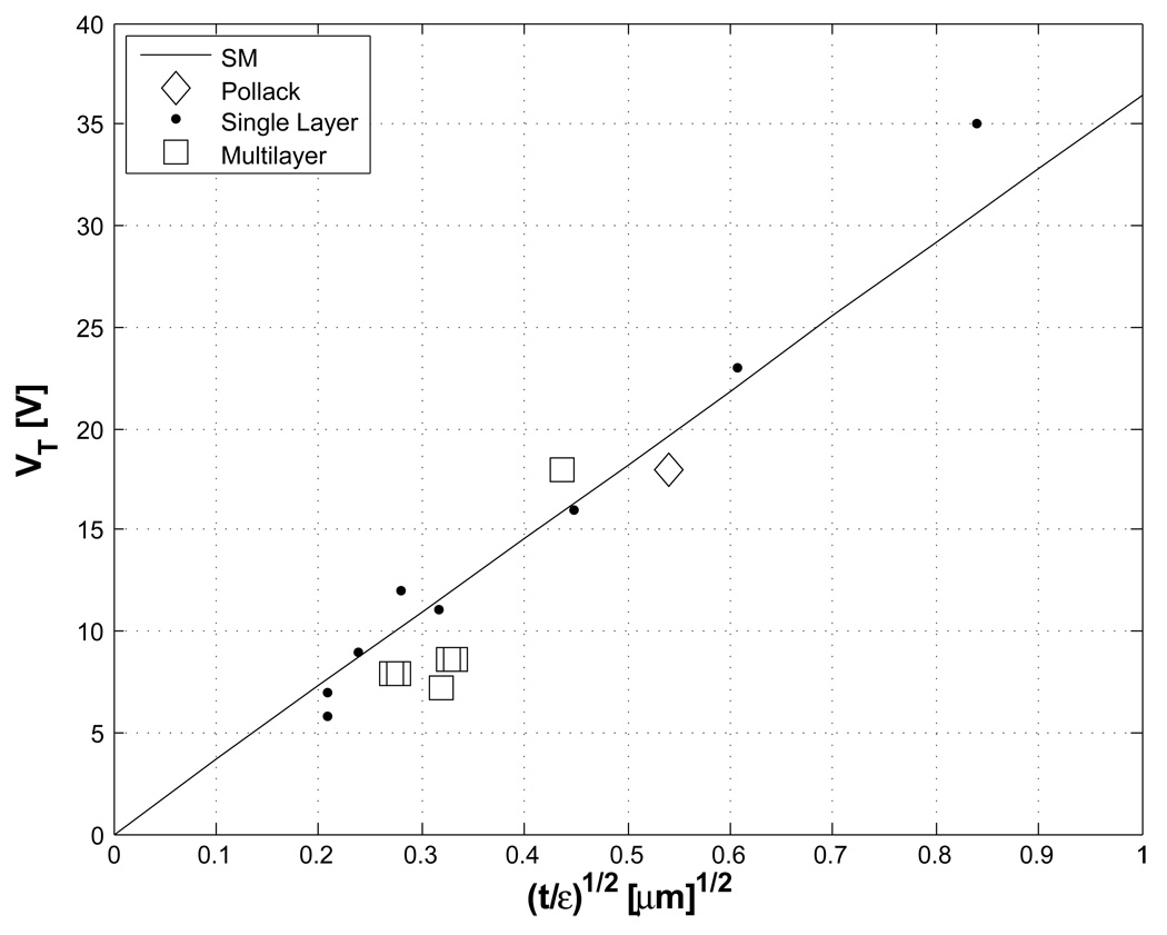
In order to compare the scaling model to experimental results from the single and multilayer materials, the threshold voltage is plotted against (t/εr)1/2 in Fig. 5. Experimental results, including the previous reports [7, 8], indicate that the scaling model is still valid even with multilayer insulators.
Figure 5.
Threshold voltage scaling with the ratio of insulator thickness and dielectric constant. The linear line is the scaling model in silicone oil, and experimental results including single layer insulators and multi layer insulators follow with the model trend.
3.3 Device Layout
With a two-level-metal process interconnects were routed on the lower level, which was insulated from the top level electrodes by a 1µm silicon dioxide film. By burying the interconnecting wires beneath the electrodes, electrowetting is restricted to only the electrode, and the footprint of the device can be made more compact while allowing more flexibility in the electrode layout. For the 100µm EWD device, most of the 200 electrodes could be bused together and controlled by 22 isolated leads. The smaller-scale device consisted of 4 × 45 electrodes arrays with 35µm pitches, 10µm thick SU-8 gaskets, and 3µm gaps between electrodes. Reservoirs were designed to hold 160nl. These smaller devices were fabricated with 200nm Ta2O5 and 200nm parylene C, and 70nm CYTOP. Droplets of 30pl volume were dispensed from a reservoir at 30V and actuated across the chip at 13V. Images of the dispensing sequences are shown in Fig. 6.
Figure 6.
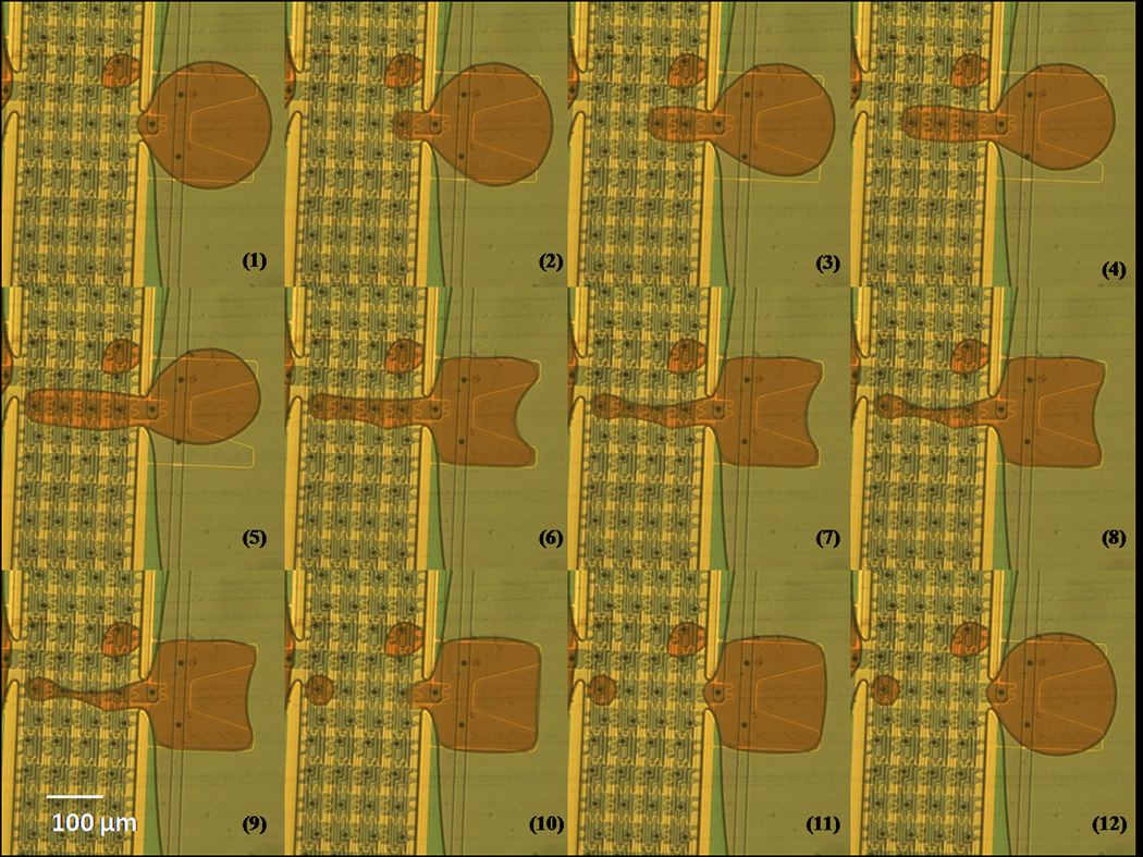
Dispensing sequence images. A 30pl droplet was successfully dispensed from a reservoir. From (1) to (5), the electrodes in the channel were turned on in sequences to pull out the liquid. In (5), only the most left electrode was on, and then the reservoir electrode was also turned on in (6) ~ (10) to split the droplet from the reservoir. The electrodes were then all turned off after dispensing.
4. Conclusions
Experimental EWD devices with 100µm electrode pitch were fabricated with an actuation threshold voltage of 7.2V and a dispensing voltage of 11.4V. These operational voltages are much lower than the dielectric breakdown voltages of the electrode insulator. As a result, these devices can be used repeatedly with more reliability. Multi layer insulator devices deposited with a 135nm Ta2O5 and 180nm parylene C were fabricated and found to be more robust and better able to operate under lower applied voltages than the devices made with a homogeneous single dielectric layer. The experimental results obtained in this study verify the prediction of a threshold voltage scaling model [1], in that the observed threshold voltages for all of the studied devices follow the trends outlined by the model. In addition, physical dimension scaling was demonstrated. The two-level-metal structure increases the flexibility in electrode design, allowing denser and smaller electrodes to be integrated on the devices. With an electrode size of 35µm, the EWD devices were able to dispense 30pl droplets from on-chip reservoirs. These results show the capability of scaling not only actuation threshold voltages, but also physical dimensions, to the extent that the minimum size limits have yet to be reached.
Acknowledgements
This research was supported by Grant # R01 HG 004354-01 from the National Institute of Health and Grant CMMI-0700021 from the National Science Foundation.
Biographies
Yan-You Lin received his B.S. degree in Electronics Engineering from National Chiao Tung University, Taiwan in 2004, and M.S. degree in Electrical Engineering from National Taiwan University, Taipei, Taiwan, in 2006. He is currently working toward Ph.D. degree in Electrical and Computer Engineering at Duke University, Durham, North Carolina. His research interests include microfluidics, lap-on-a-chip technologies, and microsystems design.
Randall Evans is a Ph.D. Candidate at Duke University in Electrical and Computer Engineering. His work largely involves fabrication process engineering in Duke’s cleanroom for digital microfluidics as well as the design and test of devices used to print a tissue engineering scaffold embedded with cells, with a designed vascular network as a part of the scaffold. He also enjoys racquetball and origami.
Erin Ferguson Welch received her PhD in Analytical Chemistry from the University of North Carolina at Chapel Hill in 2009. She is currently a postdoctoral fellow in Electrical and Computer Engineering at Duke University, with interests in general microfluidics, digital electrowetting, DNA sequencing and analysis.
Bang-Ning Hsu received the B.S. degree in Applied Chemistry from National Chiao Tung University, Hsinchu, Taiwan, in 2004 and the M.S. degree in Electrical and Computer Engineering from Duke University, in 2010. He is currently pursuing the Ph.D. degree in Electrical and Computer Engineering at Duke University. His research focuses on aerosol analysis on digital microfluidic platforms.
Andrew C. Madison received the B.S. degree in Biology and Chemistry, in 2007, and the M.S. degree in Engineering Physics, in 2009, both from Appalachian State University in Boone, NC. He is currently working towards the Ph.D. degree in Electrical and Computer Engineering at Duke University. His research interests include the development of chemical and photonic sensing strategies in digital microfluidic systems dedicated for use in medical diagnostics.
Richard B. Fair is Lord-Chandran Professor of Engineering at Duke. His current research areas include digital microfluidic devices, applications, and technology. He has published over 150 papers in refereed journals and conference proceedings, written 11 book chapters, edited nine books or conference proceedings, and given over 130 invited talks. Dr. Fair is also a Fellow of the IEEE, a Fellow of the Electrochemical Society, past Editor-in-Chief of the Proceedings of the IEEE, and he has served as Associate Editor of the IEEE Transactions on Electron Devices. He is a recipient of the IEEE Third Millennium Medal (2000) and the 2003 Solid State Science and Technology Prize and Medal from the Electrochemical Society, which was presented in Paris.
Footnotes
Publisher's Disclaimer: This is a PDF file of an unedited manuscript that has been accepted for publication. As a service to our customers we are providing this early version of the manuscript. The manuscript will undergo copyediting, typesetting, and review of the resulting proof before it is published in its final citable form. Please note that during the production process errors may be discovered which could affect the content, and all legal disclaimers that apply to the journal pertain.
Reference
- 1.Song JH, Evans R, Lin Y-Y, Hsu B-N, Fair RB. A scaling model for electrowetting-on-dielectric microfluidic actuators. Microfluid Nanofluid. 2009;7:75–89. [Google Scholar]
- 2.Fair RB. Digital microfluidics: is a true lab-on-a-chip possible? Microfluid Nanofluid. 2007;3(3):245–281. [Google Scholar]
- 3.Tabeling P. Introduction to microfluidics. New York: Oxford University Press; 2005. [Google Scholar]
- 4.Cho SK, Fan S-K, Moon H, Kim C-J. Towards digital microfluidic circuits: creating, transporting, cutting and merging liquid droplets by electrowetting-based actuation. IEEE Int. Conf. MEMS. 2002;11:454–461. [Google Scholar]
- 5.Cho SK, Moon H, Kim C-J. Creating, Transporting, Cutting, and Merging Liquid Droplets by Electrowetting-Based Actuation for Digital Microfluidic Circuits. J. Microelectromech. S. 2003;12(1):70–80. [Google Scholar]
- 6.Pollack MG. Thesis (Ph D ) Duke University; 2001. Electrowetting-based microactuation of droplets for digital microfluidics. [Google Scholar]
- 7.Pollack MG, Shenderov AD, Fair RB. Electrowetting-based actuation of droplets for integrated microfluidics. Lab. Chip. 2002;2:96–101. doi: 10.1039/b110474h. [DOI] [PubMed] [Google Scholar]
- 8.Pollack MG, Fair RB, Shenderov AD. Electrowetting-based actuation of liquid droplets for microfluidic applications. Appl. Phys. Lett. 2000;77(11):1725–1727. [Google Scholar]
- 9.Lippmann MG. Relations entre les phénomènes electriques et capillaires. Ann. Chim. Phys. 1875;5(11):494–549. [Google Scholar]
- 10.Berthier J. Microdrops and digital microfluidics. Norwich, NY: William Andrew Publish; 2008. [Google Scholar]
- 11.Lee J, Moon H, Fowler J, Schoellhammer T, Kim C-J. Electrowetting and electrowetting-on-dielectric for microscale liquid handling. Sensosr Actuator A-Phys. 2002;95 [Google Scholar]
- 12.Berge B. Electrocapillarite et mouillage de films isolants par l'eau. C R Acad. Sci. 1993;317(2):157–163. [Google Scholar]
- 13.Ren H, Fair RB, Pollack MG, Shaughnessy EJ. Dynamics of electrowetting droplet transport. Sensosr Actuator B-Chem. 2002;87:201–206. [Google Scholar]
- 14.Moon H, Cho SK, Garrell RL, Kim C-J. Low voltage electrowetting-on-dielectric. J. Appl. Phys. 2002;92(7):4080–4087. [Google Scholar]
- 15.Li Y, Parkes W, Haworth LI, Stokes AA, Muir KR, Li P, Collin AJ, Hutcheon NG, Henderson R, Rae B, Walton AJ. Anodic Ta2O5 for CMOS compatible low voltage electrowetting-on-dielectric device fabrication. Solid State Electron. 2008;52:1382–1387. [Google Scholar]
- 16.Chang J-h, Choi DY, Han S, Pak JJ. Driving characteristics of the electrowetting-on-dielectric device using atomic-layer-deposited aluminum oxide as the dielectric. Microfluid Nanofluid. 2009;8:269–273. [Google Scholar]
- 17.Berry S, Kedzierski J, Abedian B. Irreversible electrowetting on thin fluoropolymer films. Langmuir. 2007;23:12429–12435. doi: 10.1021/la7017743. [DOI] [PubMed] [Google Scholar]
- 18.Chaneliere C, Autran JL, Devine RAB, Balland B. Tantalum pentoxide (Ta2O5) thin films for advanced dielectric applications. Mater. Sci. Eng. 1998;R22:269–322. [Google Scholar]
- 19.Itoh E, Maki K, Miyairi K. Effect of annealing on dielectric dispersion of tantalum oxidefilms prepared by RF sputtering. Ann. R. CEIDP. 1999;1:62–65. [Google Scholar]
- 20.Corbella C, Vives M, Pinyol A, Porqueras I, Person C, Bertran E. Influence of the porosity of RF sputtered Ta2O5 thin films on their optical properties for electrochromic applications. Solid State Ionics. 2003;165:15–22. [Google Scholar]
- 21.Cho S-D, Paik K-W. Study on the amorphous Ta2O5 thin film capacitors deposited by dc magnetron reactive sputtering for multichip module applications. Mater. Sci. Eng. 1999;B67:108–112. [Google Scholar]
- 22.Srinivasan V, Pamula V, Rao KD, Pollack MG, Izatt JA, Fair RB. 3-D imaging of moving droplets using optical coherence tomography. 7th Int. Conf. Chem. Biochem. S. 2003 [Google Scholar]
- 23.Noh H-S, Moon K-S, Cannon A, Hesketh PJ, Wong CP. Wafer bonding using microwave heating of parylene intermediate layers. J. Micromech. Microeng. 2004;14(4):625–631. [Google Scholar]
- 24.Pang C, Gham JG, Nenadic Z, Musallam S, Tai Y-C, Burdick JW, Andersen RA. A new multi-site array with monolithically integrated parylene flexible cable for neural prostheses. 27th IEEE Eng. Med. Biol. Soc. Ann. 2005 doi: 10.1109/IEMBS.2005.1616146. [DOI] [PubMed] [Google Scholar]


