Abstract
This paper reports a new type of diffractive microlens based on finite-areas of 2D arrays of circular nanoholes (patches). The plasmonic microlenses can focus single wavelengths of light across the entire visible spectrum as well as broadband white light with little divergence. The focal length is determined primarily by the overall size of the patch and is tolerant to significant changes in patch substructure, including lattice geometry and local order of the circular nanoholes. The optical throughput, however, depends sensitively on the patch substructure and is determined by the wavelengths of surface plasmon resonances. This simple diffractive lens design enables millions of broadband plasmonic microlenses to be fabricated in parallel using soft nanolithographic techniques.
Microlenses play many important roles in micro-optoelectronics,1 from coupling light into single mode waveguides2 to collimating emission from laser diodes3 to displaying images in three dimensions.4, 5 Although refractive microlenses are extensively used in commercial devices, chromatic and spherical aberrations1, 6 restrict their range of application. In contrast, diffractive lenses (known as micro-Fresnel lenses) exhibit less aberration; however, their physical size7, 8 and complex 3D surface profiles limit their use in miniaturized and highly scaled devices because the micro-circuitry fabrication requires precise alignment among multiple lithographic steps.9
Surface plasmons, collective charge oscillations on a metal surface, provide opportunities to reduce the size of optical elements by strong confinement of electromagnetic radiation.10-12 Optical components composed of plasmonic materials exhibit enhanced optical transmission,13-15 nanoscale waveguiding,16-18 and light generation in subwavelength volumes.19-21 The principles of diffraction from nanostructured surfaces have been used to control the coupling of light into and out of surface plasmon modes10 and have also been applied to design plasmonic lenses with subwavelength features. Plasmonic microlenses reported previously, however, have required that their substructure (usually nanoslits) be fabricated with variations in size such that each aperture transmitted light with a different phase delay.22-26
Here we report how finite-areas of two-dimensional (2D) arrays of plasmonic nanoholes can function as broadband microlenses. Patches of circular nanoholes focused single wavelengths of light across the entire visible spectrum as well as broadband white light with minimal divergence. Different from other plasmonic lenses that require precisely designed substructure to operate at specific wavelengths, patches exhibit focusing characteristics that are mostly independent of lattice geometry. We found that the focal length was defined primarily by the overall diameter of the patch but that the optical throughput was determined by the surface plasmon resonances of the patch substructure. The discovery that plasmonic diffractive microlenses can exhibit robust focusing properties that are highly tolerant of substructure opens opportunities to generate large-area arrays using massively parallel nanofabrication methods.
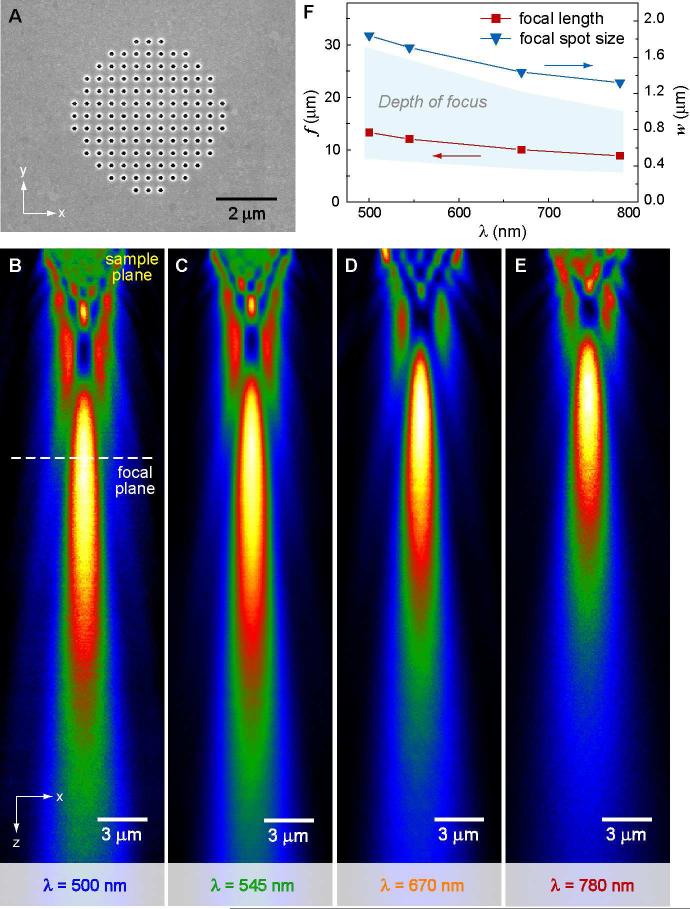
Figure 1 depicts the focusing properties of a 2D finite array (patch) of plasmonic nanoholes. A 5-μm diameter patch having circular nanoholes arranged in a square lattice was prepared by focused ion beam (FIB) milling of a 180-nm thick Au film on a glass substrate. All the holes had the same diameter and were on a pitch a0 = 400 nm (Fig. 1A). Confocal scanning optical microscopy22 was used to map the 3D optical fields generated from plane waves incident on individual patches. Under collimated, unpolarized light at an operating wavelength λ = 500 nm, a well-defined focal spot (location of maximum intensity) was observed in the xz plane through the center of the patch at z = 13.3μm (Fig. 1B). The focal spot is subject to the classical diffraction-limit because far-field focusing does not originate from evanescent field recovery23 or superoscillations.24, 27 The FWHM of the spot (at the focal plane) was 1.83μm (Fig. S1), which is smaller than the focal spot from a 2D array of spatially varying apertures.25 Multiple orders of maxima resembling characteristic diffraction patterns from a Fresnel zone plate were observed even though the nanoholes within a patch—unlike the substructure within a diffractive lens—were uniformly spaced and had the same size. Also, the periodic lattice generated checkerboard optical patterns in the region close to the Au film (<10μm) that are attributed to the Talbot effect, a self-imaging phenomenon exhibited by infinite 2D nanohole arrays.28 This diffraction pattern was not present beyond the near-field region because of the finite size of the nanohole arrays.
Figure 1. Patches of plasmonic nanoholes can focus over a range of different wavelengths.
(A) SEM image of a 5-μm patch of nanoholes with the same size and shape. The circular nanoholes are 150-nm in diameter and a0 = 400 nm. (B)-(E) Confocal scanning optical images of the patch at λ = 500 nm, 545 nm, 670 nm and 780 nm (x-z plane scanning area = 10 × 40 μm2). (F) Over the visible spectrum, the change of the focal length was smaller than the depth of the focus.
Similar to other diffractive lenses,29 the focal spot size (w) of the patch decreased slightly when the incident wavelength increased (Fig. S1). Hence, a focal spot of higher quality (smaller ratio of spot size to wavelength) can be achieved at longer wavelengths (Figs. 1C-1E). The dependence of focal length on operating wavelength λ of a patch can be expressed by a relation derived from the Rayleigh-Sommerfeld integral for a circular aperture with radius ρ:30
| (1) |
where I is intensity, A0 is the maximum intensity, and z is the distance from the aperture. The calculated focal lengths are 12.5, 11.5, 9.3 and 8 μm for a 5-μm patch at λ = 500, 545, 670 and 780 nm, respectively; all values are in good agreement with Figs. 1B-E. Notably, the shift of the focal length was much smaller than the depth of focus over all wavelengths (Fig. 1F), which suggests that patches can act as broadband plasmonic microlenses with a common focusing region throughout the entire visible range.
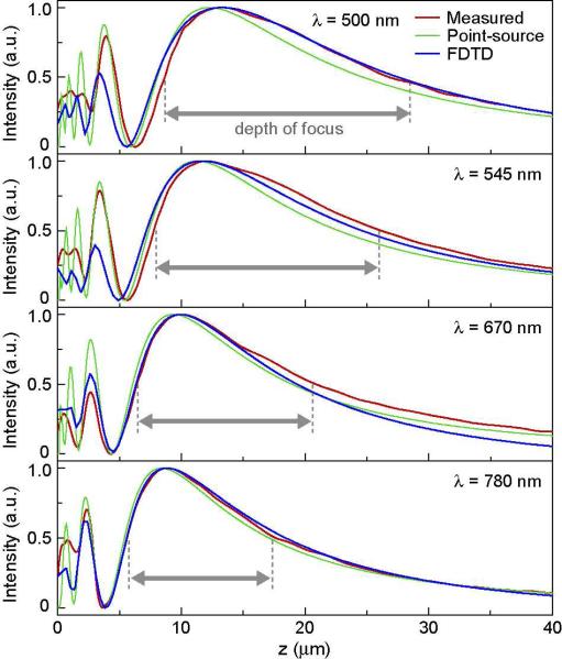
To model the focusing effects of lenses with circular nanoholes, we carried out analytical calculations by considering each nanohole as a point dipole source of light. The calculated optical field distributions agree very well with experiment (Fig. 2, red and green curves) and indicate that the focal spot is formed from the interference of in-phase electromagnetic (EM) waves emerging from the nanoholes (Fig. S2). Also, excellent agreement is seen in far-field optical patterns simulated using the finite-difference time-domain (FDTD) method (Fig. 2, red and blue curves). The simulated near-field distributions provide additional confirmation that the EM waves transmitted through every nanohole have the same phase and similar amplitude (Fig. S3). This phase-coherence is a direct result of normal incidence excitation of surface plasmons in the nanohole array: plasmon oscillations that are in-phase among nanoholes on the input surface (glass-gold interface) remain in-phase on the output surface (gold-air interface) after transmission. Hence, similar to a single aperture of the same overall size (Fig. S4), the focal length of a patch is proportional to its diameter and inversely proportional to the square root of the operating wavelength (Eq. (1)).30
Figure 2. Confocal optical measurements, point-source calculations and FDTD simulations showed excellent agreement on focal length and depth of focus for a 5-μm patch.
z-linescans of measured and simulated 3D optical field maps for the patch in Fig. 1 are shown at (A) λ = 500 nm, (B) λ = 545 nm, (C) λ = 670 nm, and (D) λ = 780 nm.
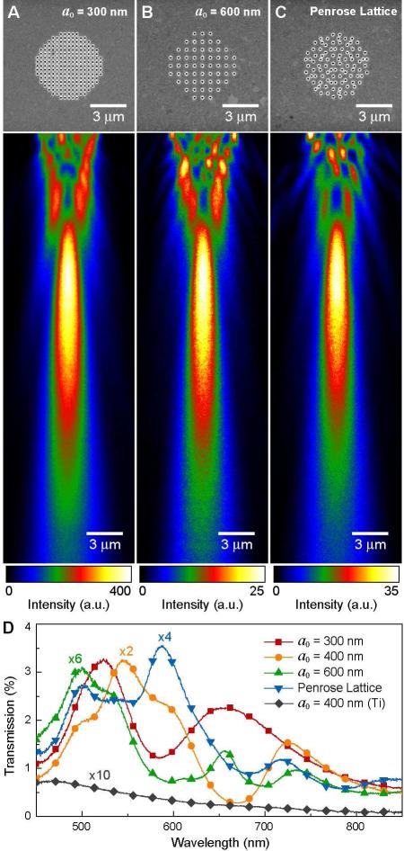
Because their focusing effects are not a consequence of phase-front engineering, 5-μm patches with periodic or aperiodic lattices had nearly identical focal spots (Fig. 3A-3C). Radial symmetry is absent, however, in the region near the patch surface of the Penrose lattice because of aperiodicity (Fig. 3C). Although the 3D transmission pattern (e.g. focal length, depth of focus, focal spot size) can be explained by a model treating the nanoholes as identical point dipoles, the optical throughput and the intensity of the focal spot depend on surface plasmon-enhanced transmission through the subwavelength apertures. Figure 3D compares the transmission spectra from the different 5-μm patches, where surface plasmon polariton (SPP) Bloch wave modes31-34 were present at different wavelengths depending on the lattice symmetry. The SPP resonances are broadened significantly compared to those supported by infinite hole arrays because of the finite-size of the patches.35 Since subwavelength circular holes do not support photonic modes,36 SPP-enhanced optical transmission is critical to observe focusing.35, 37, 38 Evidence that the transmission is mediated by surface plasmons is demonstrated in a control experiment on patches in Ti (a non-plasmonic material at optical frequencies) (Fig. S5). With geometric parameters identical to the Au patch in Fig. 1, a Ti patch showed optical throughput much lower over a broadband range (and 40 times lower at λ = 780 nm).
Figure 3. Focal spots from patches of the same size were independent of lattice symmetry.
The location and the geometry of the focal spot did not change when (A) a0 (= 400 nm in Fig. 1) was reduced to a0 = 300 nm, (B) increased to a0 = 600 nm, or (C) in an aperiodic array (Penrose lattice) at λ = 670 nm. (D) Surface plasmon resonances were tuned by changing the lattice geometry, which provides a means to control the optical throughput of the microlenses at specific wavelengths. The transmission spectrum of Ti patches exhibited much lower amplitudes than Au.
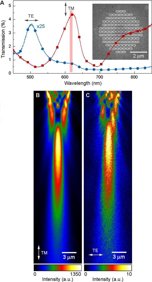
Microlenses that rely on surface plasmon-mediated optical transmission can be easily designed and fabricated with polarization sensitivity. Patches with anisotropic hole shapes (all the same size) exhibited a high polarization ratio:39 the transmission of TM-light with electric field polarized perpendicularly to the long axis of the hole was two orders of magnitude higher than the transmission of TE-light at a SPP resonance (Fig. 4A). Such a high polarization ratio can also be observed in the focusing effect. Despite similarities in the optical pattern to patches of circular nanoholes in Fig. 1, the intensity of the focal spot from TM-light was more than 100 times that of TE-light (Fig. 4B).
Figure 4. Plasmon-enhanced transmission provides means to tune the optical throughput by polarization.
Nanoholes were patterned with an aspect ratio of 7:1 (350 nm × 50 nm). (A) At the plasmon resonance, the transmission intensity of TM light (electric field along the short axis of the nanoholes) at λ = 620 nm was more than two orders of magnitude higher than that under TE light. The intensity difference was also observed in the confocal scanning optical images under (B) TM- and (C) TE-polarized illumination.
The light transmitted through the patches was also highly directional. This beaming is reminiscent of transmission from single nanoholes surrounded by periodic grooves,40, 41 although the latter effect results from interference among scattered plasmon waves at the central hole. The directional emission of light from the patches suggests that neighboring patches can be situated in close proximity without obvious interference between their light beams. We demonstrated that 5-μm patches patterned edge-to-edge and with no inter-patch spacing maintained high focusing integrity (Fig. S6). The minimal crosstalk between adjacent patches makes the plasmonic microlenses promising for high-density photodetector arrays42 and high-throughput photolithography,8 where close-packed arrays of miniaturized microlenses are desirable.
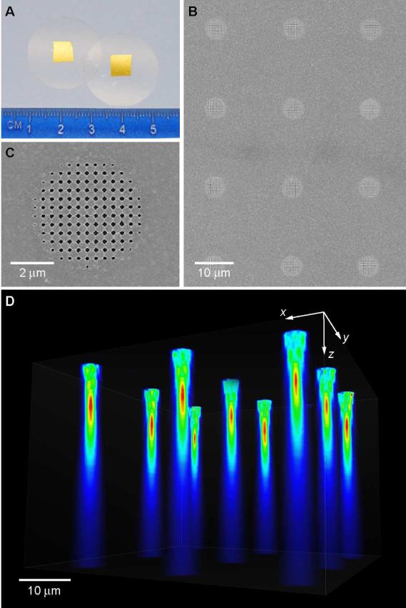
Although FIB is a powerful tool that is useful for prototyping plasmonic microlenses, highly parallel fabrication methods are needed to create large-area arrays. We used soft interference lithography (SIL) followed by PEEL35, 43 to create arrays of 5-μm Au patches of nanoholes on a 20-μm pitch (Fig. 5A-5B). One perceived disadvantage of this high throughput, hierarchical technique is that finite-sized areas often have smaller nanohole sizes around the edges of the microscale patterns (Fig. 5C). The nonuniformity in size did not dramatically affect the performance of the patch, however; each microlens in the array still exhibited highly directional beaming with independent foci. Significantly, the arrays of patches focus broadband (white) light (Fig. 5D) due to the minimal chromatic aberration. The focal points under white light illumination had the same lateral dimensions as those under single wavelengths, while the broadband focal length was approximately the average of the focal lengths at SPP wavelengths (i.e. 570 nm and 700 nm for the patch arrays, Fig. S7). The primary optical difference between FIB and SIL-PEEL generated microlenses of ostensibly the same size (diameter = 5 μm) was the slight decrease in focal length. The source amplitudes were diminished towards the outside of the patch because of the smaller holes on the perimeter, which effectively reduced the number of nanoholes (and overall patch diameter) contributing to the optical diffraction pattern. Smaller diameter patches, therefore, exhibited shorter focal lengths (Fig. S8).
Figure 5. Broadband (white) light can be focused by large-area plasmonic microlens arrays.
(A) Photograph of Au films perforated with arrays of patches on glass cover slips. (B)-(C) SEM images of the 5-μm patches patterned 20 μm apart (center-to-center) using a high-throughput soft nanolithographic method. (D) 3D optical image from a wide-field optical microscope. Identical foci from individual patches were observed under broadband illumination.
In summary, we have introduced a new type of plasmonic diffractive lens based on patches of circular nanoholes that can be patterned in arrays over wafer-sized areas. The patches focus and beam light with single-element dimensions drastically smaller than conventional diffractive microlenses. Supported by analytical calculations and numerical simulations, the focusing and beaming properties of the patches can be explained by a combination of both optical diffraction and surface plasmon effects. Moreover, patch substructure can be tailored to provide high transmission at specific wavelengths and effectively operate as a tunable band-pass filter. The broadband focusing capabilities of the patches sets them apart from other diffractive and refractive microlenses and opens applications in multi-color stereo imaging, broadband light collection, and multi-channel optical communication.
Supplementary Material
Acknowledgments
We thank Joel Henzie for carrying out preliminary experiments, George C. Schatz and Jeffrey M. McMahon for discussions, and Mark D. Huntington and Wei Zhou for help with sample processing. This work was supported by the NIH Director's Pioneer Award (DP1OD003899, TWO) and the NSF-MRSEC (DMR-0520513, LJL). This work made use of the NUANCE Center facilities, which are supported by NSF-MRSEC, NSF-NSEC, and the Keck Foundation.
Footnotes
Supporting Information is available free of charge via the Internet at http://pubs.acs.org.
References
- 1.Borrelli NF. Microoptics Technology. 2 ed. Marcel Dekker; New York: 2005. [Google Scholar]
- 2.Edwards CA, Presby HM, Dragone C. J. Lightwave Technol. 1993;11:252–257. [Google Scholar]
- 3.Ee Y-K, Arif RA, Tansu N, Kumnorkaew P, Gilchrist JF. Appl. Phys. Lett. 2009;91:221107. [Google Scholar]
- 4.Arai J, Kawai H, Okano F. Appl. Opt. 2006;45:9066–9078. doi: 10.1364/ao.45.009066. [DOI] [PubMed] [Google Scholar]
- 5.Arimoto H, Javidi B. Opt. Lett. 2001;26:157–159. doi: 10.1364/ol.26.000157. [DOI] [PubMed] [Google Scholar]
- 6.Nussbaum P, Völkel R, Herzig HP, Eisner M, Haselbeck S. Pure Appl. Opt. 1997;6:617. [Google Scholar]
- 7.Quake SR, Scherer A. Science. 2000;290:1536–1540. doi: 10.1126/science.290.5496.1536. [DOI] [PubMed] [Google Scholar]
- 8.Chao D, Patel A, Barwicz T, Smith HI, Menon R. J. Vac. Sci. Technol. B. 2005;23:2657–2661. [Google Scholar]
- 9.Kemme SA, Cruz-Cabrera AA. Fabricating Surface-Relief Diffractive Optical Elements. In: Kemme SA, editor. Microoptics and Nanooptics Fabrication. CRC Press; 2010. [Google Scholar]
- 10.Barnes WL, Dereux A, Ebbesen TW. Nature. 2003;424:824–830. doi: 10.1038/nature01937. [DOI] [PubMed] [Google Scholar]
- 11.Ozbay E. Science. 2006;13:189–193. doi: 10.1126/science.1114849. [DOI] [PubMed] [Google Scholar]
- 12.Pendry JB, Martín-Moreno L, Garcia-Vidal FJ. Science. 2004;305:847–848. doi: 10.1126/science.1098999. [DOI] [PubMed] [Google Scholar]
- 13.Ebbesen TW, Lezec HJ, Ghaemi HF, Thio T, Wolff PA. Nature. 1998;391:667–669. [Google Scholar]
- 14.García-Vidal FJ, Lezec HJ, Ebbesen TW, Martín-Moreno L. Phys. Rev. Lett. 2003;90:213901. doi: 10.1103/PhysRevLett.90.213901. [DOI] [PubMed] [Google Scholar]
- 15.Liu H, Lalanne P. Nature. 2008;452:728–731. doi: 10.1038/nature06762. [DOI] [PubMed] [Google Scholar]
- 16.Bozhevolnyi SI, Volkov VS, Devaux E, Laluet J-Y, Ebbesen TW. Nature. 2006;440:508–511. doi: 10.1038/nature04594. [DOI] [PubMed] [Google Scholar]
- 17.Lal S, Link S, Halas NJ. Nature Photon. 2007;1:641–648. [Google Scholar]
- 18.Dionne JA, Lezec HJ, Atwater HA. Nano Lett. 2006;6:1928–1932. doi: 10.1021/nl0610477. [DOI] [PubMed] [Google Scholar]
- 19.Hill MT, Oei Y-S, Smalbrugge B, Zhu Y, Vries T. d., Veldhoven P. J. v., Otten F. W. M. v., Eijkemans TJ, Turkiewicz JP, Waardt H. d., Geluk EJ, Kwon S-H, Lee Y-H, Nötzel R, Smit MK. Nature Photon. 2007;1:589–594. [Google Scholar]
- 20.Oulton RF, Sorger VJ, Zentgraf T, Ma R-M, Gladden C, Dai L, Bartal G, Zhang X. Nature. 2009;461:629–632. doi: 10.1038/nature08364. [DOI] [PubMed] [Google Scholar]
- 21.Noginov MA, Zhu G, Belgrave AM, Bakker R, Shalaev VM, Narimanov EE, Stout S, Herz E, Suteewong T, Wiesner U. Nature. 2009;460:1110–1112. doi: 10.1038/nature08318. [DOI] [PubMed] [Google Scholar]
- 22.Verslegers L, Catrysse PB, Yu Z, White JS, Barnard ES, Brongersma ML, Fan S. Nano Lett. 2008;9:235–238. doi: 10.1021/nl802830y. [DOI] [PubMed] [Google Scholar]
- 23.Liu Z, Durant S, Lee H, Pikus Y, Fang N, Xiong Y, Sun C, Zhang X. Nano Lett. 2007;7:403–408. doi: 10.1021/nl062635n. [DOI] [PubMed] [Google Scholar]
- 24.Huang FM, Kao TS, Fedotov VA, Chen Y, Zheludev NI. Nano Lett. 2008;8:2469–2472. doi: 10.1021/nl801476v. [DOI] [PubMed] [Google Scholar]
- 25.Lin L, Goh XM, McGuinness LP, Roberts A. Nano Lett. 2010;10:1936–1940. doi: 10.1021/nl1009712. [DOI] [PubMed] [Google Scholar]
- 26.Lerman GM, Yanai A, Levy U. Nano Lett. 2009;9:2139–2143. doi: 10.1021/nl900694r. [DOI] [PubMed] [Google Scholar]
- 27.Huang FM, Chen Y, Abajo F. J. G. d., Zheludev NI. J. Opt. A. 2007;9:S285. [Google Scholar]
- 28.Dennis MR, Zheludev NI, Abajo F. J. G. d. Opt. Express. 2007;15:9692–9700. doi: 10.1364/oe.15.009692. [DOI] [PubMed] [Google Scholar]
- 29.O'Shea DC, Suleski TJ, Kathman AD, Prather DW. Diffractive Optics: Design, Fabrication, and Test. TT62. SPIE Publications; 2003. [Google Scholar]
- 30.Ruffieux P, Scharf T, Herzig HP, Völkel R, Weible KJ. Opt. Express. 2006;14:4687–4694. doi: 10.1364/oe.14.004687. [DOI] [PubMed] [Google Scholar]
- 31.Barnes WL, Murray WA, Dintinger J, Devaux E, Ebbesen TW. Phys. Rev. Lett. 2004;92:107401. doi: 10.1103/PhysRevLett.92.107401. [DOI] [PubMed] [Google Scholar]
- 32.Gao H, Henzie J, Lee MH, Odom TW. Proc. Natl. Acad. Sci. U.S.A. 2008;105:20146. doi: 10.1073/pnas.0809034105. [DOI] [PMC free article] [PubMed] [Google Scholar]
- 33.Przybilla F, Genet C, Ebbesen TW. Appl. Phys. Lett. 2006;89:121115. [Google Scholar]
- 34.Bravo-Abad J, Fernández-Domínguez AI, García-Vidal FJ, Martín-Moreno L. Phys. Rev. Lett. 2007;99:203905. doi: 10.1103/PhysRevLett.99.203905. [DOI] [PubMed] [Google Scholar]
- 35.Henzie J, Lee MH, Odom TW. Nature Nanotech. 2007;2:549–554. doi: 10.1038/nnano.2007.252. [DOI] [PubMed] [Google Scholar]
- 36.Bethe HA. Phys. Rev. 1944;66:163–182. [Google Scholar]
- 37.Gao H, Henzie J, Odom TW. Nano Lett. 2006;6:2104–2107. doi: 10.1021/nl061670r. [DOI] [PubMed] [Google Scholar]
- 38.Gordon R, Brolo A. Opt. Express. 2005;13:1933–1938. doi: 10.1364/opex.13.001933. [DOI] [PubMed] [Google Scholar]
- 39.Koerkamp KJK, Enoch S, Segerink FB, Hulst N. F. v., Kuipers L. Phys. Rev. Lett. 2004;92:183901. doi: 10.1103/PhysRevLett.92.183901. [DOI] [PubMed] [Google Scholar]
- 40.Lezec HJ, Degiron A, Devaux E, Linke RA, Martin-Moreno L, Garcia-Vidal FJ, Ebbesen TW. Science. 2002;297:820–822. doi: 10.1126/science.1071895. [DOI] [PubMed] [Google Scholar]
- 41.Yu N, Fan J, Wang QJ, Pflügl C, Diehl L, Edamura T, Yamanishi M, Kan H, Capasso F. Nature Photon. 2008;2:564–570. [Google Scholar]
- 42.Caijun Ke1 XY. Jianjun Lai1 and Sihai Chen1. J. Micromech. Microeng. 2004;14:125–128. [Google Scholar]
- 43.Henzie J, Lee J, Lee MH, Hasan W, Odom TW. Ann. Rev. of Phys. Chem. 2009;60:147. doi: 10.1146/annurev.physchem.040808.090352. [DOI] [PubMed] [Google Scholar]
Associated Data
This section collects any data citations, data availability statements, or supplementary materials included in this article.


