Abstract
In this paper, we have demonstrated that europium oxide (Eu2O3) is a new type of active catalyst for single-walled carbon nanotubes (SWNTs) growth under suitable conditions. Both random SWNT networks and horizontally aligned SWNT arrays are efficiently grown on silicon wafers. The density of the SWNT arrays can be altered by the CVD conditions. This result further provides the experimental evidence that the efficient catalyst for SWNT growth is more size dependent than the catalysts themselves. Furthermore, the SWNTs from europium sesquioxides have compatibly higher quality than that from Fe/Mo catalyst. More importantly, over 80% of the nanotubes from Eu2O3 are semiconducting SWNTs (s-SWNTs), indicating the preferential growth of s-SWNTs from Eu2O3. This new finding could open a way for selective growth of s-SWNTs, which can be used as high-current nanoFETs and sensors. Moreover, the successful growth of SWNTs by Eu2O3 catalyst provides new experimental information for understanding the preferential growth of s-SWNTs from Eu2O3, which may be helpful for their controllable synthesis.
Keywords: Preferential growth, Semiconducting single-walled carbon nanotubes, Europium oxide
Introduction
Single-walled carbon nanotubes (SWNTs) have attracted a great deal of attention due to their unique structures and excellent properties [1-4] since their discovery [5]. Several approaches [6-8] have been developed for the preparation of SWNTs, among which the catalyst plays an important role in the chemical vapor deposition (CVD) process of SWNTs [9]. It is generally accepted that the nanoscaled catalyst particles act as the initiating centers and the SWNTs grow out from them via a vapor–liquid–solid (VLS) mechanism [10]. The Fe-family elements are known to be the most common catalysts, and both experimental [11] and theoretical [12,13] studies show their high catalytic activities. However, in the past 5 years, many other metals such as Ag, Pd, Au, Cu, Rh, Pb [14-19], Mg, Mn, Cr, Sn and Al [20,21], semiconductors such as Si and Ge [16], carbides such as SiC [16], Fe3C [22] and more recently even oxides including SiO2, Al2O3, TiO2 have been reported to be active for SWNT growth [23]. These materials were regarded as inactive catalysts for the growth of CNTs in the past. Therefore, these findings challenge the traditional thinking about the growth of CNTs and the role of the catalysts. Furthermore, different types of catalysts will provide more chance to understand the relationship between the catalyst and the structures of the SWNTs and thus may find out the approach for selective growth of semiconducting SWNTs (s-SWNTs) or metallic SWNTs (m-SWNTs). For SWNT-based electronics applications such as field-effect transistor (FET), pure s-SWNT can be used as high-current nanoFETs and sensors. A lot of efforts have been focused on generating pure s- or m-SWNTs including selective growth of s- or m-SWNTs [24-26], electrical breakdown of m-SWNTs based on FET devices [27], electrochemical and solution-phase chemical separation [28], selective chemical reaction [29-31] and more recently irradiation [32,33].
In this contribution, we first report that random and superlong well-oriented SWNT arrays can be generated by CH4-CVD or EtOH-CVD from rare earth metal oxide Eu2O3. The Raman spectroscopy with the combination of electrochemical deposition of Ag has been applied to evaluate the structure of the as-grown SWNTs. This new type catalyst provides not only an alternative catalyst for the growth of SWNTs but also a possible high percentage of superlong s-SWNT arrays for various SWNT-based nanodevice fabrications and applications.
Experimental Methods
Growth of SWNTs from Eu2O3 Nanoparticles on SiO2/Si Wafers
Si wafer with 500-nm layer of SiO2 was first cleaned by H2SO4/H2O2 solution (the volume ratio of H2SO4 to H2O2 is 7:3) followed by washing with deionized water and acetone under sonication before use. Eu(NO3)3 was purchased from Aldrich with purity higher than 99.99%. The catalyst precursor was loaded onto the substrate by dipping the wafer into 1 mM ethanol solution of Eu(NO3)3. CH4-CVD or EtOH-CVD was carried out. When gradual heating in H2 (800 sccm) until 900°C, CH4 (200 sccm)/H2 (300 sccm) or ethanol vapor delivered by bubbling H2 (200 sccm) into ethanol which has 1–3% water at 25–40°C with argon (200 sccm) was introduced into the 1-in.-diameter quartz tube. The growth of the nanotubes lasted for 10 min.
Deposition of Ag on SWNT Arrays
The electrodeposition was carried out using a three-electrode arrangement [34], a saturated calomel electrode as the reference electrode, Pt gauze counter electrode, and working electrode which is the long-oriented SWNT arrays connected by a conducting silver adhesive or Au layer by sputtering coating. The samples were dipped into the silver deposition solution containing 0.1 mM AgNO3 (99+%, Aldrich Chemicals) with 20 mM KNO3 (analytical grade, Beijing reagents) as the supporting electrolyte. Electrodeposition was performed at −0.6 V for 10 s.
Characterization
SEM images were taken from FEI NanoSEM at 1 kv, spot 4 or 10 kv, spot 3. TEM images of SWNTs were taken from Si3N4 window where the nanotube grew in situ using a Philips CM200 TEM at 200 kV. AFM images were recorded at NanoScope IIIa atomic force microscope from Veeco, Inc. in tapping mode at room temperature. Raman spectra of SWNTs on either silicon wafers or quartz plates were collected from JY-T64000 Raman spectroscopy under ambient conditions by using excitation laser lines of 514.5 nm (2.41 eV) or 632.8 nm (1.96 eV) from an air-cooled Ar+ laser. The beam size is 2 µm. The laser power was carefully controlled to avoid any heating effects.
Result and Discussion
Growth of SWNTs on SiO2/Si Wafers
In order to avoid possible metal contamination in the CH4-CVD system and possible impurity of chemicals, a new quartz reactor was used for each experiment. A clean SiO2/Si wafer was put in front of the substrate as a reference to observe if any nanotubes formed without the catalyst. From SEM observation, many carbon nanotubes could be found on the substrate with Eu(NO3)3, but no nanotube was observed on the clean wafer. Interestingly, as-grown SWNTs were often tangled with each other and formed round-like shapes as shown in Fig. 1a. Such high-density SWNT films show attractive applications in SWNT-based thin-film transistors [35]. Raman spectroscopy provides a powerful tool to characterize the diameter and quality of SWNTs. Figure 1b, 1c shows the typical Raman spectra of radial breathing mode (RBM) peaks and G-band of two different positions of Fig. 1a, respectively. The peaks of the RBM at 221.8, 223.1, 229.1, 230.8 and 234.7 cm−1 correspond to SWNTs with the diameters of 1.12, 1.11, 1.08, 1.07 and 1.05 nm, respectively, according to the equation of d = 248 cm−1/ω [36]. It is known that the D-band is related to vacancies, impurities, or other symmetry-breaking defects in SWNTs. Herein, the quite weak D-band shows that the as-prepared SWNTs by this method are of high quality.
Figure 1.
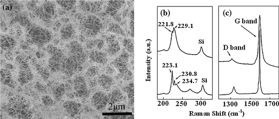
a SEM images of the as-grown SWNTs on substrates by CH4-CVD, Raman spectra of SWNTs from two different positions of the same sample in (a). Raman spectra b and c are RBM and G-band, respectively
To confirm that it was Eu2O3 nanoparticles that acted as the catalyst during the CVD process, we undertook the energy-disperse X-ray spectrum (EDX) measurement on the carbon nanotubes with particles on Cu grid. The results indicate the catalyst particle contain large amount of oxygen atoms as shown in Fig. 2, suggesting that it exhibited an oxide state; in addition, it was needed to point out that Fe, Co, Ni and any other metal elements were not found in the sample, indicating that it was europium oxide that acted as catalyst in the growth process. Before the XRD was performed, we put the solid state of Eu(NO3)3 into porcelain boat, then it was heated at 900°C and lasted for 10 min under H2 atmosphere. Figure 3 is the XRD pattern of the samples. In the XRD pattern, the peaks at different angle are indexed to diffraction lines from the (222), (400), (440) and (622) planes of Eu2O3 (PDF, 34-0392). Interestingly, the diffraction peaks of Eu2O3 are so strong at plane (222), (400). It may caused by the well-crystallized large catalyst particles existing in the samples. The above-mentioned results display that, unlike the traditional metallic or carbide catalysts, it is the Eu2O3 that acted as a catalyst during the growth of nanotubes. No metal Eu was formed on the substrate under the hydrogen atmosphere according to Fig. 3. It was possibly caused by the low standard electrode potential of Eu2O3 (Eu3+→Eu, −2.407 V), which showed that hydrogen could not reduce Eu2O3 to metal Eu.
Figure 2.
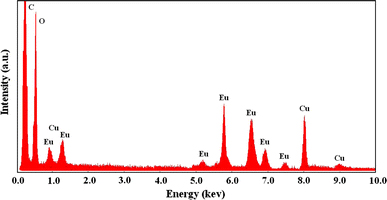
The EDX analysis of nanoparticles contained in a SWNT tip on Cu toil
Figure 3.
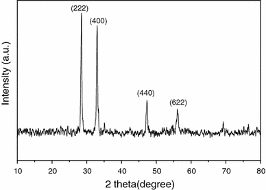
XRD pattern of the decomposition product of catalyst precursor
In our recent article [23], we have demonstrated that nano-sized oxides including SiO2, TiO2 and Al2O3 are effective for SWNT growth and proposed that any materials with suitable size may be active for nanotube growth. After the substrate with Eu(NO3)3 was treated at 900°C for 5 min, AFM observation showed that Eu2O3 nanoparticles with different sizes were formed due to the decomposition of Eu(NO3)3 (Fig. 4a). AFM was also employed to investigate the diameter of SWNTs, and AFM image of the as-grown nanotubes is shown in Fig. 4b. The height measured on random nanotubes (total of 102 nanotubes were measured) indicated that the SWNTs had an average diameter of about 1.27 nm (Fig. 4c). Small amounts of the large-diameter nanotubes (>2 nm) may be due to small bundles of SWNTs, double-walled CNTs or contamination such as amorphous carbon surrounding the nanotube surface. In addition, the mean diameter from TEM measurements of 95 SWNTs is 1.264 nm, which is slightly smaller than that of AFM.
Figure 4.
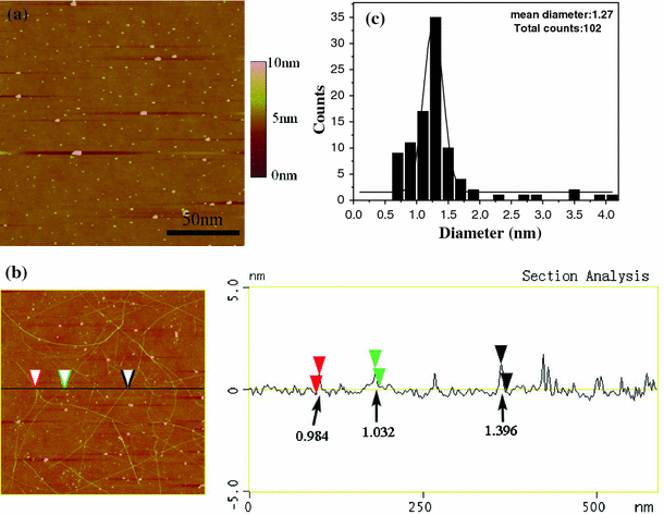
a AFM image of Eu2O3 particles on substrate after thermal treatment at 900°C; b AFM image and height profile of the nanotubes growing from Eu2O3; c diameter distribution of the nanotubes based on AFM height measurement
Figure 5a shows the typical SEM image of the as-prepared SWNT arrays via EtOH-CVD at 900°C, employing the fast-heating method and the catalyst area as indicated by white arrow. Large area and well-aligned SWNT arrays are obtained. The SEM-magnified image of upright inset indicates that the density is about 2 SWNTs/10 µm and the nanotube is very straight. SEM image is shown in Fig. 5b using the ordinary CVD method, and the inset is TEM image. TEM observation on Si3N4 window further verifies that the as-grown nanotubes are SWNTs. It can be seen from the SEM observation that the horizontally aligned SWNT arrays are uniform over a large area, and the density of the parallel SWNTs is about 3–4 SWNTs/20 µm. Though this density is lower than those of aligned SWNT arrays grown on quartz [37] and sapphire [38], it is still very high among reports of horizontally aligned SWNT arrays on silicon wafers [39]. The length of the wafer is about 1.5 cm. Most of the nanotubes can grow from one side to another side of the substrate, indicating the length of the SWNT arrays in centimeter scale. Such large-area uniform SWNT arrays show attractive applications in various SWNT-based nanodevices.
Figure 5.
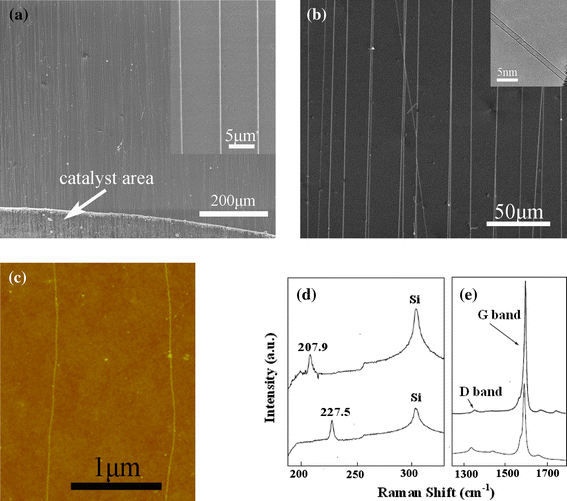
a, b SEM image of well-oriented SWNT arrays on SiO2/Si wafer by EtOH-CVD at 900°C, a using the fast-heating method, and the inset is its part magnified image, b using the ordinary method, and the right inset is TEM image of individual nanotube, c AFM image of the as-grown SWNTs, Raman spectra d and e are RBM and G-band, respectively, of two different SWNTs in sample (b)
We carry out AFM and Raman measurements on two SWNTs. Figure 5c shows the AFM image of two SWNTs in the same sample with that in Fig. 5b. The corresponding Raman spectra (Fig. 5d, 5e) gave the RBM bands at 207.9 and 227.5 cm−1. We can calculate the corresponding diameters of the two SWNTs, which are 1.19 and 1.09 nm according to the equation of d = 248 cm−1/ω [36], which is within the range obtained from our AFM and TEM observations. The typical Raman spectra with 632.8-nm lasers are shown in Fig. 5e. It can be seen that the strong G-band peaks at about 1,590 cm−1 correspond to graphitic structure and the weak D-band peaks indicate a good quality of SWNTs.
The activity of the Eu2O3 for growing SWNTs further supports our thinking. Although Eu2O3 had little solubility of carbon and did not decompose organic molecules catalytically at room temperature, we believe that, at high temperature, the high fluctuation of the nano-sized liquid-like structure of the molten Eu2O3 activated organic molecules and initiated the nucleation and growth of nanotubes. In fact, rare earth oxides have catalytic function for many reactions such as oxidative couple, H/D exchange and NO reduction with CH4, decomposition of alcohols, and chemical adsorption of NH3 and CO2[40] that involves the activating dissociation of C–H, C–O, H–H and N–H bonds. It is well known that defects in a solid could dramatically influence its chemical reactivity. High-temperature treatment on these sesquioxides causes more oxygen vacancies and promotes their catalytic activity [13]. Moreover, metal atoms in bulk rare earth oxides have high mobility and start to migrate at Tammann temperature (half of melting point, ~1,200°C), and oxygen substructure is mobile in even much lower temperature [41]. The melting point of Eu2O3 is 2,291°C; however, it is expected that the melting point of nano-sized oxides (<2 nm) is lower than the growth temperature (900°C). Thus, high activity for Eu2O3 nanoparticles to catalytically grow SWNTs can be understandable.
As reported in our previous paper [34], Ag can be electrochemically deposited onto the both m-and s-SWNTs with no defects along the long-oriented SWNTs. To further investigate the quality of the SWNTs, we carried out typical electrochemical experiment in the horizontally long SWNT arrays. Figure 6a shows schematic representation of the three main processes in our experiment, from coating the catalyst precursor to horizontally aligned SWNT arrays grown to the electrodeposition of silver on SWNT arrays. Figure 6b is the SEM image showing the well-aligned SWNTs after electrodeposition of Ag for 10 s in 0.1 mM AgNO3 solution at −0.6 V. It is interesting that the small amount of nanotubes do not have Ag deposition (Tube1, Tube3 and Tube2 are with and without Ag deposition, respectively, indicated by the black arrow.). After careful checking with these long nanotubes, 321 out of 350 nanotubes are found to be deposited with Ag (91.7%) and only 8.3% SWNTs are without Ag deposition. However, for Fe/Mo nanoparticles catalyst system, the percentage of the nanotubes with Ag deposition is ~68% [34], This result indicates that the SWNTs grew from Eu2O3 have much better structural uniformity with less defects than that from Fe/Mo catalyst.
Figure 6.
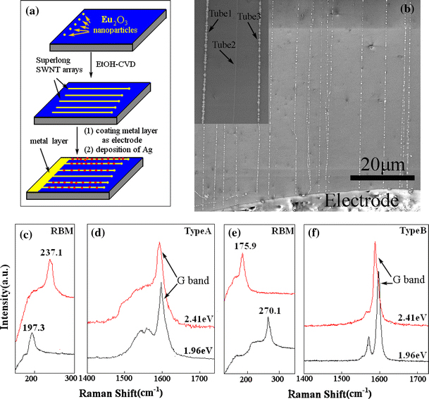
a Schematic representation of the process from coating the catalyst precursor to the electrodeposition of silver on SWNT arrays. b SEM image of the superlong well-oriented SWNT arrays after Ag deposition. Inset is the amplified image showing the nanotubes with and without Ag deposition. Raman spectra from isolated individual SWNTs using two different excitation laser lines of 2.41 and 1.96 eV: c RBM and d G-band features of type A, e RBM and f G-band features of type B
Resonant Raman spectroscopy has been proven to be a powerful tool for characterizing and revealing the detailed structure and the electronic and phonon properties of SWNTs. The RBM and G-band features of Raman spectra can be used to assign and distinguish the s- and m-SWNTs, especially when multiple excitation lasers are used. G-mode of m-SWNT has broadened line shape fitting with Breit–Wigner–Fano (BWF) line and s-SWNT has Lorentzian line shape. Applying Raman spectroscopy with the assistance of the Ag deposition, we are able to identify the structure of an individual nanotube. We note that the G-band of the SWNT arrays can be easier to be collected using 2.41 eV laser at relative high power of the laser. We checked 101 long nanotubes with Ag deposition and found that except 4 nanotubes that are undetectable (out of Raman resonance window), 85 out of 101 are s-SWNTs that has typical Raman spectrum as shown in Fig. 6f and only 12 is m-SWNTs (Fig. 6d). In order to avoid possible bundle of the long SWNTs, we checked the nanotubes carefully one by one via SEM to make sure that the nanotube is individual before Raman identification. We calculate that over 80% of the nanotubes are s-SWNTs, indicating the preferential growth of s-SWNTs by using Eu2O3 as catalyst.
Since the Raman resonance of the SWNTs depends on both excitation frequency and the diameter of the SWNT, it is necessary to use another laser line to identify the structures of the SWNTs. We further check the SWNTs by using Elaser 632.8 nm (Elaser = 1.96 eV) to collect the G-band from 40 long tubes, among which 37 nanotubes have Ag particles and find 33 s-SWNTs (82.5%) and 3 m-SWNTs (7.5%). The typical Raman spectra are shown in Fig. 6d, 6f. The percentage of the s-SWNTs measured from 1.96 eV excitation laser line is similar to that from 2.41 eV.
To further confirm a high percentage of semiconducting nanotubes in these SWNT arrays, we simultaneously examined the corresponding RBM peaks as shown in Fig. 6c, 6e. According to the equation of d = 248 cm−1/ω, we can obtain metallic nanotubes of 1.05 and 1.26 nm diameter and semiconducting nanotubes of 1.41 and 0.92 nm diameter using 2.41 and 1.96 eV, respectively, which is within the range of Kataura plot [42,43]. We can see that the RBM results agree with the G-band features of Raman spectra.
The high percentage of the s-SWNTs in the long-oriented SWNT arrays from Eu2O3 is believed to relate to the defects caused during prolonged growth period and their tip-growth mechanism. A high percentage of s-SWNTs both vertically and horizontally aligned SWNT arrays on substrate have been reported more recently [29,44]. The horizontally aligned SWNT arrays can grow on ST-cut single-crystal quartz; the enrichment of s-SWNT is believed to be due to the induced growth by the substrate lattice and the optimized growth condition. The reason for the growth of vertically aligned SWNT arrays with s-SWNT still remains unclear. Further, more experiments need to be carried out for better understanding of the mechanism of the preferential growth of semiconducting structure in long SWNTs and for analysing whether other rare earth oxides have the same behavior as Eu2O3.
Conclusion
In summary, we have demonstrated that Eu2O3 is a new kind of active catalyst for SWNT growth. This result further provides the experimental evidence that the effective catalyst for SWNT growth is more size dependent than catalysts. Furthermore, the SWNTs from Eu2O3 have compatibly higher quality than that from Fe/Mo catalyst. More importantly, over 80% of the nanotubes from Eu2O3 are s-SWNTs, indicating the preferential growth of s-SWNTs from Eu2O3. This new finding could open a way to selectively growth of s-SWNT for nanoFETs and sensors in nanoelectronics devices. Further study is under way.
Acknowledgments
The work was supported in part by grants from NSFC(04640012), and the Research Program of Jiangxi Province Department of Education (No. GJJ10093) is gratefully acknowledged.
Open Access
This article is distributed under the terms of the Creative Commons Attribution Noncommercial License which permits any noncommercial use, distribution, and reproduction in any medium, provided the original author(s) and source are credited.
References
- Tans S, Verschueren A, Dekker C. Nature. 1997. p. 474. COI number [1:CAS:528:DyaK2sXisVSqt70%3D]; Bibcode number [1997Natur.386..474T] [DOI]
- Zhou C, Kong J, Dai H. Appl. 2000. p. 1597. COI number [1:CAS:528:DC%2BD3cXhsl2jsb0%3D]; Bibcode number [2000ApPhL..76.1597Z] [DOI]
- Yaish Y, Park JY, Rosenblatt S, Sazonova V, Brink M. Phys. 2004. p. 046401. COI number [1:STN:280:DC%2BD2c7gs1KhsQ%3D%3D]; Bibcode number [2004PhRvL..92d6401Y] [DOI] [PubMed]
- Kong J, Franklin N, Zhou C, Pan S, Cho K, Dai H. Science. 2000. p. 622. COI number [1:CAS:528:DC%2BD3cXovVWgtA%3D%3D]; Bibcode number [2000Sci...287..622K] [DOI] [PubMed]
- Iijima S, Ichihashi T. Nature. 1993. p. 603. COI number [1:CAS:528:DyaK3sXltVOrs7o%3D]; Bibcode number [1993Natur.363..603I] [DOI]
- Bethune DS, Kiang CH, de Vries MS, Gorman G, Savoy R, Vasquez J, Beyers R. Nature. 1999. p. 605. Bibcode number [1993Natur.363..605B] [DOI]
- Guo T, Nikolaev P, Thess A, Colbert DT, Smalley RE. Chem. 1995. p. 49. COI number [1:CAS:528:DyaK2MXnvFWisLg%3D] [DOI]
- Dai H, Rinzler AG, Nikolaev P, Thess A, Colbert DT, Smalley RE. Chem. 1996. p. 471. COI number [1:CAS:528:DyaK28Xls1yisLw%3D]; Bibcode number [1996CPL...260..471D] [DOI] [PubMed]
- Nasibulin AG, Moisala A, Brown DP, Kauppinen EI. Carbon. 2003. p. 2711. COI number [1:CAS:528:DC%2BD3sXot1GmtrY%3D] [DOI]
- Saito Y. Carbon. 1995. p. 979. COI number [1:CAS:528:DyaK2MXntFSgs74%3D]; Bibcode number [1995sfhl.book.....S] [DOI]
- Lu J, Yi SS, Kopley T, Qian C, Liu J, Gulari E. J. Phys. Chem. B. 2006. p. 6655. COI number [1:CAS:528:DC%2BD28XitVynsr0%3D] [DOI] [PubMed]
- Deng WQ, Xu X, Goddard WA. Nano Lett. 2004. p. 2331. COI number [1:CAS:528:DC%2BD2cXpsV2nt7s%3D]; Bibcode number [2004NanoL...4.2331D] [DOI]
- Liang LH, Liu F, Shi DX, Liu WM, Xie XC, Gao HJ. Phys. 2005. p. 35453. Bibcode number [2005PhRvB..72c5453L] [DOI]
- Takagi D, Homma Y, Hibino H, Suzuki S, Kobayashi Y. Nano Lett. 2006. p. 2642. COI number [1:CAS:528:DC%2BD28Xht1anurnL]; Bibcode number [2006NanoL...6.2642T] [DOI] [PubMed]
- Bhaviripudi S, Mile E, Steiner SA, Kong J. J. 2007. p. 1516. COI number [1:CAS:528:DC%2BD2sXmsVymsg%3D%3D] [DOI] [PubMed]
- Takagi D, Kobayashi Y, Hibino H, Suzuki S, Homma Y. Nano Lett. 2008. p. 832. COI number [1:CAS:528:DC%2BD1cXhs1emtr8%3D]; Bibcode number [2008NanoL...8..832T] [DOI] [PubMed]
- Zhou W, Han Z, Wang J, Zhang Y, Jin Z, Sun X. Nano Lett. 2006. p. 2987. COI number [1:CAS:528:DC%2BD28XhtFynur%2FE]; Bibcode number [2006NanoL...6.2987Z] [DOI] [PubMed]
- Ritschel M, Lenonhardt A, Elefant D, Oswald S, Büchner B. J. 2007. p. 8414. COI number [1:CAS:528:DC%2BD2sXlvVWjtL8%3D] [DOI]
- Zhang Y, Zhou W, Ding L, Zhang Z, Liang X, Li Y. Chem. 2008. p. 7521. COI number [1:CAS:528:DC%2BD1cXhsVGnsLrJ] [DOI]
- Liu B, Ren W, Gao L, Li S, Liu Q, Cheng HM. J. 2008. p. 19231. COI number [1:CAS:528:DC%2BD1cXhtlGrs77F] [DOI]
- Yuan D, Ding L, Chu H, Feng Y, McNicholas TP, Liu J. Nano Lett. 2008. p. 2576. COI number [1:CAS:528:DC%2BD1cXnvF2gsb4%3D]; Bibcode number [2008NanoL...8.2576Y] [DOI] [PubMed]
- Yoshida H, Takeda S, Uchiyama T, Kohno H, Homma Y. Nano Lett. 2008. p. 2082. COI number [1:CAS:528:DC%2BD1cXmtlGjsrY%3D]; Bibcode number [2008NanoL...8.2082Y] [DOI] [PubMed]
- Huang S, Cai Q, Chen J, Qian Y, Zhang L. J. 2009. p. 2094. COI number [1:CAS:528:DC%2BD1MXhtVaqsLk%3D] [DOI] [PubMed]
- Li Y, Mann D, Rolandi M, Kim W, Ural A, Hung S, Dai H. Nano Lett. 2004. p. 317. COI number [1:CAS:528:DC%2BD2cXltFGqsw%3D%3D]; Bibcode number [2004NanoL...4..317L] [DOI]
- Li Y, Peng S, Mann D, Cao J, Tu R, Cho KJ, Dai H. Phys. 2005. p. 6968. COI number [1:CAS:528:DC%2BD2MXisFWrurc%3D] [DOI] [PubMed]
- Li X, Tu X, Zaric S, Welsher K, Seo WS, Dai H. J. 2007. p. 15770. COI number [1:CAS:528:DC%2BD2sXhtlyqsL7N] [DOI] [PubMed]
- Collins P, Arnold M, Avouris P. Science. 2001. p. 706. COI number [1:CAS:528:DC%2BD3MXjt1els7k%3D]; Bibcode number [2001Sci...292..706C] [DOI] [PubMed]
- Zheng M, Jagota A, Strano MS, Santos AP, Barone P, Chou SG, Diner BA, Dresselhaus MS, Walls DJ. Science. 2003. p. 1545. COI number [1:CAS:528:DC%2BD3sXpt1Sms7c%3D]; Bibcode number [2003Sci...302.1545Z] [DOI] [PubMed]
- An L, Fu Q, Lu CG, Liu J, Am J. Chem. 2004. p. 10520. [DOI] [PubMed]
- Kanungo M, Lu H, Malliaras GG, Blanchet GB. Science. 2009. p. 234. COI number [1:CAS:528:DC%2BD1MXhvFemug%3D%3D] [DOI] [PubMed]
- Zhang G, Qi P, Wang X, Lu Y, Li X, Tu R, Bangsaruntip S, Mann D, Li Z, Dai H. Science. 2006. p. 974. COI number [1:CAS:528:DC%2BD28XhtFyqtLnO]; Bibcode number [2006Sci...314..974Z] [DOI] [PubMed]
- Zhang Y, Zhang Y, Xian X, Zhang J, Liu Z. J. Phys. Chem. C. 2008. p. 3849. COI number [1:CAS:528:DC%2BD1cXitVyitrw%3D] [DOI]
- Qian Y, Huang S, Gao F, Cai Q, Zhang L. J. Phys. Chem. C. 2009. p. 6983. COI number [1:CAS:528:DC%2BD1MXjvFaltbc%3D] [DOI]
- Huang S, Qian Y, Cheng J, Cai Q, Wang L, Wang S, Hu W. J. 2008. p. 11860. COI number [1:CAS:528:DC%2BD1cXpvVyjtbo%3D] [DOI] [PubMed]
- Kocabas C, Shim M, Rogers JA. J. 2006. p. 4540. COI number [1:CAS:528:DC%2BD28Xis1Khsr8%3D] [DOI] [PubMed]
- Jorio A, Saito R, Hafner JH, Lieber CM. Phys. 2001. p. 1118. COI number [1:CAS:528:DC%2BD3MXosFarug%3D%3D]; Bibcode number [2001PhRvL..86.1118J] [DOI] [PubMed]
- Kocabas C, Hur SH, Gaur A, Meitl MA, Shim M, Rogers JA. Small. 2005. p. 1110. COI number [1:CAS:528:DC%2BD2MXhtFGit7jO] [DOI] [PubMed]
- Han S, Liu X, Zhou C. J. 2005. p. 5294. COI number [1:CAS:528:DC%2BD2MXisFajtro%3D] [DOI] [PubMed]
- Huang LM, Cui XD, White B, O’Brien SP. J. Phys. Chem. B. 2004. p. 16451. COI number [1:CAS:528:DC%2BD2cXnvFSis7o%3D] [DOI]
- Adachi G, Imanaka N, Kang ZC. Binary Rare Earth Oxides. Kluwer, Dordrecht; 2004. [Google Scholar]
- Haire GR, Eyring L. Handbook on the Physics and chemistry of Rare Earth. Vol. 18. North-Holland, Amsterdam; 1994. p. 413. [Google Scholar]
- Lu W, Xiong Y, Hassanien A, Zhao W, Zheng M, Chen L. Nano Lett. 2009. p. 1668. COI number [1:CAS:528:DC%2BD1MXivFSgu78%3D]; Bibcode number [2009NanoL...9.1668L] [DOI] [PubMed]
- Kataura H, Kumazawa Y, Maniwa Y, Umezu I, Suzuki S, Ohtsuka Y, Achiba Y. Synth. 1999. p. 2555. COI number [1:CAS:528:DyaK1MXksFOnurY%3D] [DOI]
- Qu L, Du F, Dai L. Nano Lett. 2008. p. 2682. COI number [1:CAS:528:DC%2BD1cXptVOmurY%3D]; Bibcode number [2008NanoL...8.2682Q] [DOI] [PubMed]


