Abstract
Advances in the field of Micro Electro Mechanical Systems (MEMS) and their uses now offer unique opportunities in the design of ultrasensitive analytical tools. The analytical community continues to search for cost-effective, reliable, and even portable analytical techniques that can give reliable and fast response results for a variety of chemicals and biomolecules. Microcantilevers (MCLs) have emerged as a unique platform for label-free biosensor or bioassay. Several electronic designs, including piezoresistive, piezoelectric, and capacitive approaches, have been applied to measure the bending or frequency change of the MCLs upon exposure to chemicals. This review summarizes mechanical, fabrication, and electronics approaches to increase the sensitivity of microcantilever (MCL) sensors.
1. Introduction
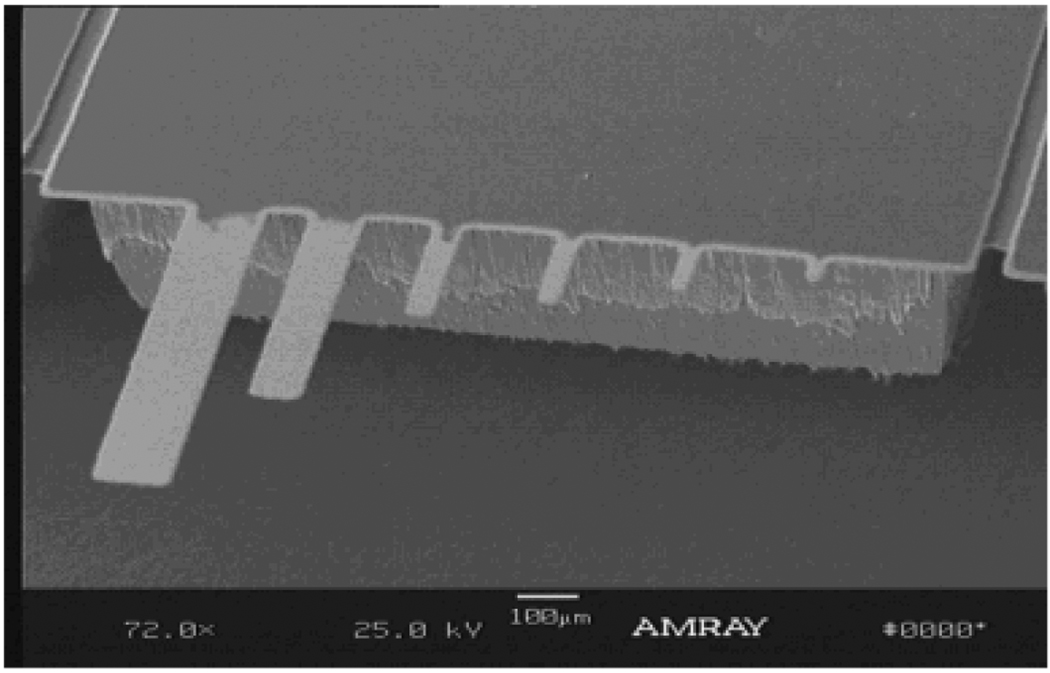
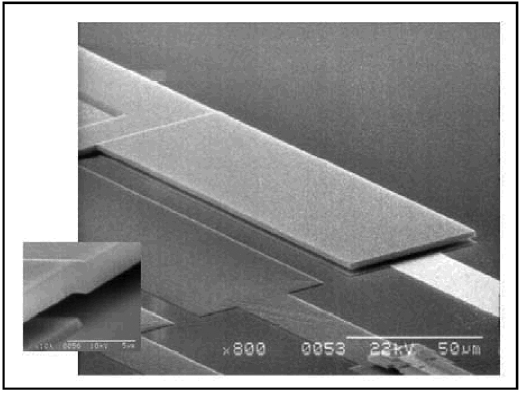
Micro Electro Mechanical Systems (MEMS) have shown tremendous growth recently. MEMS devices now offer unique opportunities in the design of ultrasensitive analytical methods. In 1994, it was realized that microcantilevers (MCLs) can be made extremely sensitive to chemical and physical changes. To date, physical sensing has been demonstrated by detecting thermal energy, strain, magnetic field, electric charge, viscosity, density, and infrared radiation. Extremely sensitive chemical vapor sensors based on MCLs have been demonstrated using selective coatings on the cantilevers. MCLs are a sort of transducers which convert physical quantity like force, strain, stress, etc. into measurable quantity such as voltage or current. MCLs are typically made in the form of rectangular or V shaped planks. An Electron micrograph of a microcantilever (MCL) array is shown in Figure 1.
Figure 1.
Electron micrographs of a MCL array.
MCLs act as a sensing platform when they are coated with a molecular recognition thin film. Absorption or adsorption of corresponding chemicals in or on the coated film results in the frequency change or bending of the MCL.
Resonant frequency
The resonant frequency, f, of an oscillating MCL can be expressed as
| (1) |
Where K is the spring constant of the lever and m* is the effective mass of the MCL. The effective mass can be related to the mass of the beam, mb, through the relation: m*=nmb, where n is a geometric parameter. It is clear that the resonant frequency can change due to changes in mass and spring constant. Resonance frequency of a MCL (dynamic mode) can be used to detect chemical species in air. However, the oscillation of the cantilever is significantly dampened in an aqueous solution, which reduces the quality factor and subsequent detection sensitivity of MCLs in aqueous solutions. It should be noted that recent results showed that the second resonance frequency of MCLs remains sharp in aqueous solutions [4] and can be used for detecting biomolecules.
MCL bending
One of the unique characteristics of MCL is that the device can be made to undergo bending due to molecular adsorption by confining the adsorption to one side of the cantilever. This bending is due to the adsorption-induced differential stress or film volume change on the cantilever (static mode).
For the surface stress induced MCL bending, from molecular point of view, the binding results in electrostatic repulsion or attraction, intermolecular interactions, or a combination of these that alter the surface stresses on the cantilever. Using Stoney’s formula [7], the bending deflection of the cantilever due to adsorption can be written as:
| (2) |
where ΔZ is the observed deflection at the end of the cantilever, ν and E are Poisson′s ratio (0.2152) and Young’s modulus (70 GPa for SiO2, 156 GPa for silicon, 300 GPa for Si3N4) for the substrate, respectively, T is the thickness of the cantilever, L is the length of the MCL, and δs is the differential stress on the MCL.
Both frequency and bending approaches have been demonstrated to detect chemicals with sensitivity as high as parts-per-trillion, and each approach has its own advantages and disadvantages which can be used for specific applications. For instance, resonance frequency of MCLs has been used to detect very low level pathogens [4, 5]; also the bending approach showed special selectivity towards some chemicals because of its unique mechanism [6]. MCL sensors hold a position as a cost-effective, sensitive sensor platform for environmental, biomedical, homeland security, and industrial applications. Compared to existing technologies for pathogen detection, the MCL sensor technology has three key advantages:
Low Cost – Electronics for operation and control are relatively simple and inexpensive.
Low-power Consumption– For static mode, since the cantilever’s bending signal is driven by molecular recognition, the only power needed is for detection and display, allowing use of light-weight battery power or photovoltaic cells.
Small Size – The entire sensor could fit in an area with its sides less than a few millimeters.
The device can be readily integrated into a robot system without much increase of weight in order to protect the operator and to guarantee uniform detection strategies.
Other than those, MCL arrays could be used to simultaneously detect and identify various chemicals on a single chip; the analysis time is relatively shorter because the assay does not require extensive sample preparation or signal amplification; it could be used for in-situ detection.
By monitoring changes in bending response or frequency change of a cantilever, mass change and surface stress changes induced by adsorption or molecular recognition can be recorded precisely and accurately. Optical, piezoresistive, piezoelectric, and capacitive methods have been used for the detection of cantilever’s deflection (Figure 2).
Figure 2.
Illustration of four methods for detecting cantilever motion with sub-nanometer precision –(Left) Laser-beam deflection method; (middle) Piezoresistive and piezoelectric method; and (Right) Capacitive method.
Each sensing mechanism has its own advantages and drawbacks. Optical method is sensitive and can measure deflection as small as 1 nm. However, the optical system is complicated and not user friendly compared to the other methods. The sensing systems based on piezoresistive, piezoelectric, and capacitive methods are much simpler and hold the potential for implantable biosensing applications. These methods do not require complex adjustment and alignment systems as needed in optical readout scheme [7–9], and they could readily be integrated with electrical circuit [10].
However, the sensitivity of these methods is generally lower than that of the optical method. Research is underway to either improve these approaches or develop new approaches for cantilever based sensing. This review summarizes recent developments in improving the sensitivity of MCL sensors based on the piezoresistive, piezoelectric, and capacitive approaches.
2. Piezoresistive Readout Scheme
The piezoresistive phenomenon is the change in resistivity of a material when subjected to stress. The piezoresistivity of a material depends on its type; the change in its geometry upon application of stress over it. Piezoresistive approach is one of the most widely applied techniques for measuring stress applied on a MCL. The advantage of this technique is that the electrical output can be readily measured and MCL can be integrated on integrated circuit (IC) [1].
In a piezoresistive MCL the relationship between the stress and the change in resistance is shown as the following equation:
| (3) |
Where, ‘R’ is initial piezoresistance, ‘ΔR’ is change in resistance; πl, πt are longitudinal and transverse piezoresistive coefficients, respectively; σl, σt are lateral and transverse stress, respectively.
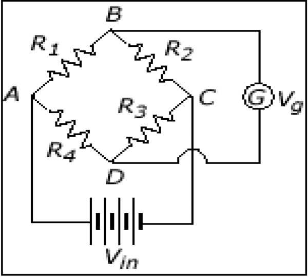
The change in the resistivity is typically measured by using a Wheatstone bridge as shown in Figure 3. A Wheatstone bridge is made up of four piezoresistors: R1, R2, R3, and R4. One of these resistors is replaced by MCL. The differential voltage (Vg) from the Wheatstone bridge is proportional to the change in the resistivity of the MCL [1].
Figure 3.
A Wheatstone bridge scheme
The output voltage from the Wheatstone bridge is given as in Equation 1.
| (4) |
Where Vin is applied input voltage. So the output voltage is directly related to the change in the resistance ΔR with respect to the initial resistance R.
The first piezoresistive MCL showed the resistivity change (ΔR/R) of 1.2×10⁻⁷ when subjected to 1 Å deflection [27]. Since then, a variety of strategies have been applied to increase the sensitivity. It should be noted that this MCL was not originally designed for sensors, but for atomic force microscopy.
2.1 Geometry optimization
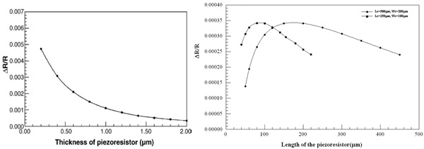
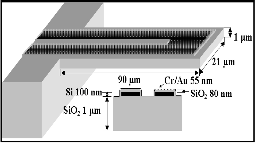
The dimensions of the MCL and the piezoresistor play a critical role in the sensitivity of MCL sensors. By using Finite Element Method (FEM) analysis, Chivukula et al. have shown that optimizing the device dimensions is useful to a greater extent in increasing the sensitivity of the device [6]. FEM analysis was done to investigate the optimized device dimensions by varying the MCL and piezoresistor geometries and the doping concentration of the piezoresistive device. The simulation results showed that both cantilever deflection displacement and the ΔR/R change increase with the decrease in the thickness of piezoresistors; the highest sensitivity can be obtained when the piezoresistor’s length is approximately 2/5th of the SiO2 MCL’s length (Figure 4); an increase of both Si and the leg width result in a decrease in MCL’s deflection and its sensitivity; the sensitivity of the cantilevers with lower doping concentrations is more significant than those with higher doping concentrations. Temperature control is critical for thin piezoresistor in lowering the S/N ratio and increasing the sensitivity.
Figure 4.
Change is the resistance of the piezoresistor vs. the thickness and length of the piezoresistor when a 2 N/m surface stress is applied on the surface of a SiO2 cantilever.
2.2 Material Selection
Most of the cantilevers are made of silicon or silicon nitride (Si3N4) materials. Li et al. showed that piezoresistive MCLs made of silicon dioxide were more sensitive than the silicon-based MCLs due to lower Young’s modulus of SiO2 (57–70 GPa) when compared to that of Si (170 GPa) and Si3N4 (290–380 GPa). The embedded piezoresistor is made up of single crystal silicon and is fully insulated by SiO2.This makes the sensor have lower electric noise as it is isolated from the surrounding environment [3].
2.3 Stress Concentration Method
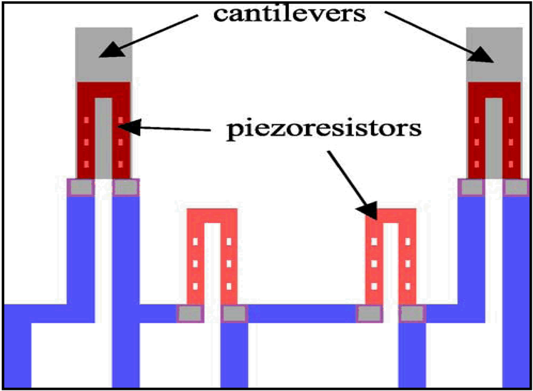
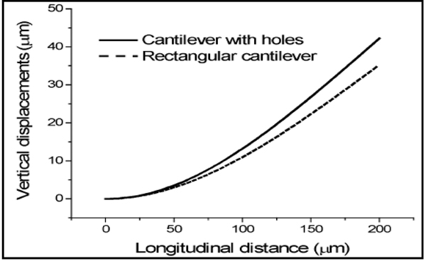
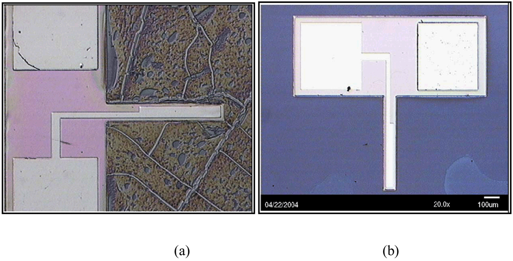
Concentrating the stress to a designated area is another approach to enhance the sensitivity. Yu et al. reported a method to concentrate the stress by introducing holes in the MCLs. These holes cause the stress to be concentrated in its vicinity. The size of the holes is 10 µm × 5 µm [1]. The results showed the MCLs with holes were 1.3 times more sensitive than those without holes in response to the same MCL deflection (Figure 6 and 7). This increase in the surface stress is attributed to the discontinuity of the MCL structure due to the holes.
Figure 6.
The layout of a Wheatstone bridge design of piezoresistive MCLs with stress concentrating holes.
Figure 7.
Stress distribution vs. vertical displacements of MCLs with and without holes.
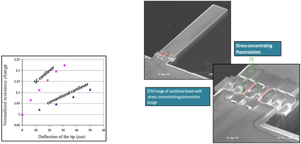
Decreasing the thickness of the cantilevers is a common strategy to increase the sensitivity. However, thin MCLs are more fragile and harder to handle than the thicker ones. Naeli et al. came up with another stress-concentrating design that made it possible to achieve both high sensitivity and toughness. In this design, they separated the stress in the piezoresistors from the stress on the beam structure. In fabrication, the piezoresistive strings were realized on the wafer surface with a cavity underneath. Two thin piezoresistive clamped silicon beams were released on the surface of the cantilever. The new piezoresistive design showed an increase in the relative resistance change by a factor of 5.2 as shown in Figure 8, compared to a cantilever with the same thickness and conventional piezoresistor design. [2].
Figure 8.
Left: Comparison between conventional and stress-concentrating MCLs. Right: SEM images of stress-concentrating beams isolated from MCL base.
2.4 Integration with piezoactuators
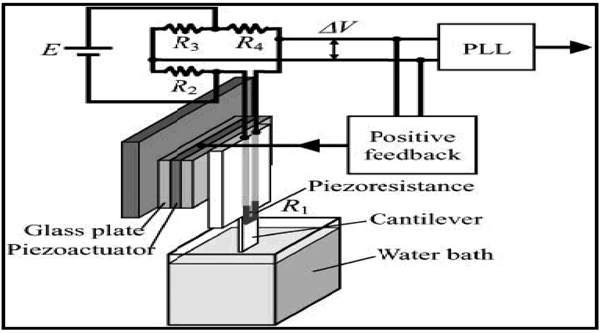
Piezoresistive cantilever can also detect mass change by integration with piezoactuators. Sone et al. introduced a MCL device that consists of a piezoresistive design, a Wheatstone bridge circuit, a positive feedback controller, an exciting piezoactuator, and a phase-locked loop (PLL) demodulator which is shown in Figure 9. In the design, R1 represents the piezoresistive cantilevers in the Wheatstone bridge. The oscillator includes a positive feedback system, a preamplifier, and a piezoactuator driver. The phase locked loop circuit is used for demodulating the frequency signals from the circuit. Results showed that a mass sensitivity of 190 fg/Hz and a mass resolution of about 500 fg were obtained in water. The mass sensitivity is 100 times greater than that of a quartz crystal oscillation system [4].
Figure 9.
A harmonic vibration mass biosensor system based on MCLs [4].
2.5 Minimizing the thermal effect
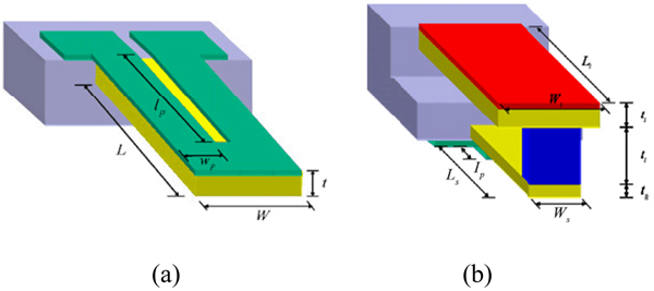
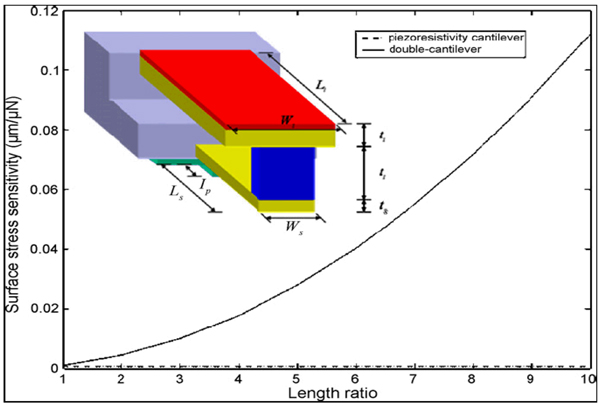
One concern in the field of piezoresistive cantilever sensors is that the sensor performance is readily influenced by the thermal stress during operation. Yang et al. developed a double–MCL design to overcome the thermal stress effect which improves the sensitivity as shown in Figure 10 [5]. The double MCL is composed of a top immobilized MCL and a bottom sensing MCL. These two cantilevers are connected in a way that the biaxial surface stress in the former can be converted to uniaxial strain in the latter. The sensitivity of the double cantilever could be increased by increasing the length ratio or by decreasing the thickness ratio of the two MCLs (Figure 11). More than two orders of sensitivity enhancement have been achieved and the induced thermal effects are minimized.
Figure 10.
(a) Conventional cantilever system with only one cantilever (b) double cantilever design with one cantilever on the top and another at the bottom [5].
3. Capacitive readout scheme
A capacitive readout scheme consists of a microcantilever over an electrode which is ground biased as shown in Figure 12. In a capacitive sensing scheme, an AC voltage of frequency higher than that of the mechanical bandwidth of the cantilever is applied. The output current measured with respect to the applied voltage gives the capacitance value which is a measure of the displacement of the cantilever.
Figure 12.
Basic schematic of a capacitive microcantilever [7]
The capacitive current at the output due to the cantilever displacement is given as [11]:
| (5) |
where ‘C’ is the capacitance between the cantilever beam and the driver.
This capacitance consists of static component Cp and a component c(t) which represents the capacitance because of the displacement of the cantilever.
The first term in the above equation, indicates the parasitic current, and the second term, indicates the current due to the oscillation of the cantilever [11].
The main advantages of capacitive microsensors are low-power high sensitivity, simple structures, low temperature sensitivity and low cost integration of the read out to the portable systems. It outdraws peizoresistive systems because of its low power consumption [27].
3.1 Elimination of the parasitic effect
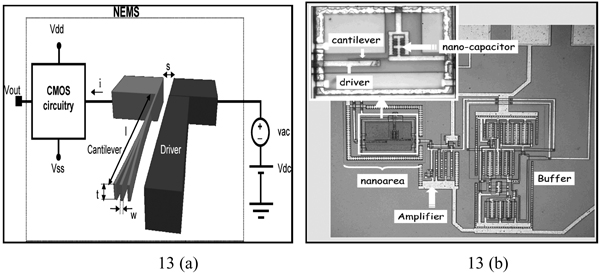
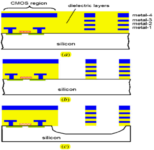
Electrostatic transduction in the nanometer-size regime requires the minimization of the parasitic capacitance [11] to increase the sensitivity. CMOS circuitry for excitation and read-out of the cantilever deflection as shown in Figure 13 has been used to eliminate the parasitic capacitance induced by the external bonding pads and wires [9, 11, 12]. This CMOS circuitry is integrated with the cantilever by using a monolithic technology that consists of the combination of standards CMOS processes and nanofabrication methods. The integrated system demonstrated a high sensitivity and a high spatial resolution (on the order of 10−18 g and 300 nm, respectively) and also introduces less noise compared to resistive and transimpedance methods. Furthermore, by reducing the size of cantilever to nanometer scale, the Q-factor has dramatically increased from 50 to 100 (in air) from 20–30,000 (in vacuum), and reduced the parasitic capacitance to 3 fF [11].
Figure 13.
(a) NEMS system based on a vibrating cantilever monolithically integrated on to a CMOS circuitry. (b) Optical images of the nano-mechanical resonator integrated to a voltage amplifier.
It is shown from the Equation 6, that the sensitivity of the capacitive cantilever sensor improves as the parasitic capacitance is decreased [11].
| (6) |
where Vp − parasitic voltage,Vd − DC voltage, Vg − resulting voltage. This system has shown a reduction in parasitic capacitance to approximately 3fF, which is sufficiently low for the capacitive readout system to function.
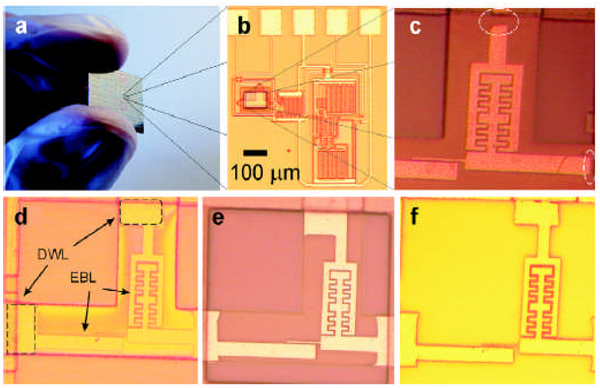
In order to achieve higher sensitivity, S.Ghatnekar-Nilsson et al. researched on fabrication, development of nano-mechanical resonator, and integration systems. The fabrication technique employed here is based on Electron Beam Lithography (EBL), as shown in Figure 14, which is followed by several etching steps. The advantage of driving EBL using low acceleration voltage is that the devices with dimensions less than 50 nm can be easily patterned by this technique, resulting in high sensitivity, low energy consumption, short response times, and minimizing the irradiation damage on CMOS chips [12].
Figure 14.
Optical images of combined EBL and DWL.
The poly-Si thickness is roughly 600nm and underneath SiO2 is 1µm layer. As it was found out that some nano areas have insufficient patterns at the edges when a 3kV electron beam is applied, a newly developed method, Direct Write Laser Lithography (DWL) is applied after the EBL exposure, where the patterns are insufficient. The inherent resonant frequency when a 0V DC is applied is found to be 1.49MHz and when a 7V DC is applied, the resonant frequency was found to be 1.48MHz. This decrease in frequency with an increase in DC voltage was because of the electrostatic spring softening of the system. The increased mass sensitivity of this system is estimated to be 17 Ago Hz−1 [12].
3.2 CMOS cantilevers sensing in femtogram range
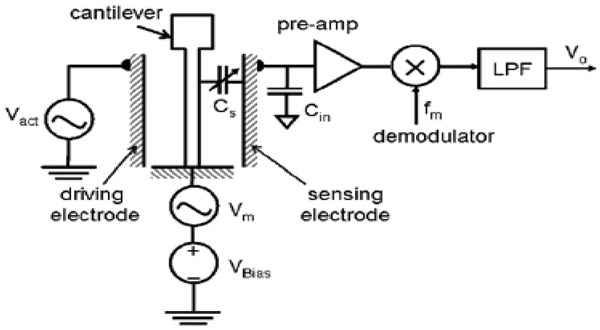
For sensing of the small interaction force between a tip and a surface and small mass loading, resonating cantilevers are used in atomic force microscopy and biochemical sensors. Ying-Chung Li et al. proposed a design, fabrication method, and characterization of the CMOS micromachined cantilevers for mass sensing in femtogram range. Here the cantilever is actuated to resonance by in-plane electrodes, as shown in Figure 16, whose resonant frequency is detected capacitively with on-chip circuitry.
Figure 16.
Circuit diagram of electrostatically driven cantilever to read the resonant frequency shift.
In order to avoid capacitance fed through the driving electrode, single modulation is applied, and this modulated signal is demodulated to the base band and low-pass filtered to remove the undesirable harmonics at high frequencies. The sensitivity is measured by the Equation 7.
| (7) |
where the spring constant is expressed as
| (8) |
The resonant frequencies of these electrostatically driven cantilevers are usually in the order of few hundred kHz for sensitivity enhancement. For a cantilever beam of 3µm wide and 75µm long, the sensitivity is found to be 3.9 fg Hz−1. Further improvement in the sensitivity is done by reducing the cantilever dimensions in order to increase the resonant frequency.
3.3 Techniques to improve sensitivity of humidity sensors
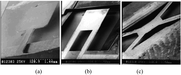
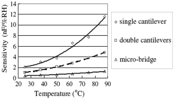
Presence of humidity causes, bending of microcantilever which results in capacitance change between microcantilever and the substrate. Chia-Yen Lee proved that higher sensitivity can be achieved with lower stiffness microcantilever and larger electrode area. In order to increase the sensitivity of the cantilever the beam stiffness should be decreased and the shape of the beam should be optimized. This work shows the sensitivity comparison of three cantilever structures: single, double, and microbridge as shown in Figure 17.
Figure 17.
(a) Single cantilever (b) Double cantilever (c) Micro bridge [8]
The sensors were fabricated by applying a new fabrication approach where the silicon microstructures were suspended above a glass substrate. The humidity sensor cantilever fabricated, has a square shaped beam at the end which also has a temperature sensor in it. The thickness of the beam fabricated is measured to be 20 µm. Then it is spin coated with a polymide layer, which acts as a sensing layer.
The three sensors were tested in a closed chamber with humidity level ranging from 45 % RH to 95 %RH. They compared the study between single, double and micro-bridge cantilever with the same beam dimensions of 2860µm × 400µm × 20µm.
It is seen from Figure 18 that the sensitivity of single cantilever is highest and is directly related to the increase of temperature. The dependence of the sensitivity of single cantilever on the temperature is given by Equation 9.
| (9) |
The results even showed a correlation between the experimental and the simulated results. This sensor has also showed low hysteresis and higher stability.
Figure 18.
Sensitivity Vs temperature for single, double and microbridge cantilevers [8].
3.4 Fabrication techniques to improve sensitivity
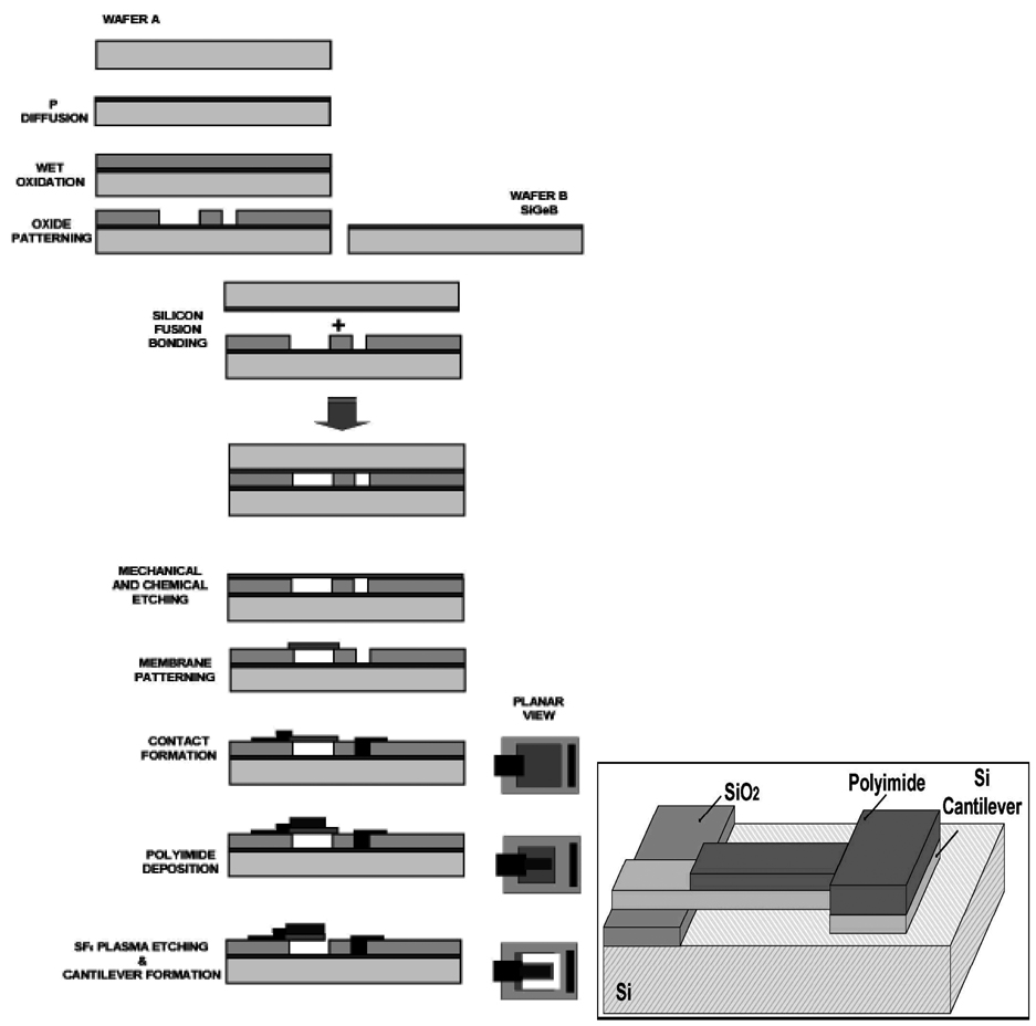
Fabrication of cantilevers plays an important role in increasing the sensitivity of capacitive cantilevers. Chatzandroulis. S et al. developed a fabrication process to enhance the sensitivity of the humidity sensors. For this Si microstructures are suspended at a small distance over the silicon substrate and are released at the final stage by dry etching. This process helps in avoiding stiction of the cantilever with the below laying substrate which is a most evident problem in capacitive cantilever sensors. Figure 19 shows the fabrication steps involved in the fabrication of cantilever sensor.
Figure 19.
(a) Fabrication process for suspended Si microstructures (b) Final cantilever released after dry etching [14].
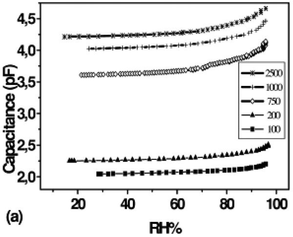
Testing of the above fabricated humidity sensors is done in a closed chamber. From the Figure 20 it is seen that sensitivity increases sharply at higher humidity levels, due to the dielectric constant reaching a value of 6 fF/% RH at 95% RH. Sensitivity as low as 1fF/%RH is achieved through this approach.
Figure 20.
Capacitive response to humidity of five polyimide covered cantilevers [14].
4. Piezoelectric Readout Technique
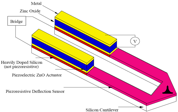
Another recently booming technique to measure the cantilever’s deflection or its resonant frequency is the piezoelectric readout mechanism. The piezoelectric cantilevers consumes power as less as 25% as that of the optical and the piezoresistive sensing element and has sensitivity on par with optical and piezoresistive method [18] making them the most reliable and cost-effective sensors. Piezoelectricity is the property of a material in which a potential is developed across a material when it is subjected to strain; also referred to as direct piezoelectric effect and conversely it undergoes physical strain when a potential is applied to it; commonly referred as indirect piezoelectric effect [16]. Hence a piezoelectric microcantilever can be used for actuation as well as sensing. Piezoelectric force sensor sensitivity is 0.44fC n/m which is three times that of a ZnO force sensor, making its application in scanning force microscope for its higher force sensitivity [26].
There is a choice of wide variety of piezoelectric materials for fabricating microcantilevers. The most commonly used materials for fabricating MCL sensors are ZnO and Lead Zirconium Titanate (LZT) [14–17]. These materials are usually deposited at the fixed ends of MCL as shown in Figure 21. The deposition of the piezoelectric films onto the cantilever is carried out by several methods which include metal organic chemical vapor deposition MOCVD [19], hydrothermal method [20], sputtering [21], pulsed laser deposition [22], and Sol-gel method [23]. Among all these methods sol-gel deposition method is considered to be the most cost effective and convenient method. This is because of the formation of highly homogenous piezoelectric layer and its composition can be readily controlled. The orientation of these layers also plays a pivotal role in determining its sensitivity. A piezoelectric layer with an orientation of <100> is used because its piezoelectric constant is 1.7 times of that of <111> orientation. Higher piezoelectric constant normally results in higher sensitivity [24]. Other than the orientation, the thickness of the film, mechanical, and thermal stress at the film’s interface, the roughness of the surface also plays a major role in determining the piezoelectric constant [25].
Figure 21.
Basic schematic of piezoelectric MCL [14]
The factors that determine the sensitivity of the piezoelectric microcantilever are discussed below.
4.1 Optimized cantilever geometry
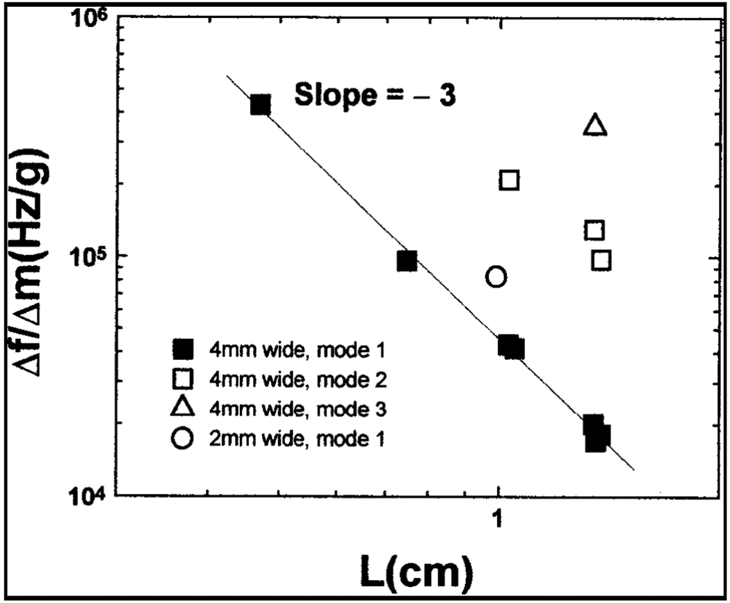
The piezoelectric cantilever dimensions play a crucial role in determining the piezoelectric constant and resonance frequency which in turn determines the sensitivity of the cantilever. Yi et al investigated the effect of piezoelectric cantilever’s length, width and resonance mode on its sensitivity by determining the resonant frequency shift per mass change (Δf/Δm). The tip of the piezoelectric unimorph cantilever (made up of PZT and stainless steel layer) was loaded with point mass. The resulting resonance frequency change was determined and compared experimentally and theoretically.
As we can observe from the Figure. 22, Δf/Δm is larger when the cantilever dimensions are smaller. The influence of the cantilever’s dimensions and the material’s property on the resonance frequency shift, Δf, with respect to the loaded mass, Δm is given by Equation 10 [16]:
| (10) |
As it can be seen Δf/Δm is directly proportional to Eigen value υ2n and inversely proportional to length, ‘L’, and width, ‘w’. Ẽ is the effective Young’s modulus and ρ̃ is the effective density of the unimorph cantilever. So, by keeping the thickness of the cantilever, Young’s modulus and density constant and decreasing the cantilever length and width by a factor of ‘α’, Δf/Δm can be increased by a factor of ‘ α−4’[16].
Figure 22.
Δf/Δm vs. L for all the modes and widths [16]
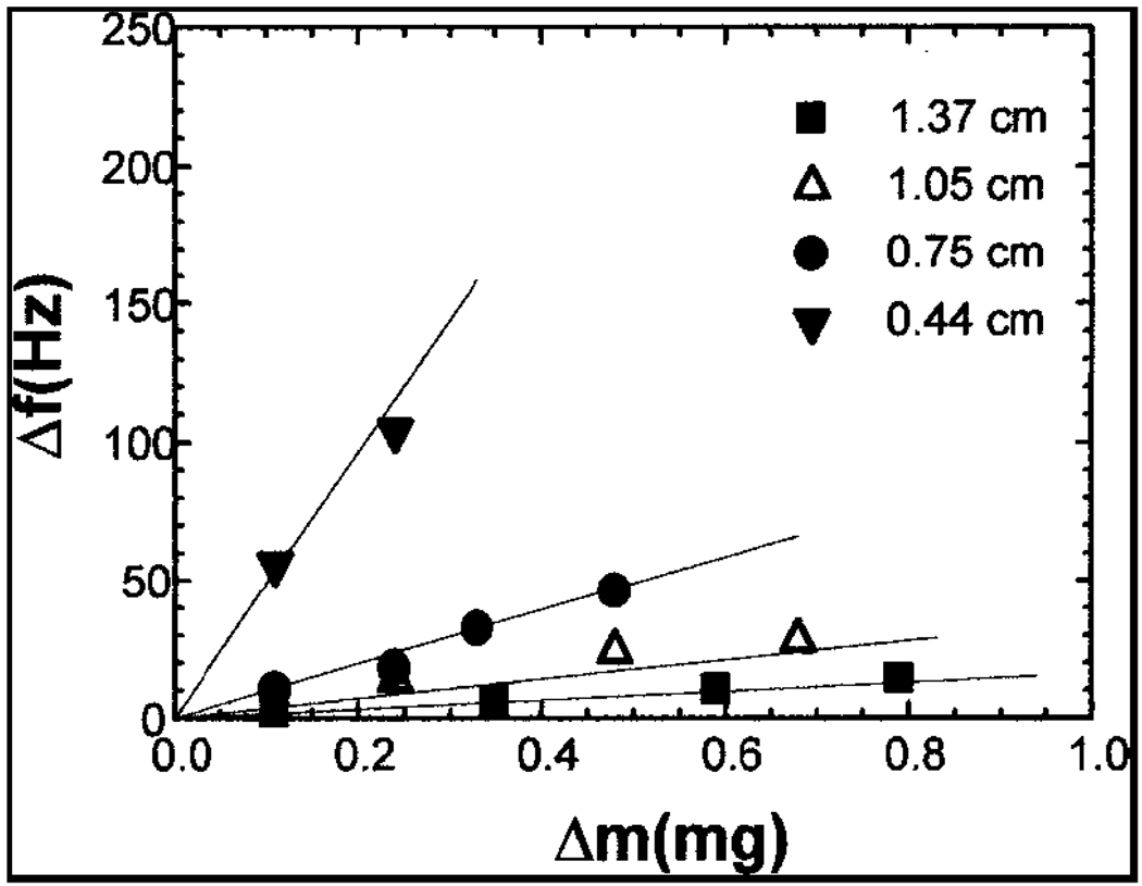
From the Figure 23 it can be seen that for the same width of the MCL the resonance frequency shift increases as the cantilever length increases. This is proved both theoretically (solid lines) and experimentally (symbols) by their closer correlation. Effect of the width on the frequency shift was also analyzed by keeping the length of the cantilever constant (1.05 cm) and by varying the cantilever’s width.
Figure 23.
Experimental and theoretical Δf with respect to Δm of the cantilever with width 0.4cm and varying lengths [16].
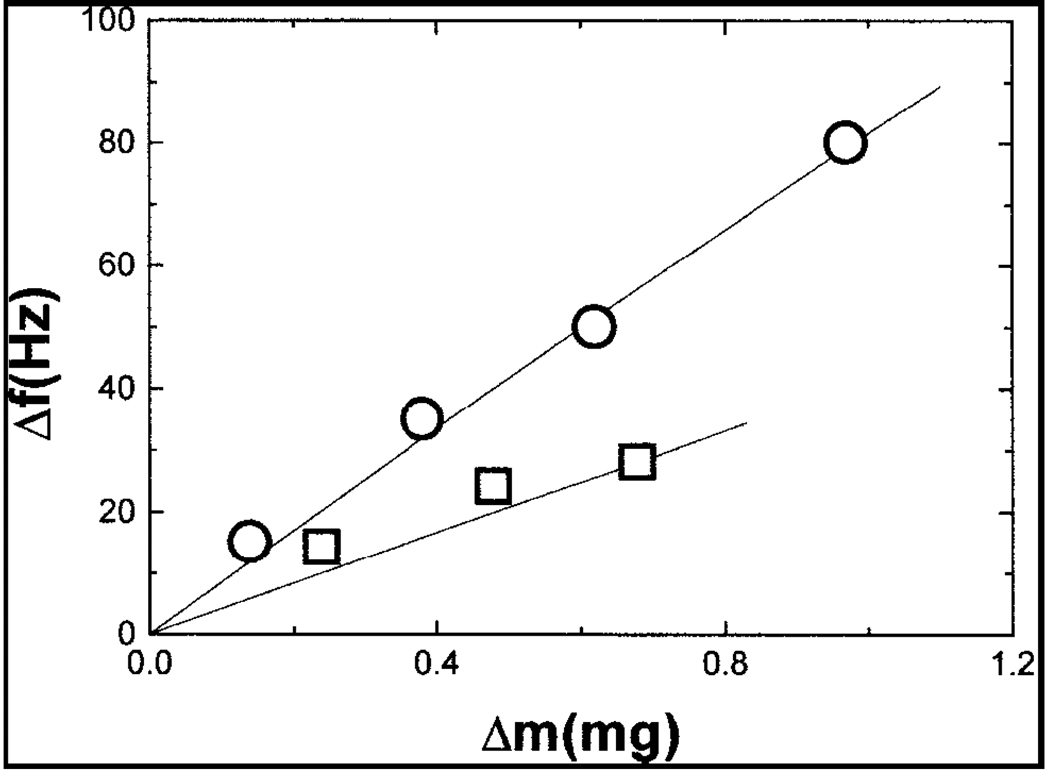
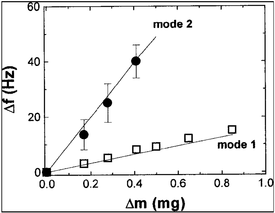
As seen from the Figure 24, the frequency shift is larger when the cantilever dimensions are smaller. This is proved both theoretically (solid lines) and experimentally (symbols). The influence of the resonance mode of the cantilever on its sensitivity was also determined by taking cantilevers of length 1.03cm and width 0.4cm. Figure 25 shows that the frequency shift is larger for a mode 2 operating cantilever than the mode 1 with respect to change in mass. The experimental data (symbols) match well with that of the theoretical data (solid lines). Hence, the functioning of piezoelectric cantilever depends a lot on the dimensions and the mode of working.
Figure 24.
Experimental and theoretical Δf with respect to Δm of the cantilever with length 1.05cm, width 0.4cm (squares) and length 0.99cm, widths 0.2 cm (circles)[16].
Figure 25.
Experimental and theoretical Δf with respect to Δm of the cantilever with length 1.03cm, width 0.4cm in width at mode 1 (squares) and mode 2 (circles)[16].
4.2 Substrate effect on Sensitivity
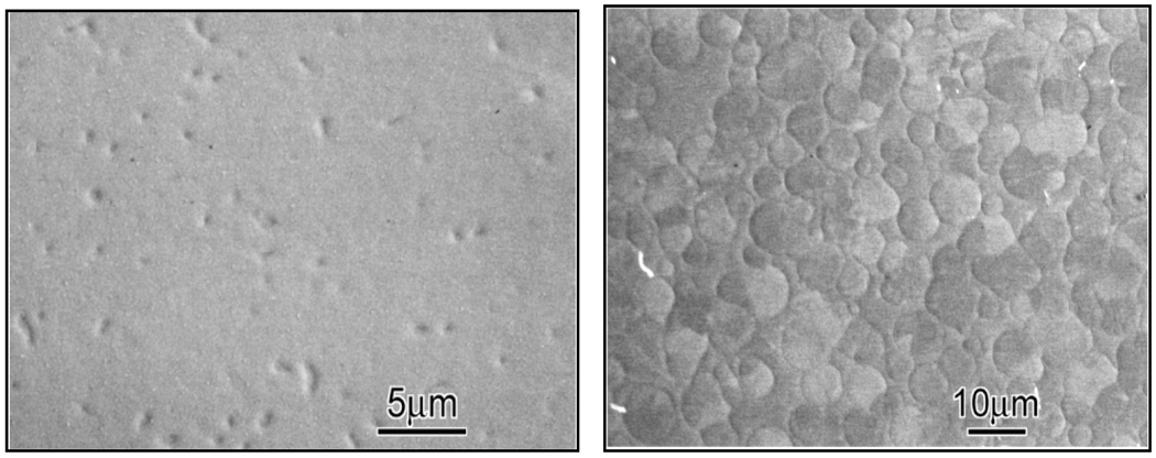
Another factor influencing the sensitivity of the piezoelectric cantilever is the material that is used as the substrate on which piezoelectric layer is deposited. Zhan jie Wang et al. experimented to show the optimum material as a substrate for a piezoelectric MEMS device. Lead zirconate titanate (PZT) thin films were fabricated and coated with Pt/Ti/SiO2 and Ir/IrO2/SiO2/Si substrate. As mentioned earlier, material with <100> orientation tends to have higher piezoelectric constant [17]. Their investigation on the crystalline orientation using the X-ray diffractometer (XRD) showed that PZT film fabricated on Pt/Ti substrate has a highly preferred orientation in the direction of <100> and showed no preferred orientation with Ir/IrO2 substrate. This is because Ir undergoes oxidation during annealing and the PZT layer deposition on the randomly oriented IrO2 layer does not produce <100> orientation. Hence, the PZT deposited on Pt/Ti substrate has a higher piezoelectric constant. By this, they have proved that the substrate plays a major role in the surface morphology which is important for a smooth and uniform surface. As shown in the Figure. 26, PZT layer on Pt/Ti surface was much smoother and uniform than the PZT layer on Ir/IrO2.
Figure 26.
SEM image of PZT layer deposited on (a) Pt/Ti and (b) Ir/IrO2. [17]
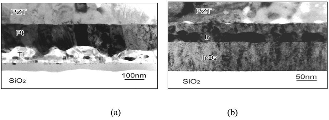
On observation it was found that the PZT film was crystallized with columnar grains in the case of Pt/Ti substrate and without columnar grains in the case of Ir/IrO2. This implies that the substrate influences the nucleation of the PZT films [17] as well. To further investigate this, TEM image of the cross section of PZT/Pt/Ti/SiO2 and PZT/Ir/IrO2/SiO2 was taken as shown in Figure 27.
Figure 27.
TEM image of cross sectional of (a) PZT/Pt/Ti/SiO2 (b) PZT/Ir/IrO2/SiO2 [17]
They have analyzed by the X-ray spectroscopy that the SiO2 region is filled with Pb. This shows that the Pb is diffused into the SiO2 layer. This proves that Pb is not an efficient diffusion barrier. It is observed that Pt/Ti interface is non uniform whereas PZT/Pt interface is smooth and uniform. We can also observe that IrO2 /SiO2 interface is clear and uniform acting as a good barrier to Pb. This is because of the intermediate layer present at the PZT/Ir interface. Hence, we can summarize that Pt/Ti has the preferred orientation but poor barrier effect. IrO2 has a very good barrier effect but poor orientation property. So, Pt/IrO2 is believed to be the suitable substrate for the fabrication of PZT films in order to achieve higher piezoelectric constant and less defective microstructures.
4.3 Improving sensitivity by polling
One more drawback in most of the piezoelectric MCL sensor is that it consists of two separate electrodes, of which one is used for sensing and the other is used for actuation. Weijie Dong et al developed a new PZT piezoelectric MCL device which has two separated electrodes on the top which could be used both for sensing as well as actuation [18]. They showed the influence of the electrode’s length over the sensitivity. They have fabricated an array of three PZT piezoelectric MCLs in which each cantilever consists of an electrode on its surface which in turn is segmented in to two electrodes.
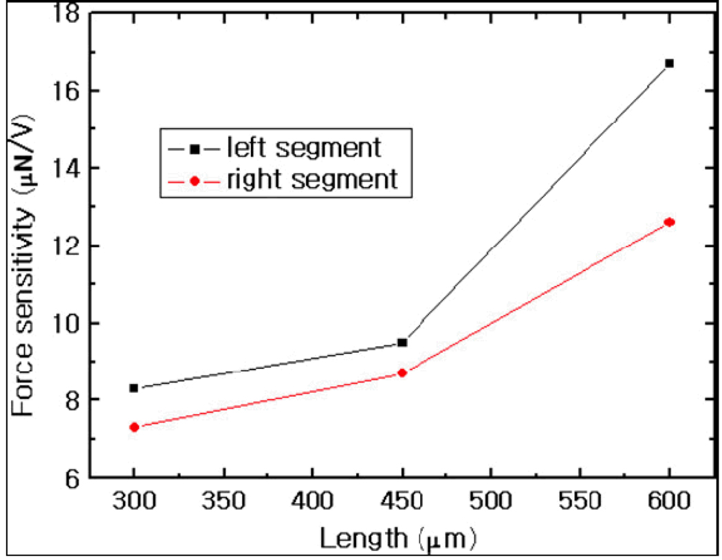
They showed that the length of each segmented electrode plays a major role in determining the sensitivity of the cantilever. As shown in Figure 29, the left segment showed higher sensitivity compared to the right segment since it is longer than the right. They suggested that the length of the left segment should be two times of the right segment for smaller actuation force and higher sensitivity [18].
Figure 29.
Sensitivity for Left and Right segment [18].
They also proposed a new fabrication technique wherein the PZT layer is subjected to poling. The PZT layer is polarized at 100°C with an electric field of 125kV/cm for 1 hour [10]. By this they have increased the sensitivity by two times. Before poling, the cantilever sensibility was 1.61 pC /µm which upon poling rose to 3.25 pC /µm. This increase in the sensitivity is attributed to the increase in the piezoelectric constant of the PZT layer upon poling. Hence poling is proved to be an efficient process for improving the PZTs piezoelectric property and thereby the sensitivity of the MCL.
4.4 Optimized positioning of piezoelectric layer
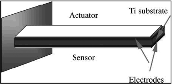
Liqun du et al fabricated a piezoelectric MCL which was applied in touch sensors [19]. Figure 31 shows the sensor unit. The top and bottom layer of the MCL was made of PZT layer which was synthesized by hydrothermal method. These two layers were placed on titanium substrate. The top layer acts as actuation layer and the bottom one acts as sensing layer.
Figure 31.
Schematic of one MCL sensor unit in the touch sensor [19]
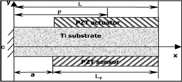
This work showed that the location of the actuation and sensing layer also plays a major role in improving the sensitivity of the cantilever. It was proved that the sensitivity of the cantilever is maximum when the two ends of the actuation and sensing layer were placed at the points where the strain is zero.
In Figure 32, ‘L’ indicates the length of the cantilever, ‘Lp’ represents the length of the sensing and actuation layer, and ‘a’ represents the length between the fixed end of the cantilever and the left edge of the actuation /sensing layer.
Figure 32.
Optimized positioning of the PZT layer for maximum sensitivity [19].
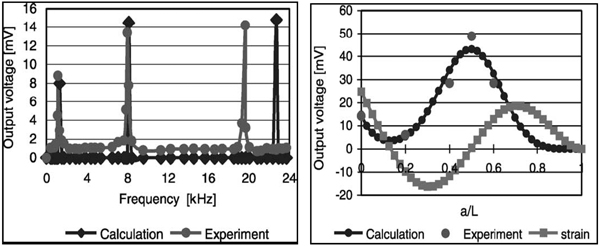
As seen from the Figure 33 (a), the output voltage is large for mode 3. Taking the mode 3 into account it is seen that when the sensing/actuation layers are placed with a/L ratio of 0.5 the output voltage is maximum i.e. the layer is placed such that the free ends are at the points where the strain is zero and the centre lies at the point where the strain is maximum [19].
Figure 33.
(a) Output voltage with respect to frequency, (b) Output voltage with respect to the location of the PZT layer at mode 3 [19].
4.5 Controlling crystallographic orientation
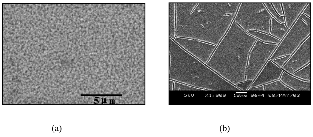
The electrical properties of the piezoelectric material depend majorly on the crystallographic orientation of the piezoelectric material [23]. Some of the traditionally followed methods for improving the crystallographic orientation of PZT (Lead Zirconium Titanate) films are controlled deposition temperature, orientation of Pt substrate and seed layer under the PZT film. The piezoelectric constant of the PZT film increases with the thickness of the PZT layer but may result in cracks after reaching certain limit which is due to the residual stress developed. The cracks formed may decrease the quality of the cantilever and can also result in lower sensitivity. Mengwei liu et al developed a novel method to control the crystallographic orientation of the PZT layer by modifying the process of coating the layers. They tried depositing the PZT layer on the cantilever by five-coating-layer-annealed method and one-coating-layer-annealed method. They observed that as the number of coating layers were increasing voids and hillocks were formed and hence suggested one-layer-coating-annealed sol-gel process for minimizing cracks.
As seen from the Figure. 34, surface undergoing three annealing process has shown lesser cracks compared with the one undergoing four annealing process. This is because the sol-gel process used for fabricating PZT films involves a number of heating treatments which result in crack formation on the layer. Annealing may also result in stress effects on the PZT layer; changing the crystalline structure may also result in the diffusion of PZT into the underlying substrate. All these factors results in undesired functioning of the cantilever sensor and can adversely affect the cantilever’s sensitivity [23].
Figure 34.
(a) SEM image of the surface undergoing three annealing cycles. (b) SEM image of the surface undergoing four annealing cycles [23].
Jin Xie et al. also came up with a novel fabrication idea for overcoming the cracking problem on the PZT layer. In the conventional sol-gel process the PZT films are patterned after the completion of the annealing process. In the proposed process, patterning is done before each post-annealing process. Due to this technique unwanted PZT film is etched out before each annealing step. This can be clearly seen in the Figure 35 where the PZT surfaces fabricated by the conventional method and the modified process are compared.
Figure 35.
(a) Cantilever fabricated with conventional method (b) Modified method [15].
This shows that the modified cantilever fabrication process yields MCL sensors with a high sensitivity by minimizing the cracks.
Conclusion
This study focuses on enhancing the sensitivity of a microcantilever sensor operating on piezoresistive, capacitive, and piezoelectric principles by optimizing its dimensions, choosing proper material, and adopting novel fabrication techniques. It is seen that these factors play a significant role in the cantilever sensitivity. Novel designs and fabrications techniques to increase the piezoresistive cantilever sensitivity have been discussed. It is shown that the sensitivity of the cantilevers working on capacitive effect can be improved by minimizing the parasitic effects by CMOS integration. Fabrication approaches which could make the capacitive cantilever sensor to sense up to femtogram range have also been focused. For the piezoelectric MCL sensors we have shown that the sensitivity depends on the dimensions of the device, the substrate on which they are fabricated. The fabrication approaches such as polling, crystallographic orientation of the films, one-coating-annealing-sol-gel-process, and patterning of the device after each annealing process and proper positioning of the piezoelectric material. These factors are taken into consideration in order to increase the piezoelectric constants of the MCLs and avoiding cracking problems as these affects the sensitivity to a greater extent.
Figure 5.
Schematic of a piezoresistive SiO2 MCL.
Figure 11.
Surface stress sensitivity of double and single cantilever systems with respect to the length ratio [5].
Figure 15.
Cross sectional view of CMOS at different steps a) after completion b) anisotropic reactive ion etch c) isotropic silicon etch.
Figure 28.
PZT MCL with right, bottom, and left electrode pads [18].
Figure 30.
Sensing capability of the cantilever before and after polling [18].
Acknowledgement
Dr. Ji would like to thank National Institutes of Health (NIH) Grant Number 1R01NS057366. The contents of this paper are solely the responsibility of the authors and do not necessarily represent the official views of the agencies funding this work.
References
- 1.Yu Xiaomei, Tang Yaquan, Zhang Haitao, Li Ting, Wang Wei. Design of High-Sensitivity Cantilever and Its Monolithic Integration with CMOS Circuits. IEEE Sensors Journal. 2007 April;Vol.7(No. 4):489–495. [Google Scholar]
- 2.Naeli Kianoush, Brand Oliver. Cantilever Sensor with Stress-Concentrating Piezoresistor Design. IEEE. 2006:592–595. [Google Scholar]
- 3.Li Peng, Li Xinxin. A single-sided micromachined piezoresistive SiO2 cantilever sensor for ultra-sensitive detection of gaseous Chemicals. Journal of micromechanical and microengineering. 2006:2539–2546. [Google Scholar]
- 4.Sone Hayato, Ikeuchi Ayumi, Izumi Takashi, Okano Haruki, Hosaka Sumio. Femtogram Mass Biosensor Using Self-Sensing Cantilever for Allergy Check. Japanese Journal of Applied Physics. 2006;Vol. 45(No. 3B):2301–2304. [Google Scholar]
- 5.Yang SM, Yin TI, Chang C. Development of a double-MCL for surface stress measurement in microsensors. Sensors and Actuators B. 2007;121:545–551. [Google Scholar]
- 6.Chivukula Venkata, Wang Ming, Ji Hai-Feng, Khaliq Abdul, Fang Ji, Varahramyan Kody. Simulation of SiO2-based piezoresistive MCLs. Sensors and Actuators A. 2006;125:526–533. [Google Scholar]
- 7.Lavrik NV, Sepaniak MJ, Datskos PG. Cantilever transducers as a platform for chemical and biological sensors. Review of scientific instruments. 2004 July;Vol. 75(No.7):2229–2253. [Google Scholar]
- 8.Lee Chia-Yen, Lee Gwo-Bin. Micromachine based humidity sensors with integrated temperature sensors for signal drift compensation. Journal of micromechanics and microengineering. 2003;(No.13):620–627. [Google Scholar]
- 9.Teva J, Abadal G, Torres F, Verd J, Pe´rez-Murano F, Barniol N. A femtogram resolution mass sensor platform, based on SOI electrostatically driven resonant cantilever. Part I: Electromechanical model and parameter extraction. Ultramicroscopy. 2006;(No.106):800–807. doi: 10.1016/j.ultramic.2005.12.016. [DOI] [PubMed] [Google Scholar]
- 10.Chung Eunhyea, Lavrik Nickolay, Datskos Panos, Mcfarlane Joanna, Dai Sheng, Tsouris Costas. Microcantilever sensors with chemically selective coatings of ionic liquids. AIChE Journal. 2007 October;Vol. 53(No. 10):2726–2731. [Google Scholar]
- 11.Verd Jaume, Abadal G, Teva J, Gaudó María Villarroya, Uranga Arantxa, Borrisé Xavier, Campabadal Francesca, Esteve Jaume, Costa Eduardo Figueras, Pérez-Murano Francesc, Davis ZacharyJ, Forsén Esko, Boisen Anja, Barniol Nuria. Design, fabrication, and characterization of a submicroelectromechanical resonator with monolithically integrated CMOS readout circuit. Journal of microelectromechanical systems. 2005 June;vol. 14(No. 3):508–519. [Google Scholar]
- 12.Ghatnekar-Nilsson1 S, Forsén E, Abadal G, Verd J, Campabadal F, P´erez-Murano F, Esteve J, Barniol N, Boisen A, Montelius L. Resonators with integrated CMOS circuitry for mass sensing applications, fabricated by electron beam lithography. Institute of physics publishing, Nanotechnology. 2005;(No.16):98–102. [Google Scholar]
- 13.Li YC, Ho MH, Hung SJ, Chen MH, Lu MSC. CMOS Micromachined Capacitive Cantilevers for Mass Sensing. Journal of Micromechanics and Microengineering. 2006;Vol. 16:2659–2665. [Google Scholar]
- 14.Chatzandroulis S, Tserepi A, Goutouridis D, Normand P, Tsoukalas D. Fabrication of Single Crystal Si Cantilevers Using a Dry Release Process and Application in a Capacitive-Type Humidity Sensor. Microelectronic Engineering. 2002;Vol. 61:955–961. [Google Scholar]
- 15.Xie Jin, Hub Min, Ling Shih-Fu, Dua Hejun. Fabrication and characterization of piezoelectric cantilever for micro transducers. Sensors and Actuators. 2006;A-126:182–186. [Google Scholar]
- 16.Yi JeongWoo, Shih WanY, Shih Wei-Heng. Effect of length, width, and mode on the mass detection sensitivity of piezoelectric unimorph cantilevers. Journal of applied physics. 2002 February;volume 91(no.31):1680–1686. [Google Scholar]
- 17.Wang ZhanJie, Chu JiaRu, Maeda Ryotaro, Kokawa Hiroyuki. Effect of bottom electrodes on microstructures and electrical properties of sol–gel derived Pb(Zr0.53 Ti0.47)O3 thin films. Thin Solid Films. 2002;416:66–71. [Google Scholar]
- 18.Dong Weijie, Lu Xiaoguang, Liu Mengwei, Cui Yan, Wang Jing. Measurement on the actuating and sensing capability of a PZT MCL. Meas. Sci. Technol. 2007:601–608. [Google Scholar]
- 19.Shimizu M, Okaniwa M, Fujisawa H, Niu H. Ferroelectric properties of Pb(Zr, Ti)O3 thin films prepared by low-temperature MOCVD using PbTiO3 seeds. J. Eur.Ceram. Soc. 2004;24:1625–1628. [Google Scholar]
- 20.Liqun D, Guiryong K, Fumihito A, Toshio F, Kouichi I, Yasunori T. Structure design of micro touch sensor array. Sensors Actuators, A-107. 2003;A-107:7–13. [Google Scholar]
- 21.Thomas R, Mochizuki S, Mihara T, Ishida T. Effect of substrate temperature on the crystallization of Pb(Zr, Ti)O3 films on Pt/Ti/Si substrates prepared by radio frequency magnetron sputtering with a stoichiometric oxide target. Mater. Sci. Eng. 2002;B-95:36–42. [Google Scholar]
- 22.Husmann A, Wesner DA, Schmidt J, Klotzbücher T, Mergens M, Kreutz EW. Pulsed laser deposition of crystalline PZT thin films. Surf. Coat. Technol. 1997;97:420–425. [Google Scholar]
- 23.Liu Mengwei, Wang Jing, Wang Liding, Cui Tianhong. Deposition and characterization of Pb(Zr, Ti)O3 sol-gel thin films for piezoelectric cantilever beams. Smart Mater. Struct. 2007;No.16:93–99. [Google Scholar]
- 24.Gong W, Li J, Zhu X, Gui Z, Li L. Preparation and characterization of sol–gel derived (100)-textured Pb (Zr, Ti) O3 thin films: PbO seeding role in the formation of preferential orientation. Acta Mater. 2004;52:2787–2793. [Google Scholar]
- 25.Udayakumar KR, Schuele PJ, Chen J, Krupanidhi SB, Cross LE. Thickness-dependent electrical characteristics of lead zirconate titanate thin films. J. Appl. Phys. 1995;77:3981–3986. [Google Scholar]
- 26.Lee C, Itoh T, Sasaki G, Suga T. Sol-gel derived PZT force sensor for scanning force microscopy. Materials Chemistry and Physics. 1996;No.44:25–29. [Google Scholar]
- 27.Tortonese M, Yamada H, Barrett RC, Quate CF. Atomic force microscopy using piezoresistive cantilever. Solid state sensors and actuators, IEEE. 1991:448–451. [Google Scholar]


