Abstract
We demonstrate the synthesis of monolayer graphene using thermal chemical vapor deposition and successive transfer onto arbitrary substrates toward transparent flexible conductive film application. We used electron-beam-deposited Ni thin film as a synthetic catalyst and introduced a gas mixture consisting of methane and hydrogen. To optimize the synthesis condition, we investigated the effects of synthetic temperature and cooling rate in the ranges of 850–1,000°C and 2–8°C/min, respectively. It was found that a cooling rate of 4°C/min after 1,000°C synthesis is the most effective condition for monolayer graphene production. We also successfully transferred as-synthesized graphene films to arbitrary substrates such as silicon-dioxide-coated wafers, glass, and polyethylene terephthalate sheets to develop transparent, flexible, and conductive film application.
Keywords: Graphene, Chemical vapor deposition, Transfer, Raman spectroscopy, Transparent, Flexible, Conductive film
Introduction
Graphene is a newly discovered carbon-based monolayer sheet consisting of honeycomb structures with two-dimensional arrays [1]. It has been attracting great attention owing to its fascinating mechanical, electronic, and optical properties [1-3]. Fundamental and application research is being carried out intensively in order to determine the potential uses. Several approaches to synthesizing graphene have been developed, including mechanical and chemical exfoliation, thermal chemical vapor deposition (TCVD), the graphitization of silicon carbide, and the reduction of graphene oxides [4-8].
The TCVD method is considered an appropriate method for the large area synthesis of graphene [5,9]. However, there is still a definite need for high-quality graphene production that also yields large area thickness uniformity. In addition, the synthesis mechanism remains poorly understood and requires further study [9,10]. In terms of the industrial application aspects, its outstanding electrical conductivity in a plane and high elasticity makes graphene a powerful candidate material not only for various functional devices such as sensors and electronic elements but also for transparent flexible conductive (TFC) electrodes that can replace indium tin oxide film and therefore be used in flexible display, touch screens and flexible solar cells via transfer onto flexible and transparent receiving substrates [11]. In this context, a large area synthesis with high thickness uniformity and successful transfer ability are essential and urgent topics in the realization of the aforementioned applications.
Here, we demonstrate the optimization of monolayer graphene synthesis using TCVD and the subsequent transfer onto arbitrary substrates toward TFC film application. We mainly investigated the effects of synthetic temperature and cooling rate on graphene thickness. We found that synthesis at 1,000°C and a cooling rate of 4°C/min was the most effective combination for monolayer graphene production. We also successfully transferred as-synthesized graphene films onto arbitrary substrates such as silicon-dioxide-covered wafers, glass, and polyethylene terephthalate (PET) polymer sheets for further development as TFC films.
Experimental Details
As a graphene synthesis substrate, Ni thin films (300 nm thickness) were deposited by electron-beam evaporation using a SiO2-covered Si wafer. The substrate was cut to 2 cm × 2 cm in size and installed in a 1-inch quartz tube furnace, as shown in Fig. 1. The tube was evacuated using a mechanical pump and then filled with Ar gas until atmospheric pressure was reached. While heating to the synthesis temperature range of 850–1,000°C, a mixture of H2 (500 sccm) and Ar (500 sccm) gas was used under ambient pressure. The heating rate was 20°C/min. After the synthesis temperature was reached, we held it 30-min further to stabilize the furnace and to obtain a single-crystalline Ni phase, as suggested in a previous report [12]. The gas was then promptly changed into a mixture consisting of CH4 (5 sccm) and H2 (1,500 sccm) that was flowed during the 10-min synthesis. The effect of cooling rate on the graphene microstructure was investigated by modulating the cooling rate to 2, 4, 6, and 8°C/min through intentional cooling using a fan.
Figure 1.
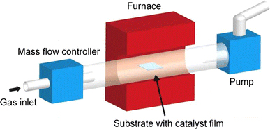
Schematic illustration of a graphene synthesis system
Synthesized samples on a Ni catalytic layer were first examined using an optical microscope and an atomic force microscope (AFM, Park Systems XE-70). A representative optical microscopic image of as-grown samples at 1,000°C with a 4°C/min cooling rate is shown in Fig. 2a. We can distinguish the grain boundary of the Ni film and can also estimate the quality of graphene samples qualitatively since the thinner graphene region is light gray while the thicker regions are dark gray. In the AFM topographic image of the same sample (Fig. 2b), it was found that the grain boundary of the Ni film can be resolved and the partially folded region of the formed graphene sheet can be shown as linear lines with 3 nm height.
Figure 2.
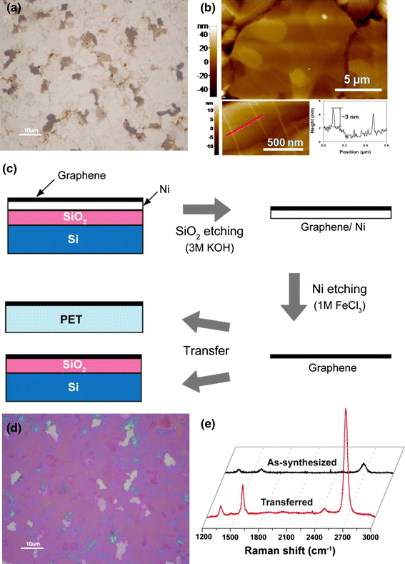
a Optical microscope image and b AFM topographic image of as-synthesized graphene on Ni catalytic films. Lower insets of (b) show graphene wrinkles on the substrate with 3 nm height. c Schematic presentation showing the graphene transfer without a polymeric mediator. d Optical microscope image of transferred graphene on a SiO2-covered Si wafer. e Raman spectra show the intensity enhancement after the transfer
After synthesis, we performed graphene transfer to a SiO2-covered Si wafer, glass plates, and PET sheets for further development. Here, we tried to carry out the transfer without a polymeric mediator such as polymethyl methacrylate film to prevent potential contamination during the removal of the polymeric films and thus preserve the clean surface of the as-synthesized graphene, as schematically shown in Fig. 2c. In brief, we first etched silicon dioxide using a 3M KOH solution at 75°C and obtained a catalytic Ni layer covered with graphene. The temperature of the solution was sensitive to removal of the SiO2 layer. Then, we further etched out the Ni layer using a 1M FeCl3 solution. When the Ni layer was completely removed, the graphene began floating on the solution and was discernable with the naked eye; we were thus able to scoop it up using receiving substrates. For optical microscopic observation, we used SiO2 (300-nm thick)-coated Si wafers since we can clearly determine the number of graphene layers by color differences (Fig. 2d).
We were able to obtain enhanced Raman profiles after the transfer compared to the pristine samples on Ni films, as shown in Fig. 2e. Raman spectroscopy is a useful and convenient tool to examine the structural property of graphenes [13,14]. Here, we used a 532-nm excitation wavelength laser with 1 μm spot size and low power of less 3 mW (Horiba Aramis). The Raman spectra ranges of 1,000–3,000 cm−1 from as-synthesized and transferred samples are comparatively shown in Fig. 2e. We obtained intensive peaks around 1,350, 1,600, and 2,700 cm−1, which are known as the defect-induced D-band, the graphitic C–C vibration-related G-band, and the G′-band, which is an overtone of the D-band, respectively. In mono layer graphene, the G′-band shows a single Lorentzian profile below Raman frequency of 2,700 cm−1 and the intensity ratio of the G-band and the G′-band (IG/IG′) is below unity. As the number of graphene layers increases, the value of IG/IG′ decreases over unity and the line shape also becomes asymmetric.
Transmission electron microscopy (TEM, JEM2100 F) was used to reveal the detailed nanostructures of as-synthesized graphenes. The graphene samples for observation were prepared by direct transfer onto a TEM copper grid. For the characterization of the graphene-transferred-TFC film, the sheet resistance was measured by the four-point probe method, and transparency measurement was performed using incident light of 550-nm wavelength.
Results and Discussion
We first investigated the effect of synthesis temperature on the thickness uniformity of graphene; the results are shown in Fig. 3. The growth temperatures were 1,000, 900, and 850°C; the optical images taken after transfer onto the SiO2 wafer are given in Fig. 3a–3c, respectively. As shown in Fig. 2d, we can easily distinguish monolayer graphene from the magenta color of the optical image, as indicated by the square in Fig. 3a. As the thickness of graphene increases, the color changes to purple as shown in Fig. 3b. The thickest area, which has more than 15 graphene layers, looks white, as shown in Fig. 3a. The estimation of graphene layers using optical images showed good concurrence with the results of Raman characterization, as shown in Fig. 3d. It was thus very useful to estimate the areal uniformity of the graphene samples with different growth parameters. The sample processed at 850°C had no graphene over the substrate (Fig. 3c); this was also reconfirmed by the Raman analysis (Fig. 3d). On the basis of this result, it can be concluded that the synthetic temperature to produce graphene is a minimum of 900°C. It was found in the Raman spectra that the value of IG/IG′ decreases from 1.6 (>15 layers) to 0.86 (>7 layers) and 0.4 (monolayer) with the decrease in graphene layers. It is interesting to note that very thick graphene regions (>15 layers) are locally observed only in the 1,000°C samples although the areal coverage of monolayer graphene in the 1,000°C sample is higher than that of the 900°C sample. It is expected that the enhanced surface diffusion of carbon on Ni films in a 1,000°C environment gives rise to a locally distributed very thick graphene region among the relatively large monolayer area when we take account of the graphene synthesis mechanism which is composed of feedstock dissolution, supersaturation, and precipitation of carbon on Ni catalysts [15]. In other words, insufficient carbon diffusion at 900°C results in relatively low areal monolayer coverage with moderate thickness as shown in Fig. 3b. We thus fixed the synthesis temperature at 1,000°C hereafter.
Figure 3.
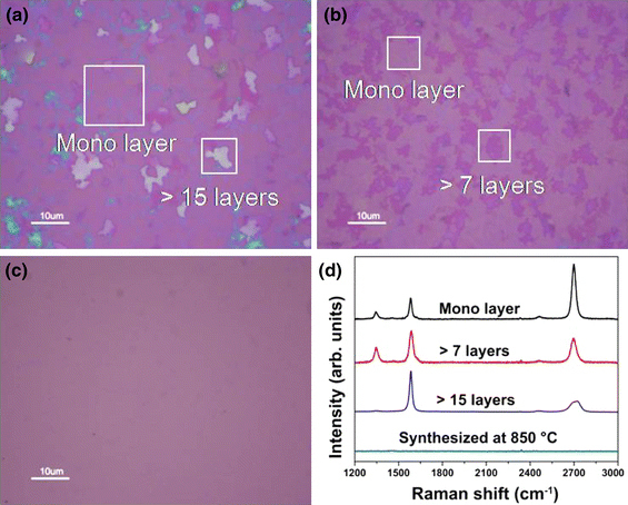
Optical microscope images of synthesized graphenes at different temperatures: a 1,000°C, b 900°C, and c 850°C. d Raman spectra depend on the number of graphene layers in the samples
Next, we investigated the effect of cooling rate on the thickness uniformity of graphene since we expected that the carbon precipitation and diffusion on the Ni surface are critical to determining the number of graphene layers and large area synthesis. We fixed the synthesis temperature (1,000°C) and gas composition (CH4:H2 = 5 sccm:1,500 sccm) so that we could ensure the same condition in the amount of carbon influx and decomposed carbon species. The cooling rate after the 1,000°C synthesis was changed to 8, 6, 4, and 2°C/min; their optical images are shown in Fig. 4a–4d, respectively.
Figure 4.
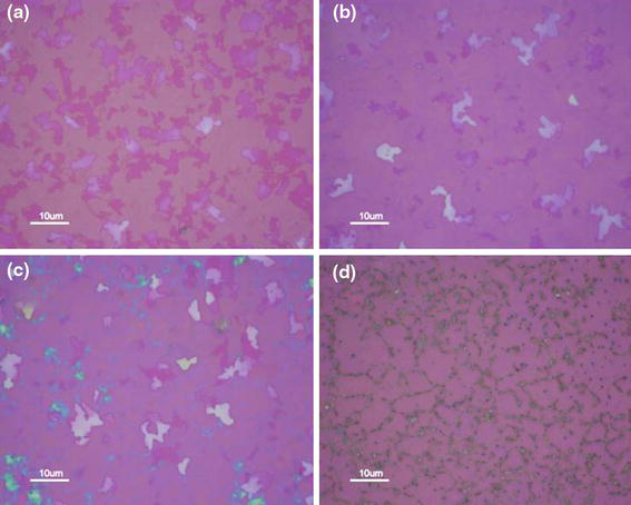
Optical microscope images of synthesized graphenes with different cooling rates: a 8°C/min, b 6°C/min, c 4°C/min, and d 2°C/min
The optical image of the fastest cooled sample has very similar features as the 900°C-grown sample, which means that the carbon diffusion is insufficient, as shown in Fig. 4a. On the other hand, we can observe a mixture of monolayer and thick layer graphenes in the 6°C/min sample (Fig. 4b). The portion of thick graphene layer increased with decreasing cooling rate to 4°C/min (Fig. 4c), which implies that the enhanced surface diffusion of carbon might be responsible for the increased number of thick graphene spots through the Ostwald ripening phenomena in particle agglomeration. However, with a very low cooling rate of 2°C/min, it seemed that the precipitated carbon was sufficiently diffused and finally made some carbonaceous compound along the grain boundary, as shown in Fig. 4d.
The aforementioned optical observation results were confirmed with the Raman results obtained from the representative area of each sample (Fig. 5a). We confirmed that the main products in the 8°C/min cooled sample are several layered graphenes and that monolayer graphene is formed in the 6 and 4°C/min cooling conditions. For the 2°C/min furnace-cooled sample, we did not observe graphite-related peaks.
Figure 5.
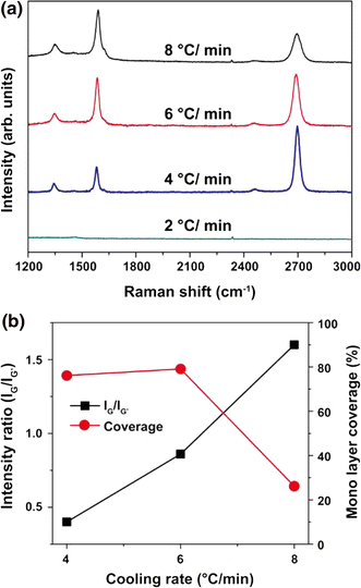
a Raman spectra of synthesized graphenes with different cooling rates. b Effects of cooling rates on both peak intensity ratio (IG/IG′) and areal coverage of monolayer graphenes
We estimated the monolayer coverage based on the color difference of the optical images of Fig. 4. We also determined the value of the intensity ratio (IG/IG′) from the Raman spectra (Fig. 5b). In brief, the areal coverage of graphene monolayer exceeds 75% in 6 and 4°C/min cooling samples while the 8°C/min cooled sample has approximately 26% areal coverage. In the Raman spectra analysis, the value of IG/IG′ reaches 0.4, 0.8, and 1.6 with the increasing cooling rate of 4, 6, and 8°C/min, respectively. We can thus conclude from the results that the optimum temperature and cooling rate of our synthesis system is 1,000°C and 4°C/min, respectively. Figure 6 presents a representative highly magnified TEM image and electron diffraction pattern from the optimized sample. The bright field image shows a folded edge of monolayer graphene. The electron diffraction pattern shows hexagonally distributed several diffraction spots on polycrystalline ring, which means that the pattern is taken from few layered graphenes.
Figure 6.
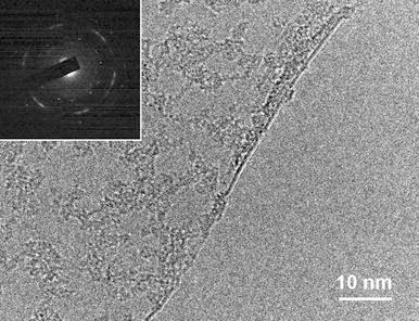
a A representative TEM image of mono layer graphene synthesized at 1,000°C with a 4°C/min cooling rate. The inset shows the electron diffraction pattern of the sample
Finally, we fabricated transparent conductive film using the transfer technique of as-grown graphene in order to apply TFC films; the results are shown in Fig. 7. A transparency of 87% and sheet resistance of 1,540 Ω/sq. were obtained from the 4°C/min cooling sample presented as the left side inset in Fig. 7. The right inset is a digital camera image that shows the good conductivity of the transparent conducting graphene film. The transparency decreased to 73% and the sheet resistance also decreased to 890 Ω/sq. in the 8°C/min cooled sample. The reason for the decrease in the transparency and sheet resistance and the increase in the conductivity is the increased number of graphene layers with the increasing cooling rate. The transparency and conductivity are progressively being enhanced through further development of the system.
Figure 7.
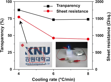
Effects of cooling rates on sheet resistance and optical transmittance at the 550-nm wavelength of graphene-based TFC films. The inset shows a digital camera image of transferred graphene (left) and a demonstration of the illuminator (right)
Conclusions
We demonstrated a growth optimization procedure for monolayer graphene using TCVD and its subsequent transfer onto various substrates toward TFC film application. We investigated the effects of synthetic temperature and cooling rate on graphene structures and found that synthesis at 1,000°C and a cooling rate of 4°C/min were the most effective conditions for monolayer graphene production. We also fabricated graphene-based TFC films via the transfer of as-grown graphene films onto PET or glass substrates without the use of polymeric mediators.
Acknowledgments
This research was supported by Basic Science Research Program (No.2009-0089315) and Converging Research Center Program (No.2009-0083380) through the National Foundation of Korea (NRF) funded by the Ministry of Education, Science and Technology.
Open Access
This article is distributed under the terms of the Creative Commons Attribution Noncommercial License which permits any noncommercial use, distribution, and reproduction in any medium, provided the original author(s) and source are credited.
References
- Zhang Y, Tan Y, Stormer H, Kim P. Nature. 2005. p. 201. COI number [1:CAS:528:DC%2BD2MXhtF2nsrnJ]; Bibcode number [2005Natur.438..201Z] [DOI] [PubMed]
- Novoselov KS, Geim AK, Morozov SV, Jiang D, Katsnelson MI, Grigorieva IV, Dubonos SV, Firsov AA. Nature. 2005. p. 197. COI number [1:CAS:528:DC%2BD2MXhtF2nsrnI]; Bibcode number [2005Natur.438..197N] [DOI] [PubMed]
- Geim AK, Novoselov KS. Nat. 2007. p. 183. COI number [1:CAS:528:DC%2BD2sXit1Khtrg%3D]; Bibcode number [2007NatMa...6..183G] [DOI] [PubMed]
- Novoselov KS, Geim AK, Morozov SV, Jiang D, Zhang Y, Dubonos SV, Grigorieva IV, Firsov AA. Science. 2004. p. 666. COI number [1:CAS:528:DC%2BD2cXos1Kqt70%3D]; Bibcode number [2004Sci...306..666N] [DOI] [PubMed]
- Reina A, Jia X, Ho J, Son H, Bulovic V, Dresselhaus MS, Kong J. Nano Lett. 2009. p. 30. COI number [1:CAS:528:DC%2BD1cXhsVCmurbM]; Bibcode number [2009NanoL...9...30R] [DOI] [PubMed]
- Obraztsov AN, Obraztsova EA, Tyurnina AV, Zolotukhin AA. Carbon. 2007. p. 2017. COI number [1:CAS:528:DC%2BD2sXovFeitL4%3D] [DOI]
- Berger C, Song Z, Li X, Wu X, Brown N, Naud C, Mayou D, Li T, Hass J, Marchenkov AN, Conrad EH, First PN, de Heer WA. Science. 2006. p. 1191. COI number [1:CAS:528:DC%2BD28XkvVOiurk%3D]; Bibcode number [2006Sci...312.1191B] [DOI] [PubMed]
- Dikin DA, Stankovich S, Zimney EJ, Piner RD, Dommett GHB, Evmenenko G, Nguyen ST, Ruoff RS. Nature. 2007. p. 457. COI number [1:CAS:528:DC%2BD2sXotFajurc%3D]; Bibcode number [2007Natur.448..457D] [DOI] [PubMed]
- Li X, Cai W, An JH, Kim SY, Nah JH, Yang D, Piner R, Velamakanni A, Jung IH, Tutuc E, Banerjee SK, Colombo L, Ruoff RS. Science. 2009. p. 1312. COI number [1:CAS:528:DC%2BD1MXms12gtbY%3D]; Bibcode number [2009Sci...324.1312L] [DOI] [PubMed]
- Chae SJ, Günes F, Kim KK, Kim ES, Han GH, Kim SM, Shin HJ, Yoon SM, Choi JY, Park MH, Yang CW, Pribat D, Lee YH. Adv. 2009. p. 2328. COI number [1:CAS:528:DC%2BD1MXnt12ntLw%3D] [DOI]
- Bae S, Kim H, Lee Y, Xu X, Park J, Zheng Y, Balakrishnan J, Lei T, Kim H, Song Y, Kim Y, Kim K, Ozyilmaz B, Ahn J, Hong B, Iijima S. Nat. Published online: 20 June 2010. [DOI]
- Thompson CV. Annu. Rev. Mater. Sci. 1990. p. 245. COI number [1:CAS:528:DyaK3MXnt1Chug%3D%3D]; Bibcode number [1990AnRMS..20..245T] [DOI]
- Ferrari AC, Meyer JC, Scardaci V, Casiraghi C, Lazzeri M, Mauri F, Piscanec S, Jiang D, Novoselov KS, Roth S, Geim AK. Phys. 2006. p. 187401. COI number [1:STN:280:DC%2BD28jitlersg%3D%3D]; Bibcode number [2006PhRvL..97r7401F] [DOI] [PubMed]
- Gupta A, Chen G, Joshi P, Tadigadapa S, Eklund PC. Nano Lett. 2006. p. 2667. COI number [1:CAS:528:DC%2BD28Xht1Sjur3K]; Bibcode number [2006NanoL...6.2667G] [DOI] [PubMed]
- Yu Q, Lian J, Siriponglert S, Li H, Chen YP, Pei SS. Appl. Phys. Lett. 2008. p. 113103. Bibcode number [2008ApPhL..93k3103Y] [DOI]


